Downloaded 107 times


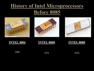
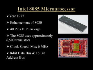
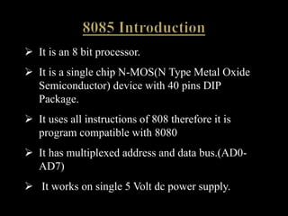
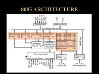


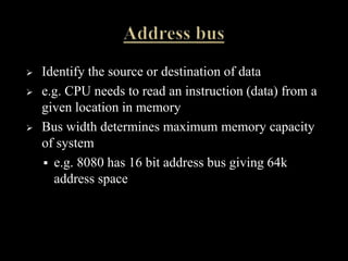
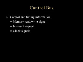

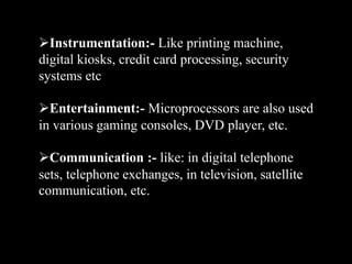

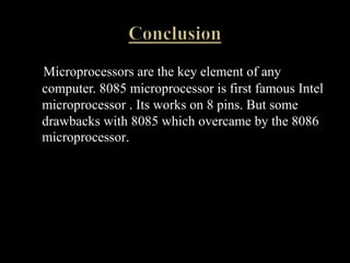


The document discusses the Intel 8085 microprocessor. It provides details on the architecture and pin diagram of the 8085. The 8085 is an 8-bit processor introduced in 1977 as an enhancement of the 8080. It has a maximum clock speed of 6MHz and can access 64KB of memory using its 16-bit address bus. The document outlines the various components of the 8085 architecture and describes its applications in areas like printing, gaming, and communications. It notes some disadvantages of the 8085 like potential overheating and limited data size.