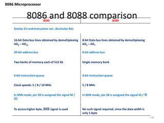
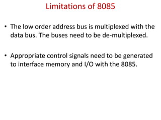
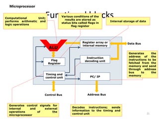
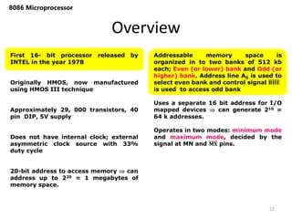
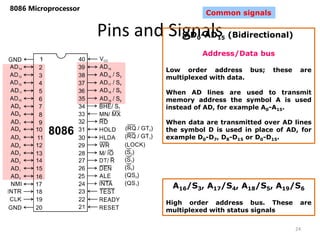
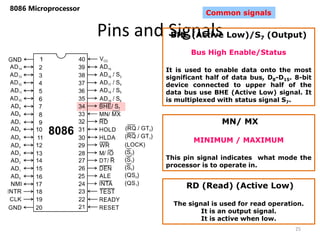
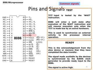
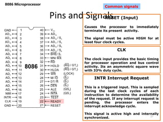
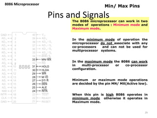
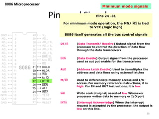
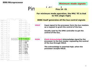
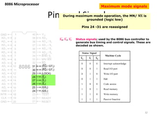
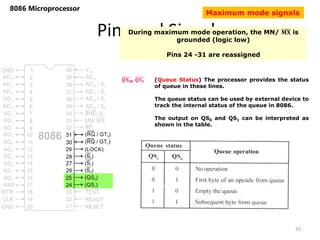
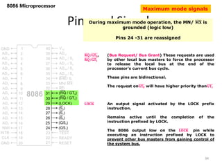
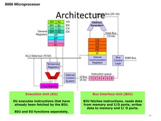
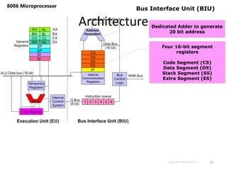
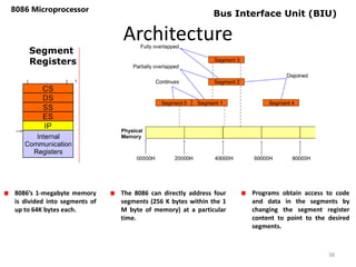
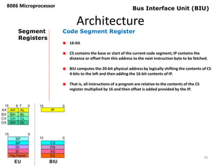
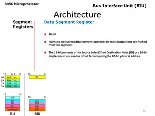
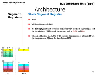
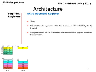
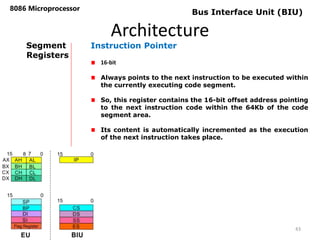
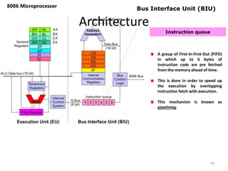
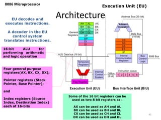
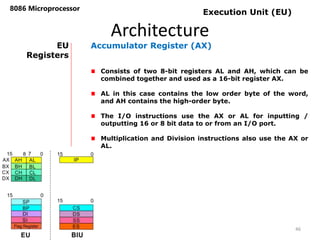
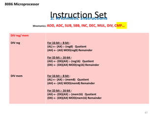
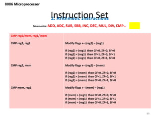
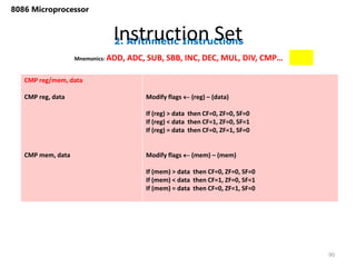
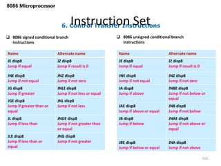
The document describes the architecture and pin configuration of the 8086 microprocessor. It discusses the 8086's 20-bit address bus that can access up to 1 MB of memory. It details the pin functions in minimum and maximum mode, including the address, data, control signals, and status pins. It explains the 8086's internal architecture which includes the bus interface unit and execution unit, as well as its use of segment registers to access different segments of memory.


![Architecture
8086 Microprocessor
48
EU
Registers
Counter Register (CX)
Consists of two 8-bit registers CL and CH, which can be
combined together and used as a 16-bit register CX.
When combined, CL register contains the low order byte of
the word, and CH contains the high-order byte.
Instructions such as SHIFT, ROTATE and LOOP use the
contents of CX as a counter.
Execution Unit (EU)
Example:
The instruction LOOP START automatically decrements
CX by 1 without affecting flags and will check if [CX] =
0.
If it is zero, 8086 executes the next instruction;
otherwise the 8086 branches to the label START.](https://image.slidesharecdn.com/applicationof8086and8085microprocessorinrobots-240229070731-199b2217/85/Application-of-8086-and-8085-Microprocessor-in-Robots-pptx-48-320.jpg)

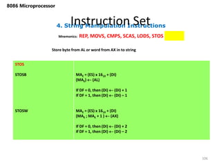
![Addressing Modes
66
8086 Microprocessor
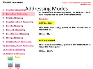
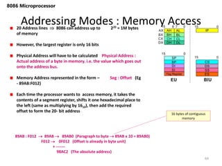
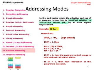
1. Register Addressing
2. Immediate Addressing
3. Direct Addressing
4. Register Indirect Addressing
5. Based Addressing
6. Indexed Addressing
7. Based Index Addressing
8. String Addressing
9. Direct I/O port Addressing
10. Indirect I/O port Addressing
11. Relative Addressing
12. Implied Addressing
Here, the effective address of the memory
location at which the data operand is stored is
given in the instruction.
The effective address is just a 16-bit number
written directly in the instruction.
Example:
MOV BX, [1354H]
MOV BL, [0400H]
The square brackets around the 1354H denotes
the contents of the memory location. When
executed, this instruction will copy the contents of
the memory location into BX register.
This addressing mode is called direct because the
displacement of the operand from the segment
base is specified directly in the instruction.
Group II : Addressing modes for memory
data](https://image.slidesharecdn.com/applicationof8086and8085microprocessorinrobots-240229070731-199b2217/85/Application-of-8086-and-8085-Microprocessor-in-Robots-pptx-63-320.jpg)
![Addressing Modes
67
8086 Microprocessor
1. Register Addressing
2. Immediate Addressing
3. Direct Addressing
4. Register Indirect Addressing
5. Based Addressing
6. Indexed Addressing
7. Based Index Addressing
8. String Addressing
9. Direct I/O port Addressing
10. Indirect I/O port Addressing
11. Relative Addressing
12. Implied Addressing
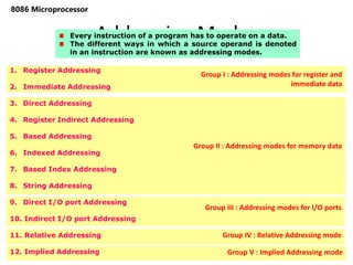
In Register indirect addressing, name of the
register which holds the effective address (EA)
will be specified in the instruction.
Registers used to hold EA are any of the following
registers:
BX, BP, DI and SI.
Content of the DS register is used for base
address calculation.
Example:
MOV CX, [BX]
Operations:
EA = (BX)
BA = (DS) x 1610
MA = BA + EA
(CX) (MA) or,
(CL) (MA)
(CH) (MA +1)
Group II : Addressing modes for memory
data
Note : Register/ memory
enclosed in brackets refer to
content of register/ memory](https://image.slidesharecdn.com/applicationof8086and8085microprocessorinrobots-240229070731-199b2217/85/Application-of-8086-and-8085-Microprocessor-in-Robots-pptx-64-320.jpg)
![Addressing Modes
68
8086 Microprocessor
1. Register Addressing
2. Immediate Addressing
3. Direct Addressing
4. Register Indirect Addressing
5. Based Addressing
6. Indexed Addressing
7. Based Index Addressing
8. String Addressing
9. Direct I/O port Addressing
10. Indirect I/O port Addressing
11. Relative Addressing
12. Implied Addressing
In Based Addressing, BX or BP is used to hold the
base value for effective address and a signed 8-bit
or unsigned 16-bit displacement will be specified
in the instruction.
In case of 8-bit displacement, it is sign extended
to 16-bit before adding to the base value.
When BX holds the base value of EA, 20-bit
physical address is calculated from BX and DS.
When BP holds the base value of EA, BP and SS is
used.
Example:
MOV AX, [BX + 08H]
Operations:
0008H 08H (Sign extended)
EA = (BX) + 0008H
BA = (DS) x 1610
MA = BA + EA
(AX) (MA) or,
(AL) (MA)
(AH) (MA + 1)
Group II : Addressing modes for memory
data](https://image.slidesharecdn.com/applicationof8086and8085microprocessorinrobots-240229070731-199b2217/85/Application-of-8086-and-8085-Microprocessor-in-Robots-pptx-65-320.jpg)
![Addressing Modes
69
8086 Microprocessor
1. Register Addressing
2. Immediate Addressing
3. Direct Addressing
4. Register Indirect Addressing
5. Based Addressing
6. Indexed Addressing
7. Based Index Addressing
8. String Addressing
9. Direct I/O port Addressing
10. Indirect I/O port Addressing
11. Relative Addressing
12. Implied Addressing
SI or DI register is used to hold an index value for
memory data and a signed 8-bit or unsigned 16-
bit displacement will be specified in the
instruction.
Displacement is added to the index value in SI or
DI register to obtain the EA.
In case of 8-bit displacement, it is sign extended
to 16-bit before adding to the base value.
Example:
MOV CX, [SI + 0A2H]
Operations:
FFA2H A2H (Sign extended)
EA = (SI) + FFA2H
BA = (DS) x 1610
MA = BA + EA
(CX) (MA) or,
(CL) (MA)
(CH) (MA + 1)
Group II : Addressing modes for memory
data](https://image.slidesharecdn.com/applicationof8086and8085microprocessorinrobots-240229070731-199b2217/85/Application-of-8086-and-8085-Microprocessor-in-Robots-pptx-66-320.jpg)
![Addressing Modes
70
8086 Microprocessor
1. Register Addressing
2. Immediate Addressing
3. Direct Addressing
4. Register Indirect Addressing
5. Based Addressing
6. Indexed Addressing
7. Based Index Addressing
8. String Addressing
9. Direct I/O port Addressing
10. Indirect I/O port Addressing
11. Relative Addressing
12. Implied Addressing
In Based Index Addressing, the effective address
is computed from the sum of a base register (BX
or BP), an index register (SI or DI) and a
displacement.
Example:
MOV DX, [BX + SI + 0AH]
Operations:
000AH 0AH (Sign extended)
EA = (BX) + (SI) + 000AH
BA = (DS) x 1610
MA = BA + EA
(DX) (MA) or,
(DL) (MA)
(DH) (MA + 1)
Group II : Addressing modes for memory
data](https://image.slidesharecdn.com/applicationof8086and8085microprocessorinrobots-240229070731-199b2217/85/Application-of-8086-and-8085-Microprocessor-in-Robots-pptx-67-320.jpg)
![Addressing Modes
8086 Microprocessor
1. Register Addressing
2. Immediate Addressing
3. Direct Addressing
4. Register Indirect Addressing
5. Based Addressing
6. Indexed Addressing
7. Based Index Addressing
8. String Addressing
9. Direct I/O port Addressing
10. Indirect I/O port Addressing
11. Relative Addressing
12. Implied Addressing
These addressing modes are used to access data
from standard I/O mapped devices or ports.
In direct port addressing mode, an 8-bit port
address is directly specified in the instruction.
Example: IN AL, [09H]
Operations: PORTaddr = 09H
(AL) (PORT)
Content of port with address 09H is
moved to AL register
In indirect port addressing mode, the instruction
will specify the name of the register which holds
the port address. In 8086, the 16-bit port address
is stored in the DX register.
Example: OUT [DX], AX
Operations: PORTaddr = (DX)
(PORT) (AX)
Content of AX is moved to port
whose address is specified by DX
register. 72
Group III : Addressing modes for I/O
ports](https://image.slidesharecdn.com/applicationof8086and8085microprocessorinrobots-240229070731-199b2217/85/Application-of-8086-and-8085-Microprocessor-in-Robots-pptx-69-320.jpg)
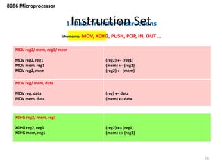
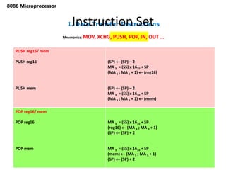
![1. Data Transfer Instructions
Instruction Set
80
8086 Microprocessor
Mnemonics: MOV, XCHG, PUSH, POP, IN, OUT …
IN A, [DX]
IN AL, [DX]
IN AX, [DX]
PORTaddr = (DX)
(AL) (PORT)
PORTaddr = (DX)
(AX) (PORT)
IN A, addr8
IN AL, addr8
IN AX, addr8
(AL) (addr8)
(AX) (addr8)
OUT [DX], A
OUT [DX], AL
OUT [DX], AX
PORTaddr = (DX)
(PORT) (AL)
PORTaddr = (DX)
(PORT) (AX)
OUT addr8, A
OUT addr8, AL
OUT addr8, AX
(addr8) (AL)
(addr8) (AX)](https://image.slidesharecdn.com/applicationof8086and8085microprocessorinrobots-240229070731-199b2217/85/Application-of-8086-and-8085-Microprocessor-in-Robots-pptx-77-320.jpg)


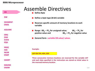
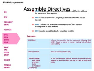
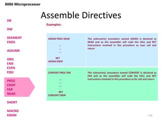
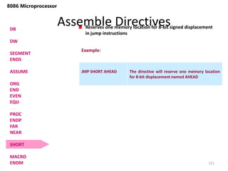
![Assemble Directives
119
8086 Microprocessor
DB
DW
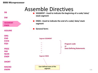
SEGMENT
ENDS
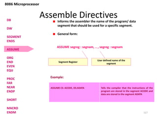
ASSUME
ORG
END
EVEN
EQU
PROC
ENDP
FAR
NEAR
SHORT
MACRO
ENDM
PROC Indicates the beginning of a procedure
ENDP End of procedure
FAR Intersegment call
NEAR Intrasegment call
General form
procname PROC[NEAR/ FAR]
…
…
…
RET
procname ENDP
Program statements of the procedure
Last statement of the procedure
User defined name of the
procedure](https://image.slidesharecdn.com/applicationof8086and8085microprocessorinrobots-240229070731-199b2217/85/Application-of-8086-and-8085-Microprocessor-in-Robots-pptx-116-320.jpg)
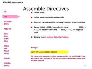
![Assemble Directives
122
8086 Microprocessor
DB
DW
SEGMENT
ENDS
ASSUME
ORG
END
EVEN
EQU
PROC
ENDP
FAR
NEAR
SHORT
MACRO
ENDM
MACRO Indicate the beginning of a macro
ENDM End of a macro
General form:
macroname MACRO[Arg1, Arg2 ...]
…
…
…
macroname ENDM
Program statements
in the macro
User defined name of the macro](https://image.slidesharecdn.com/applicationof8086and8085microprocessorinrobots-240229070731-199b2217/85/Application-of-8086-and-8085-Microprocessor-in-Robots-pptx-119-320.jpg)