Download as PDF, PPTX
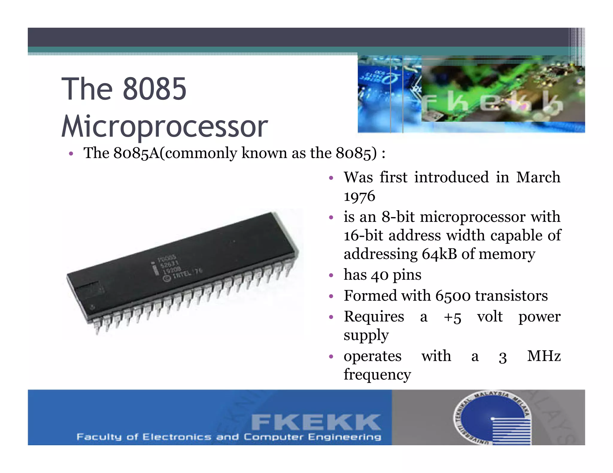

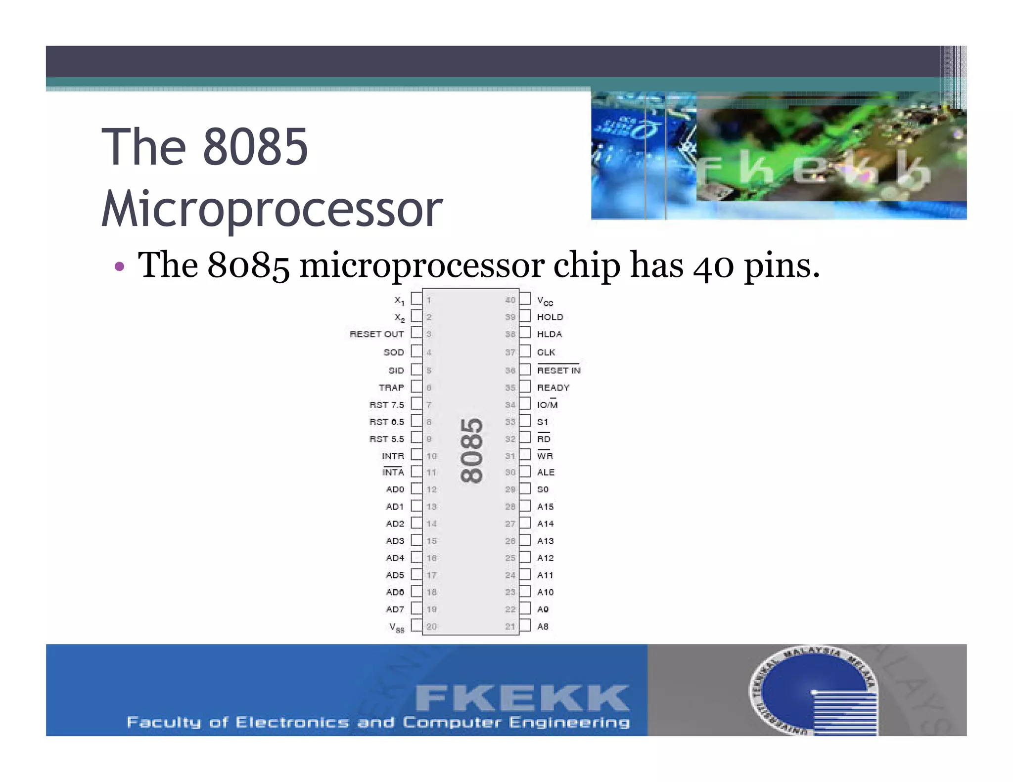


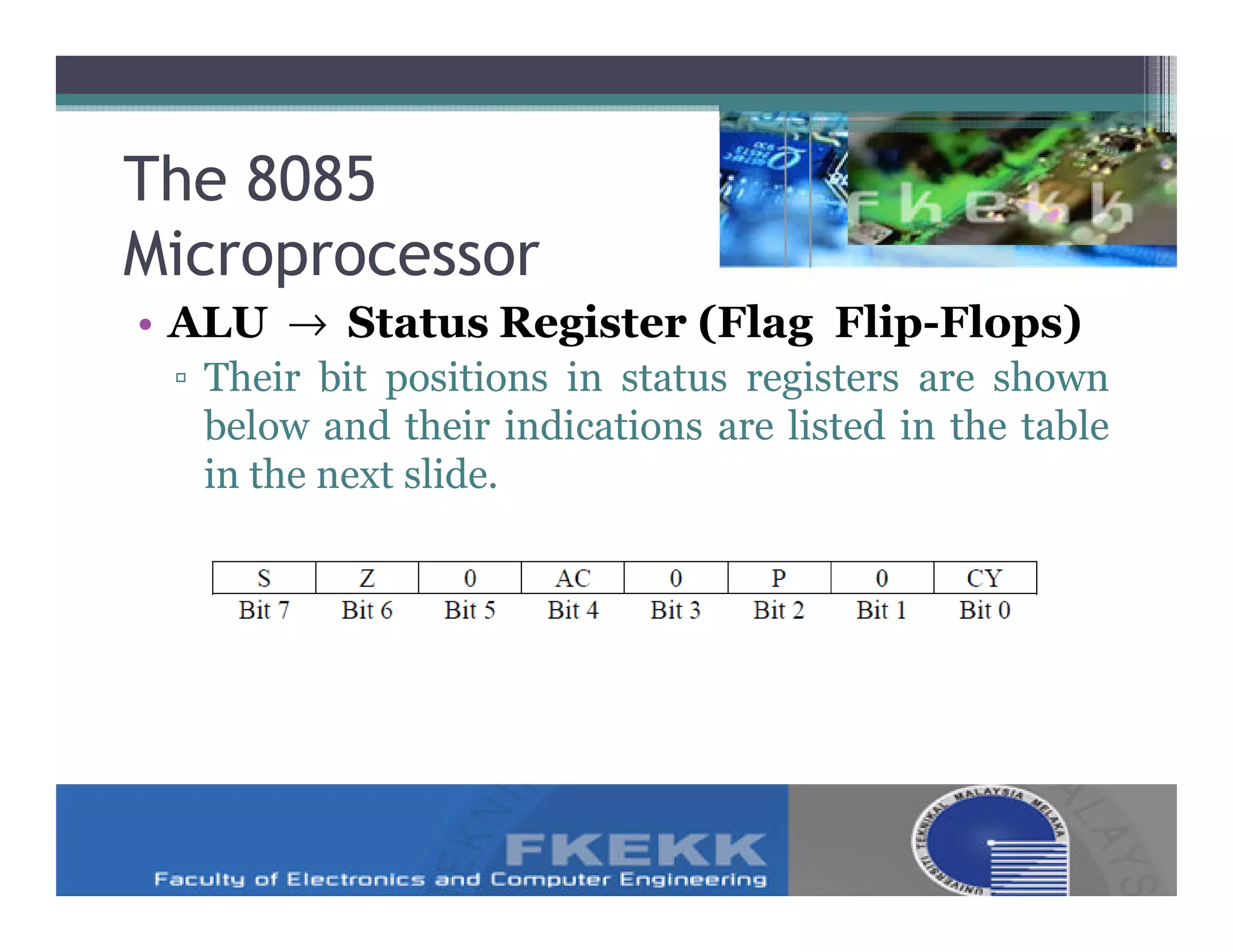
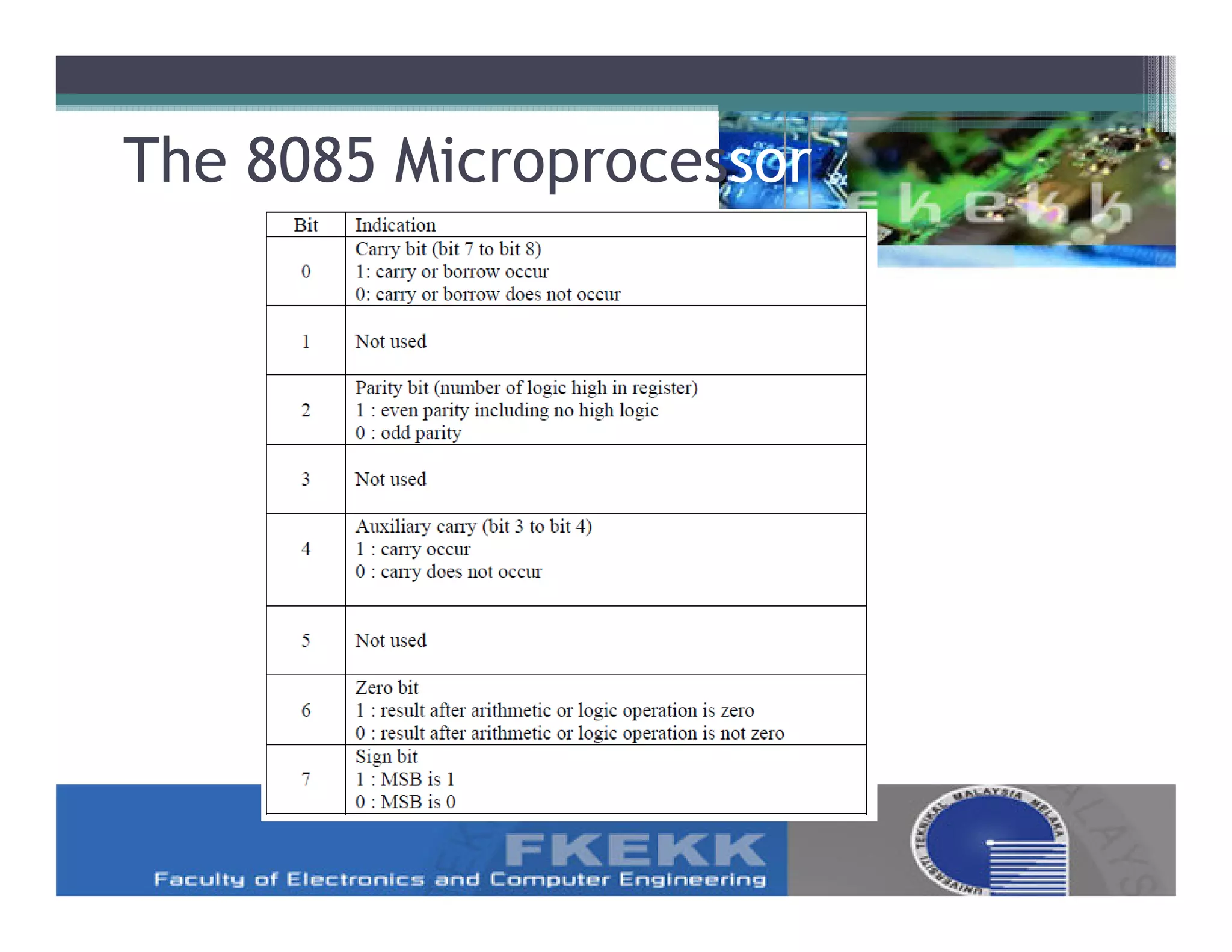


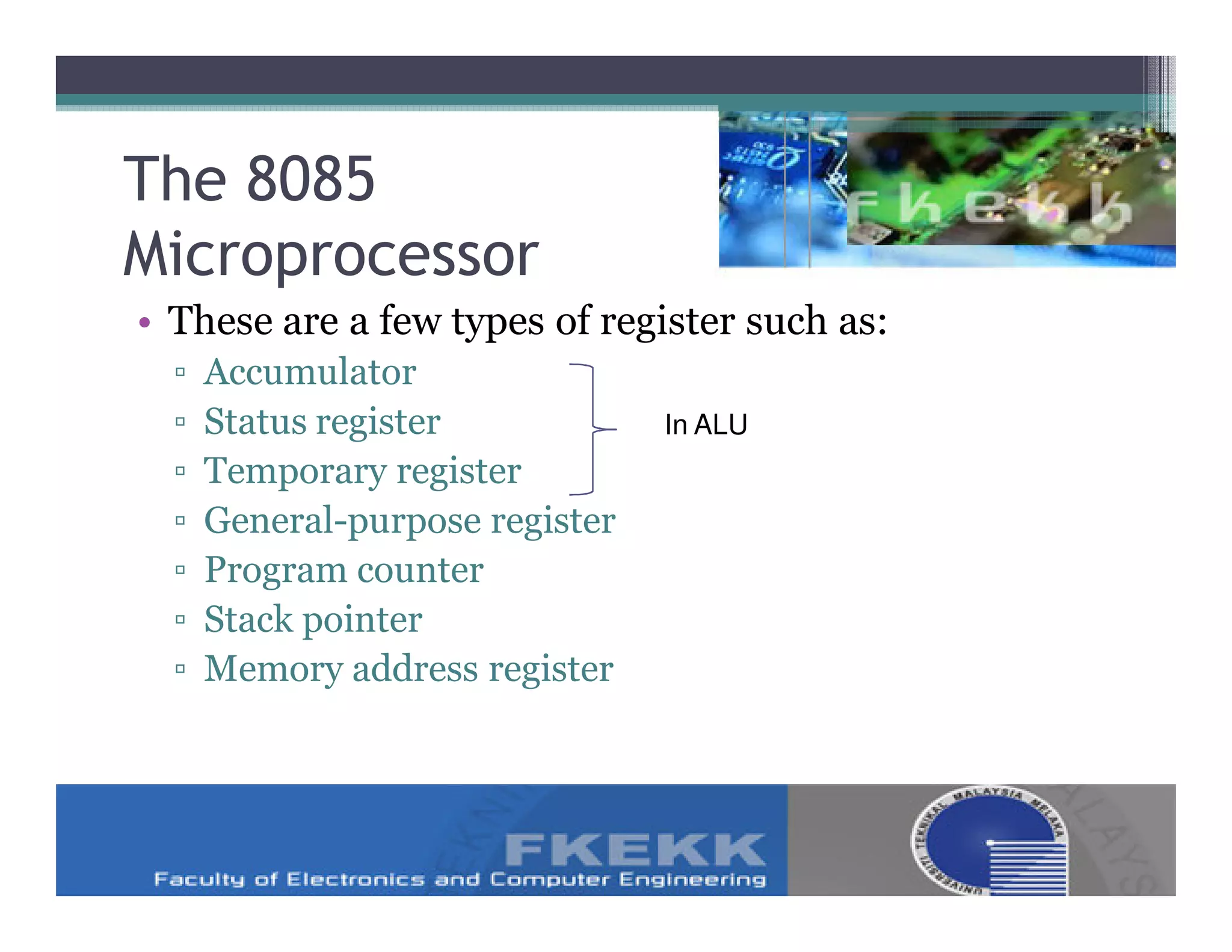


The 8085 microprocessor has 40 pins that are grouped into address bus, data bus, control and status bus, power supply and frequency pins, externally initiated and acknowledgement signals, and serial I/O ports. It was introduced in 1976 and has an 8-bit processor architecture with a 16-bit address bus, allowing it to access up to 64KB of memory. Internally, the 8085 includes an ALU, registers, timing and control unit, instruction register and decoder, and interrupt control unit.