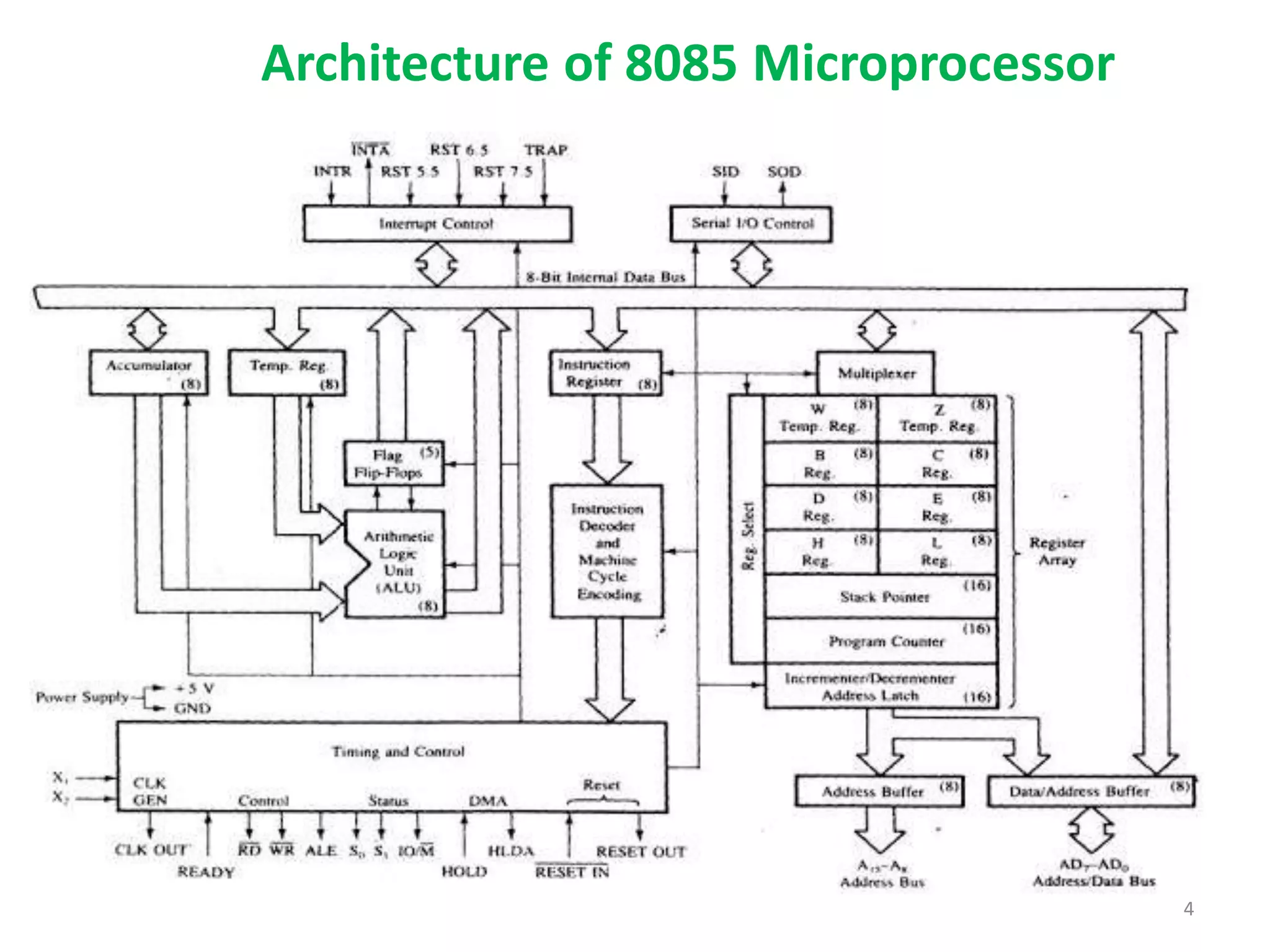
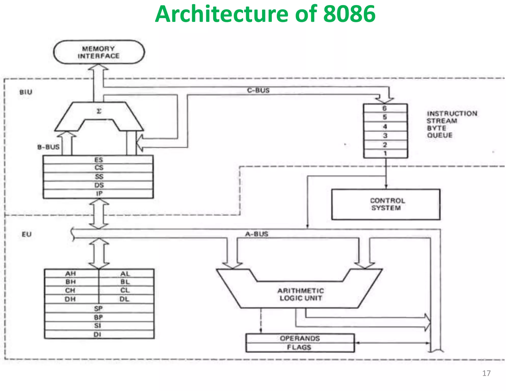
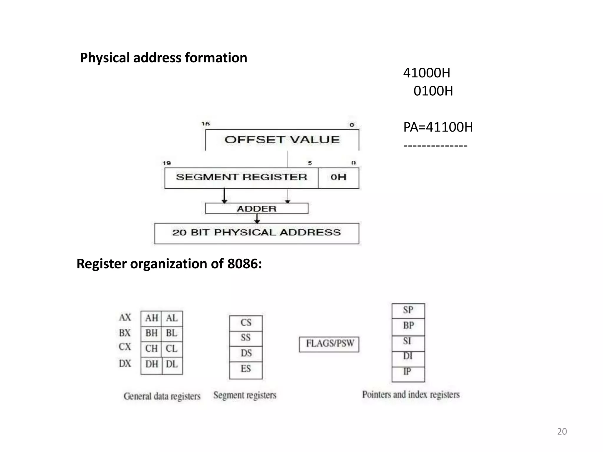
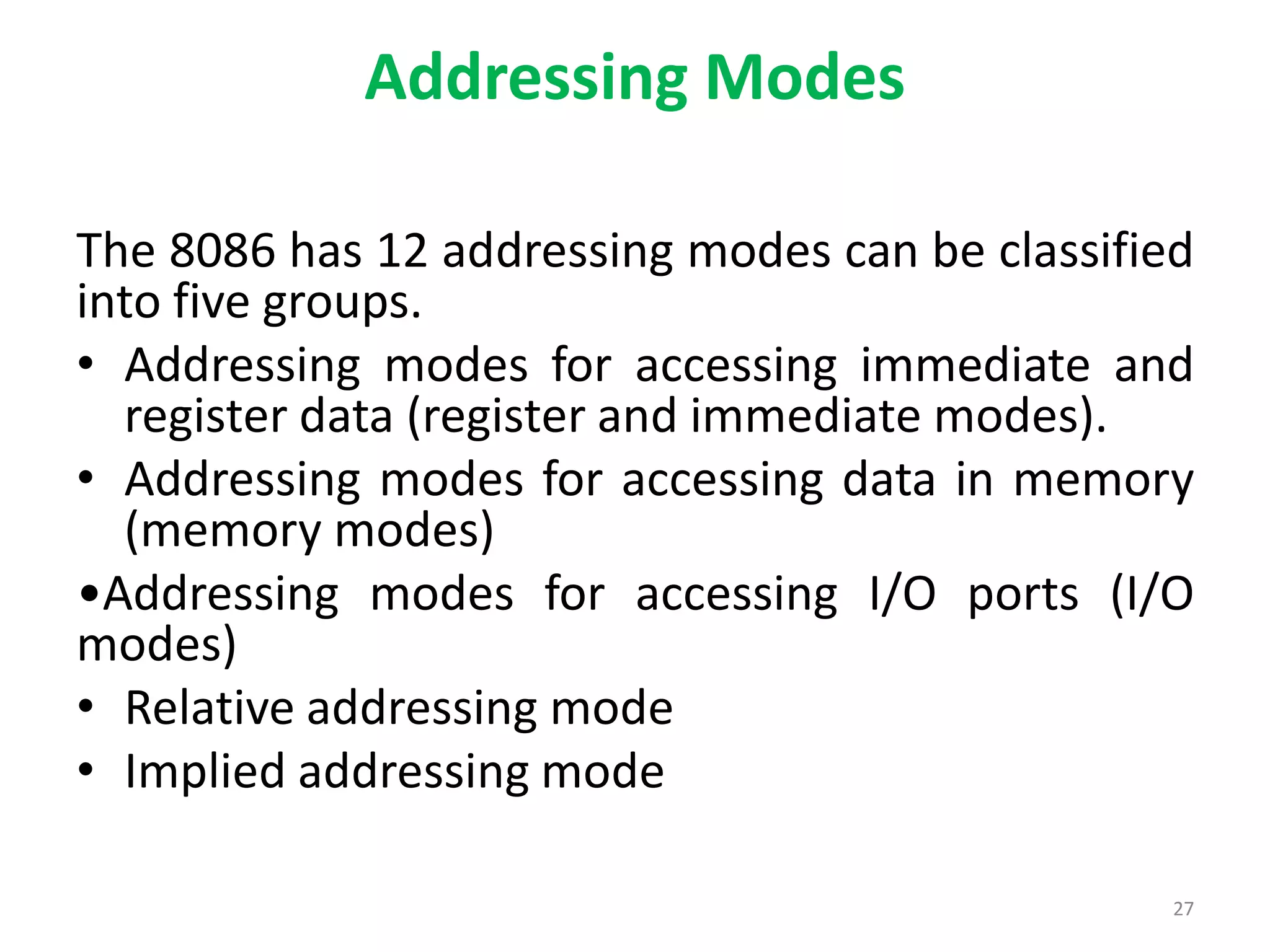
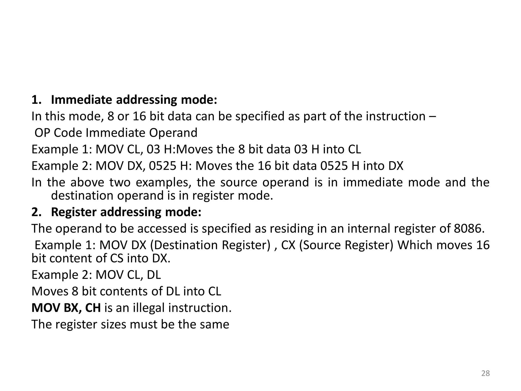
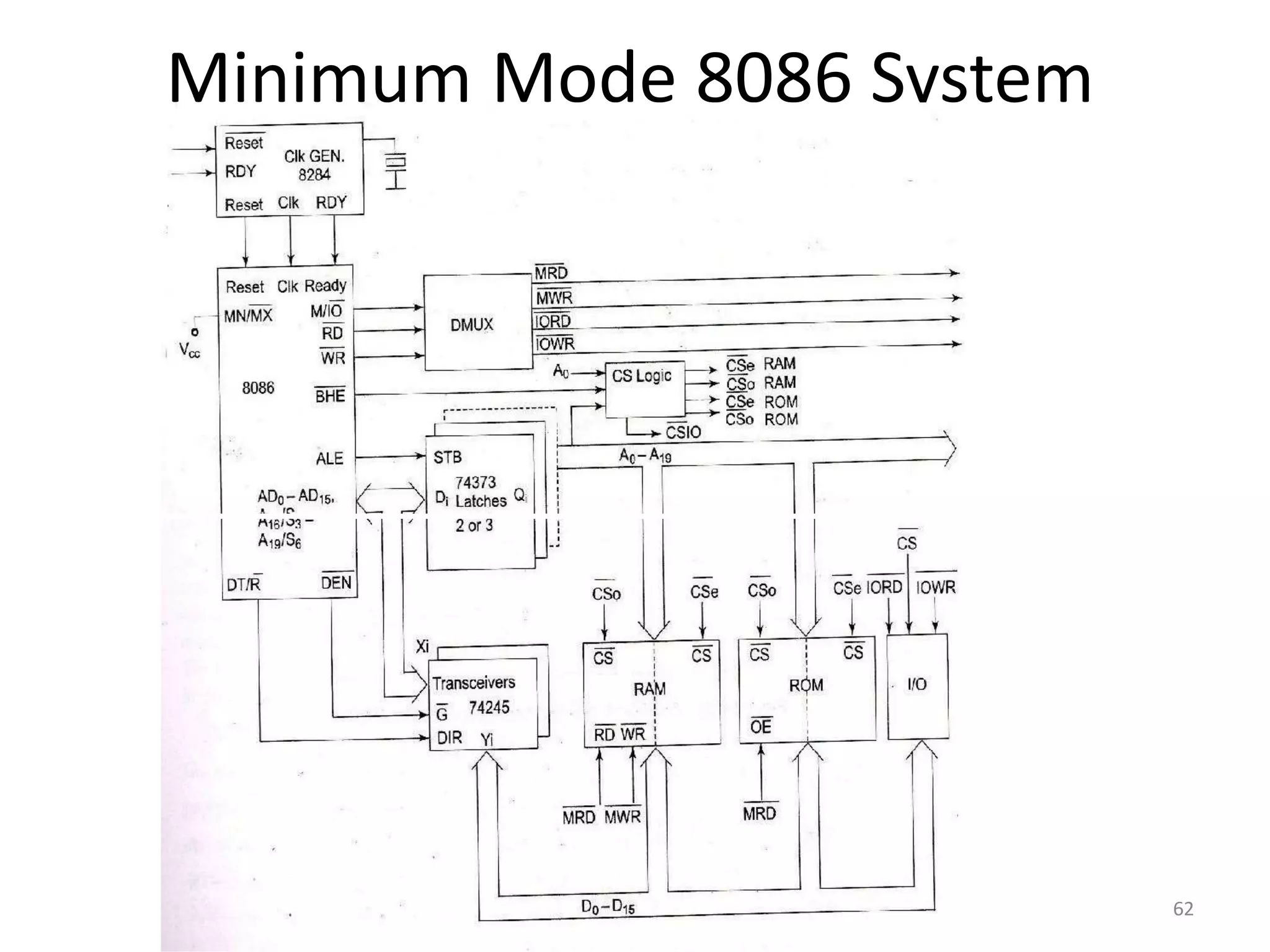
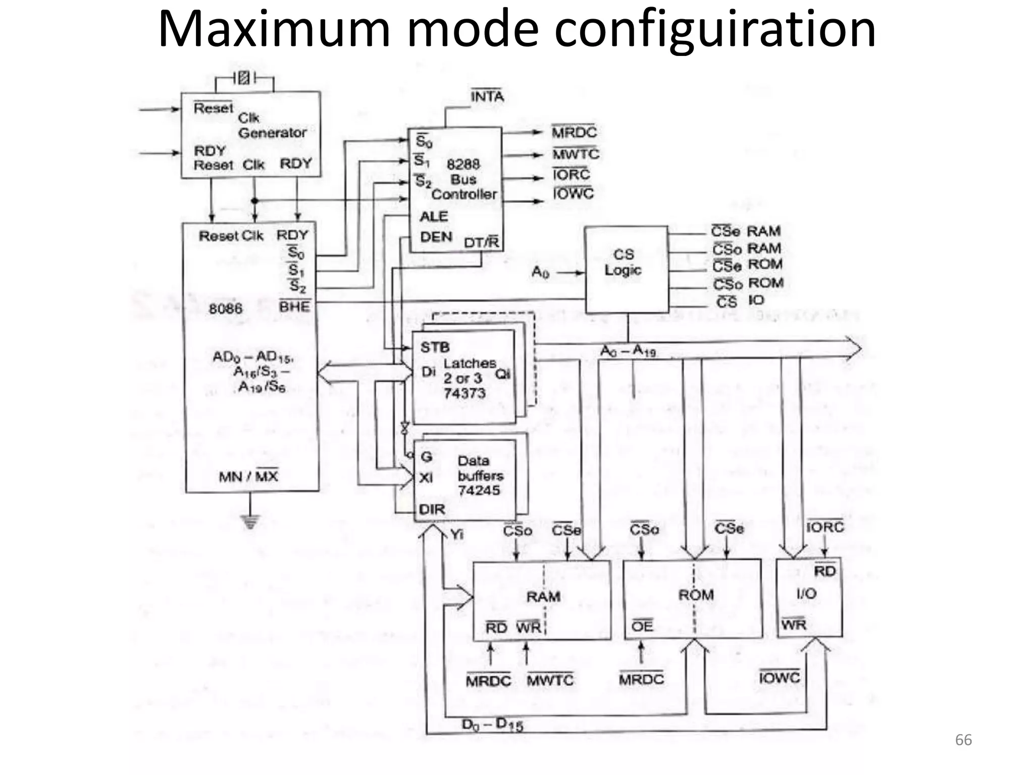
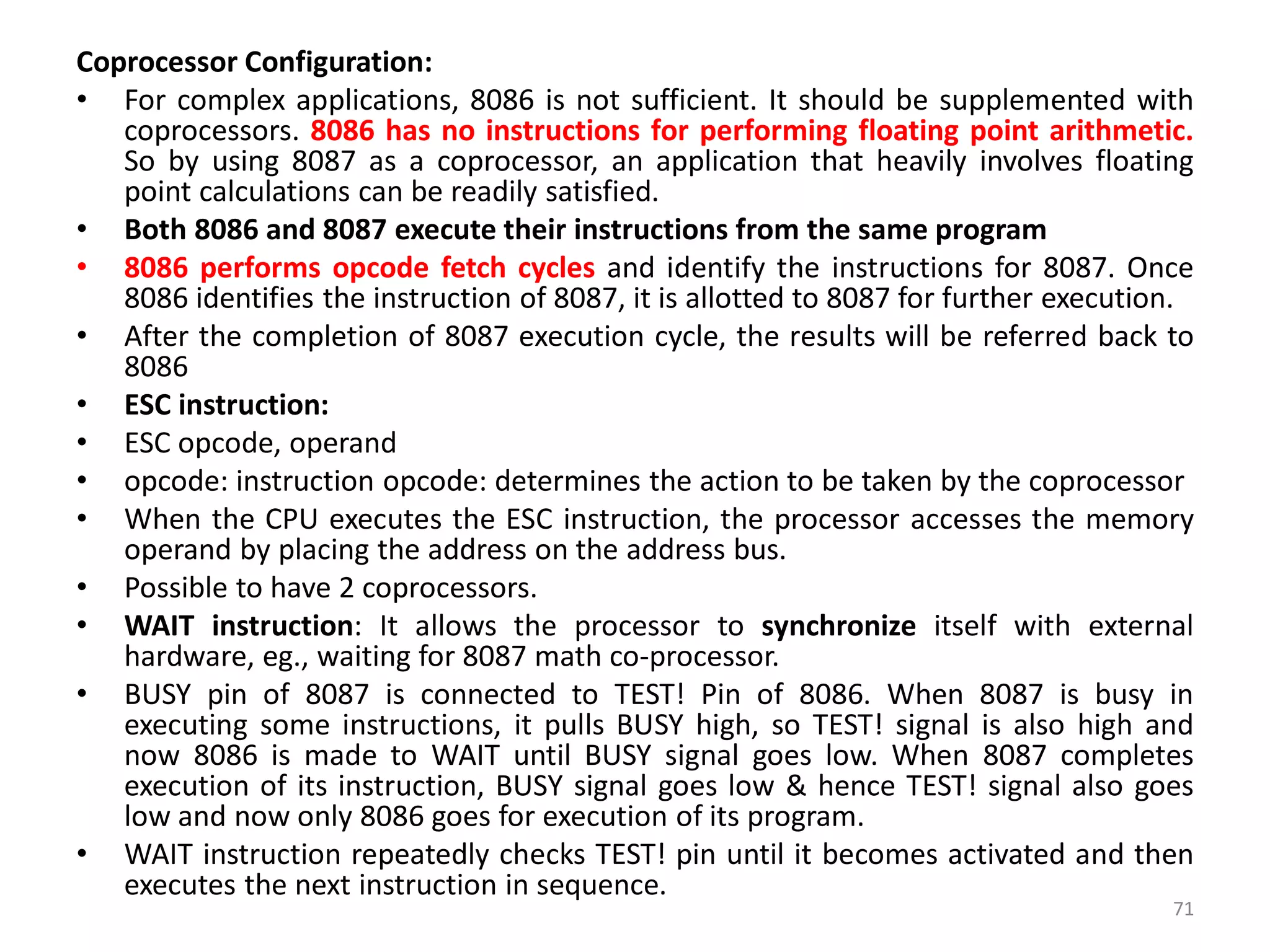
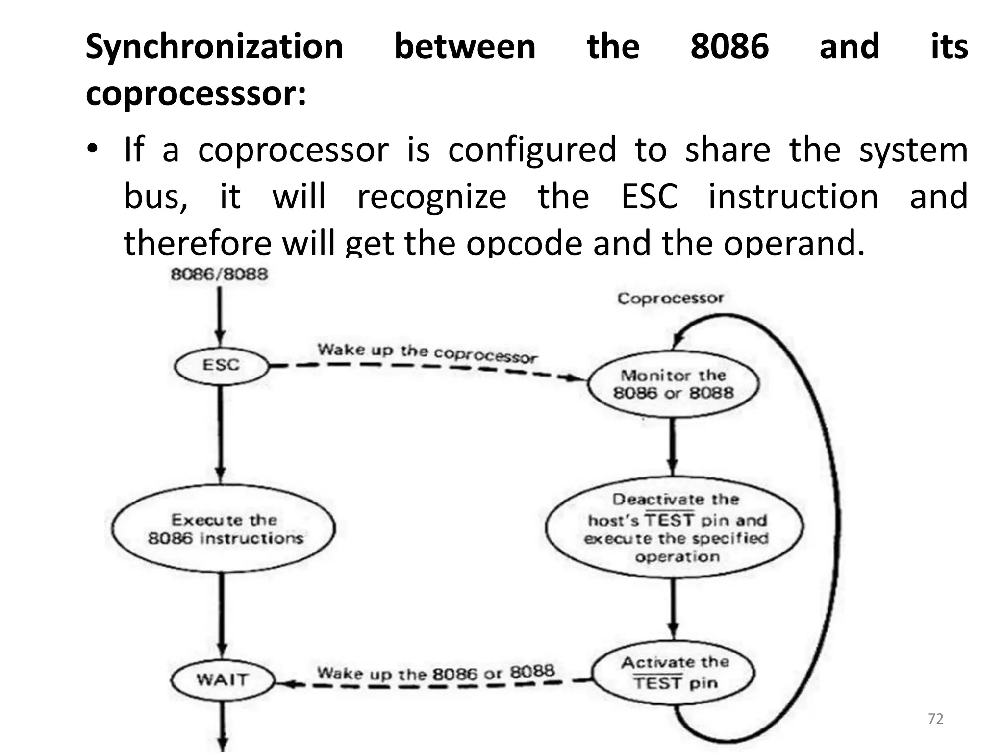
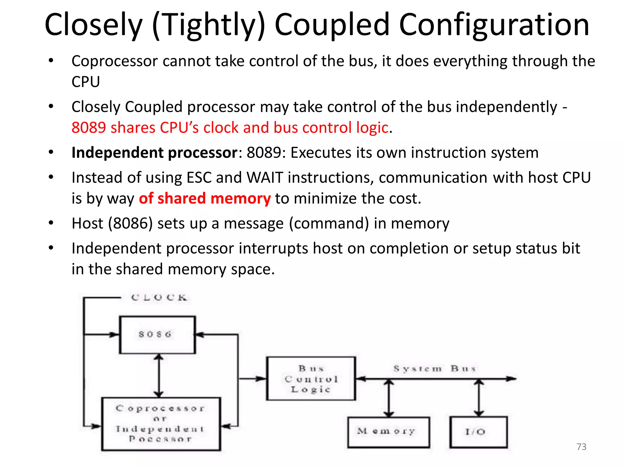
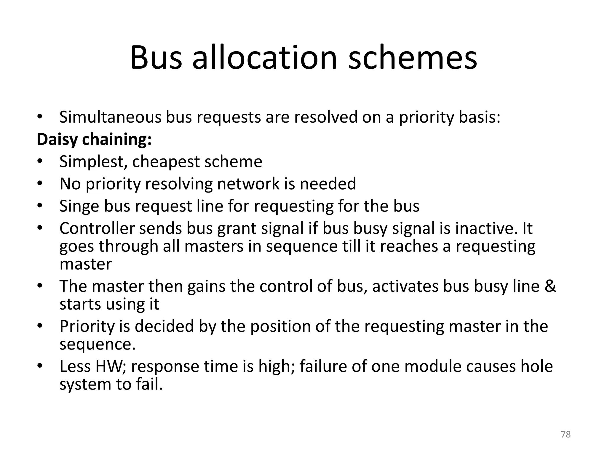
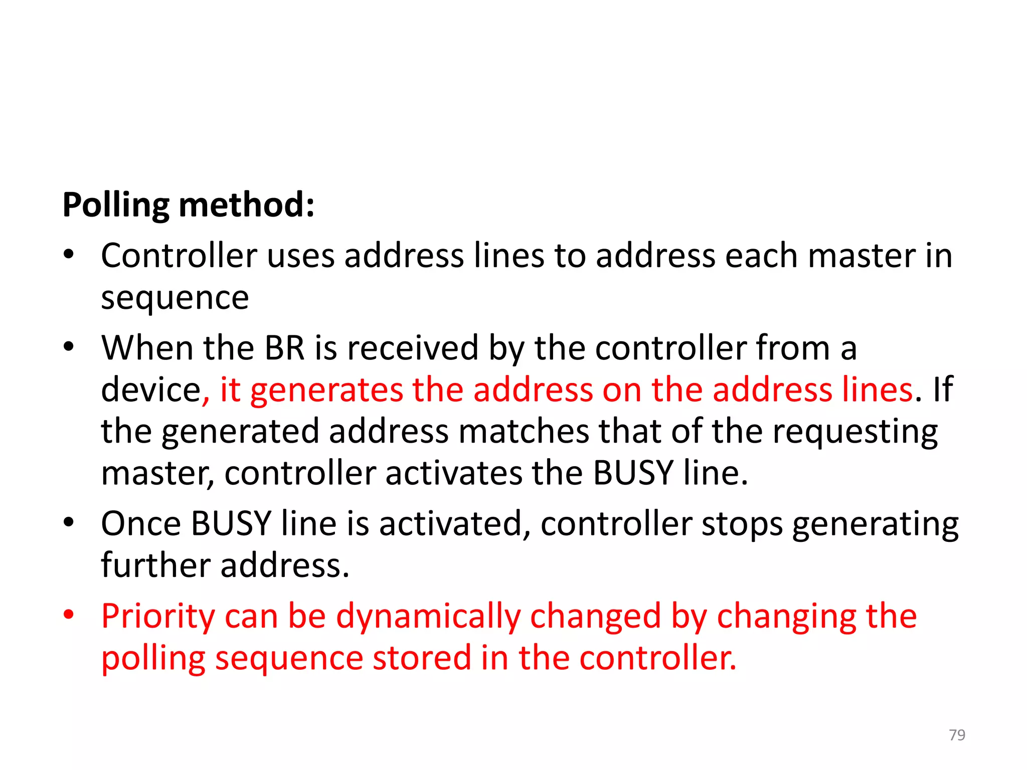
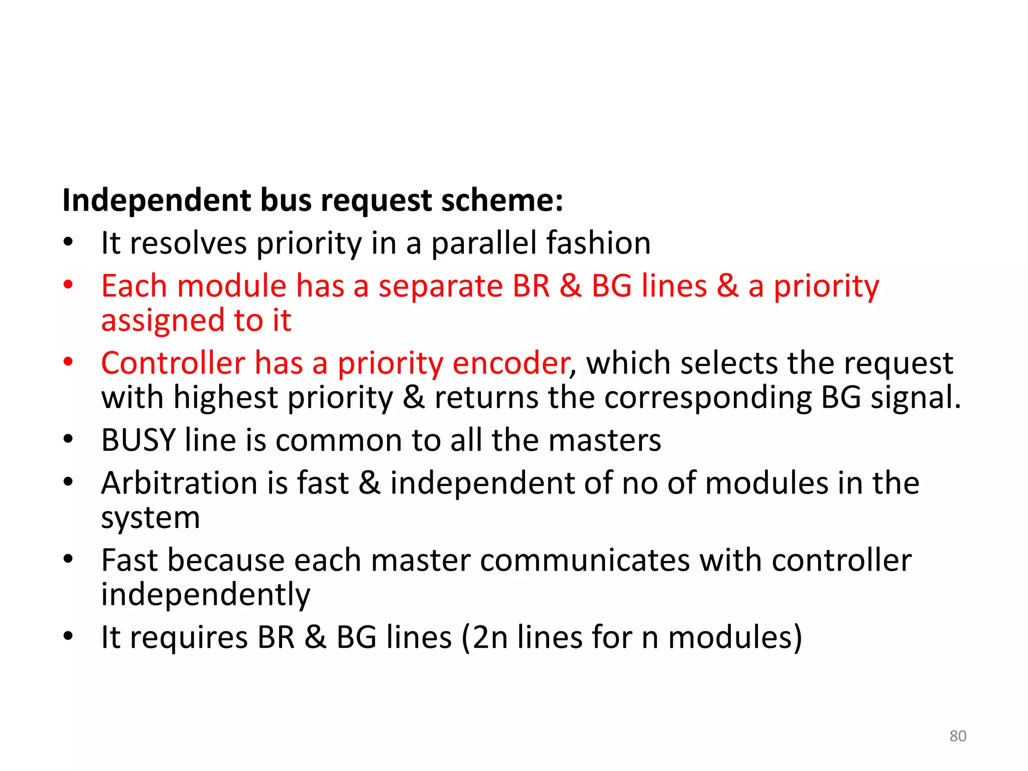
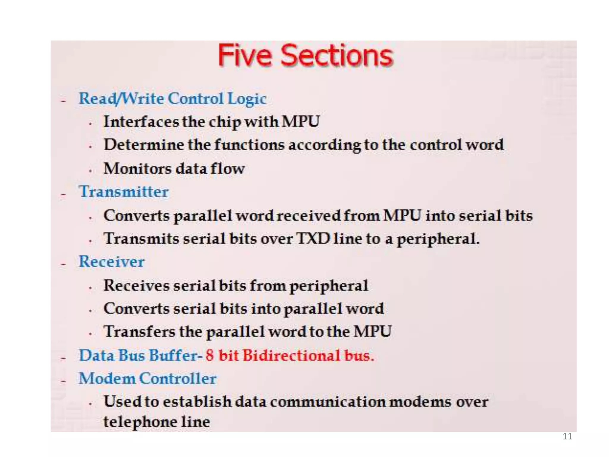
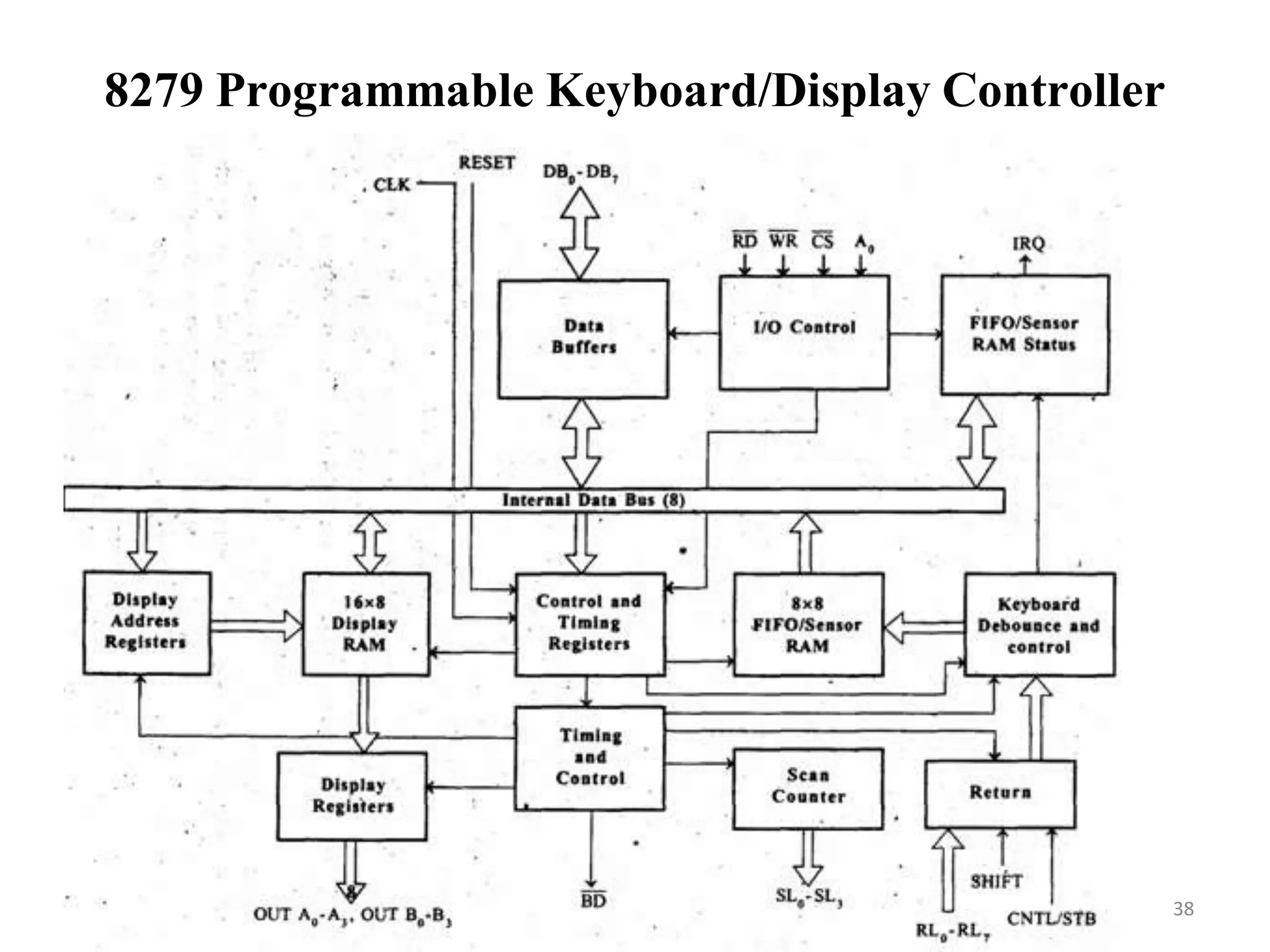
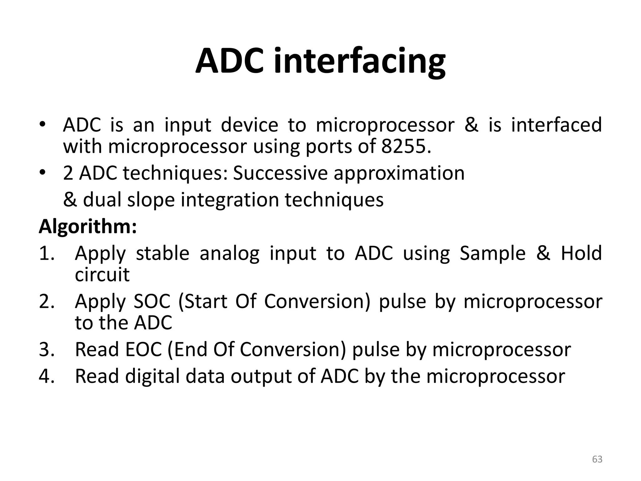
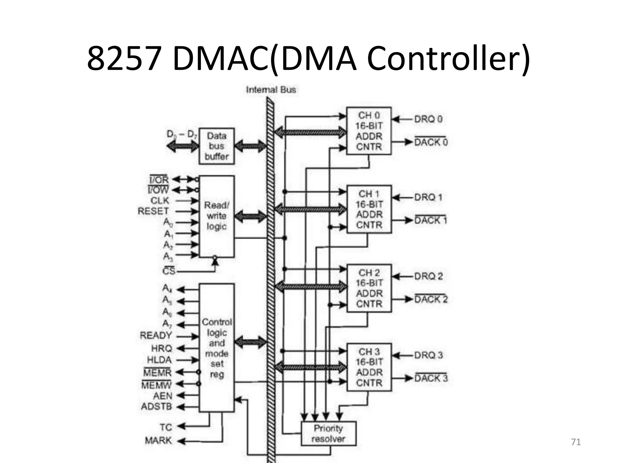
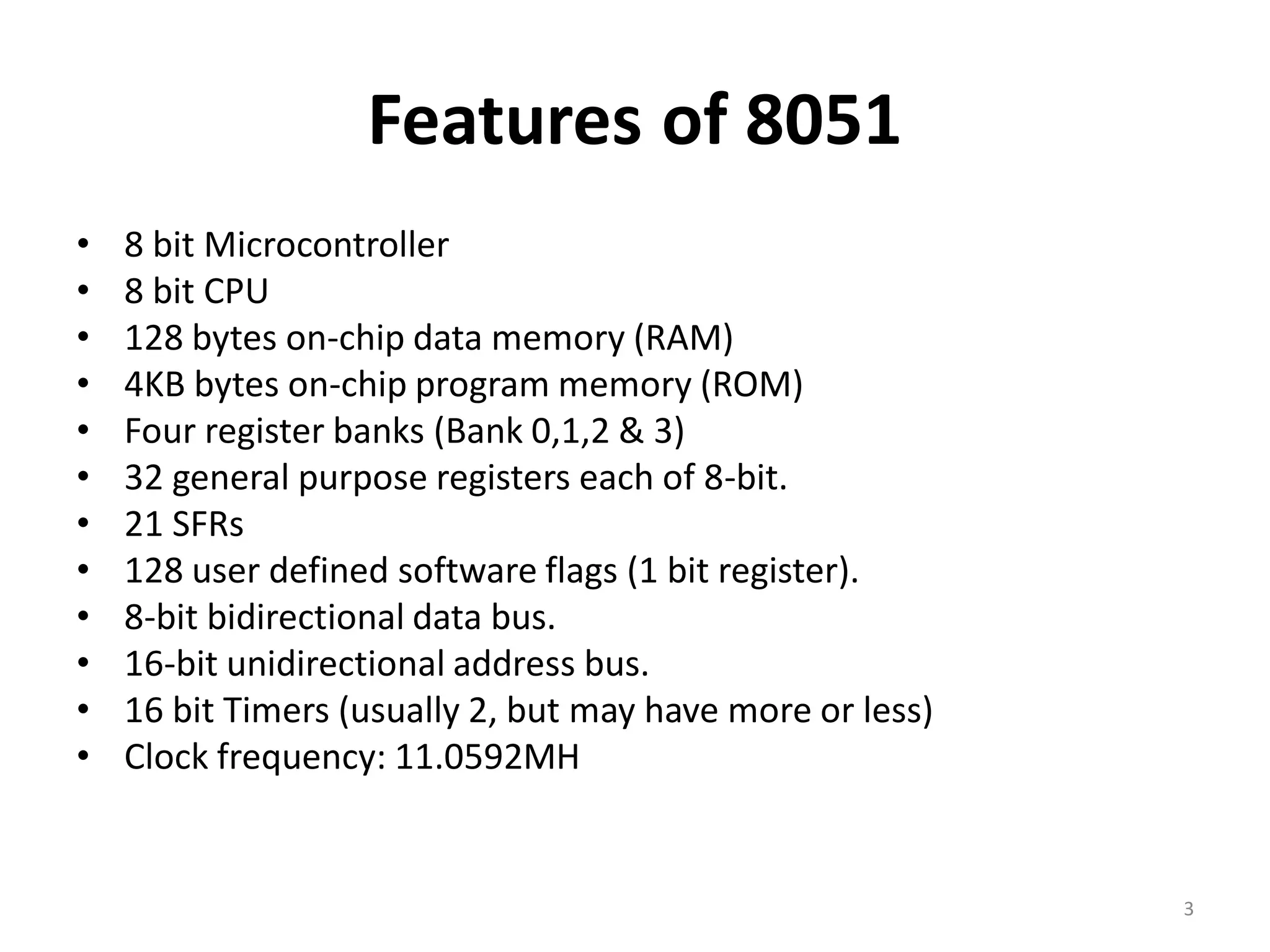
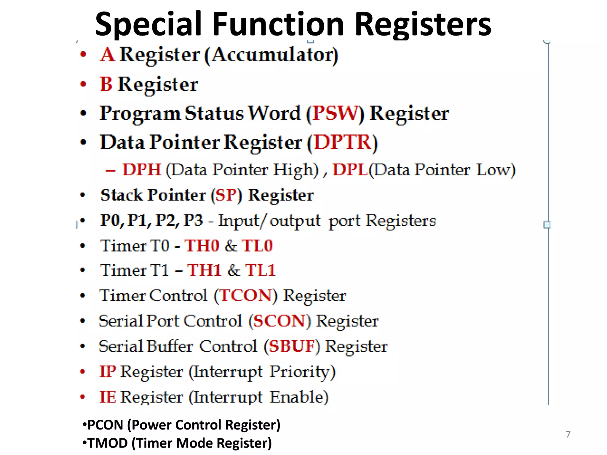
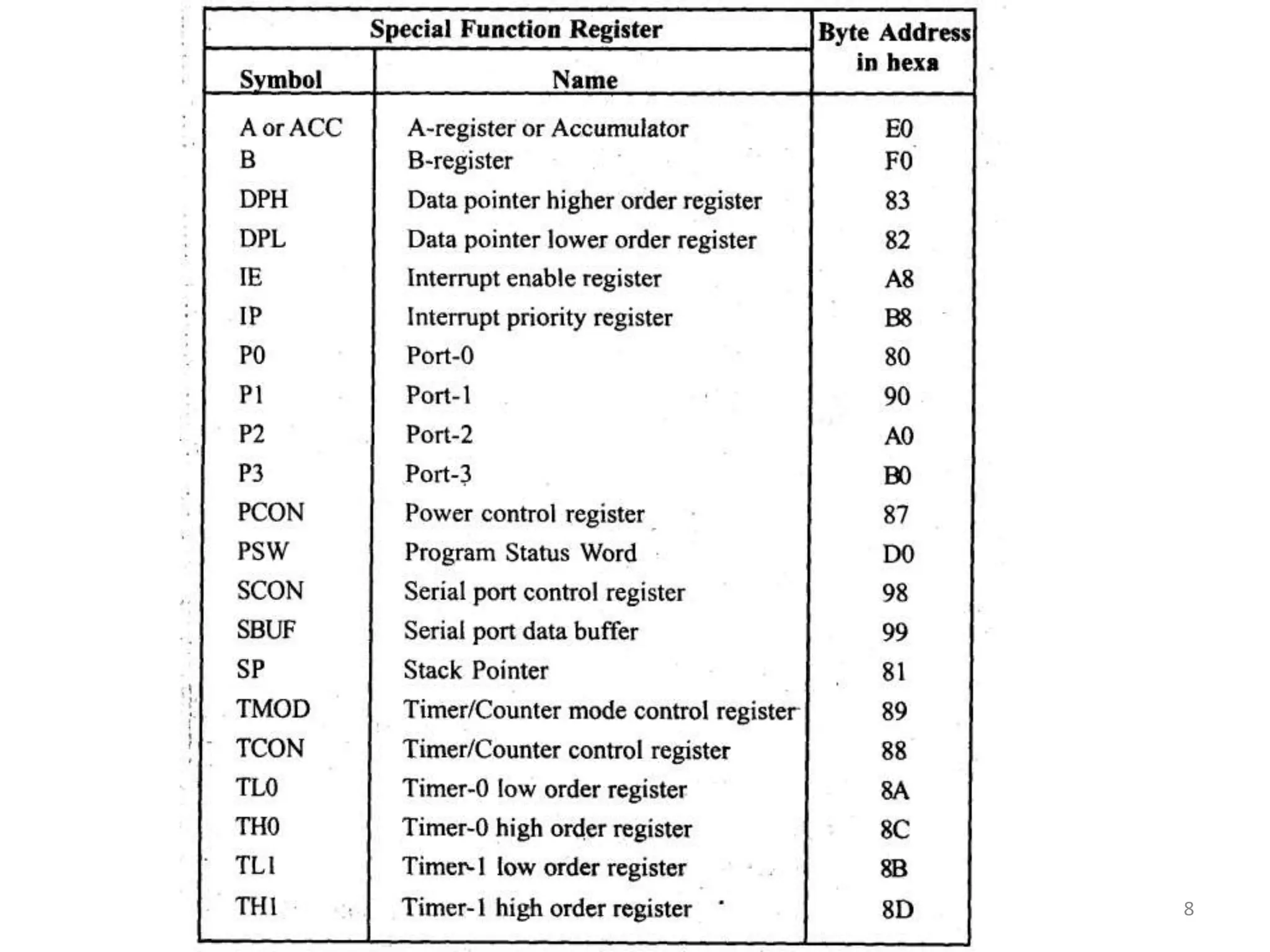
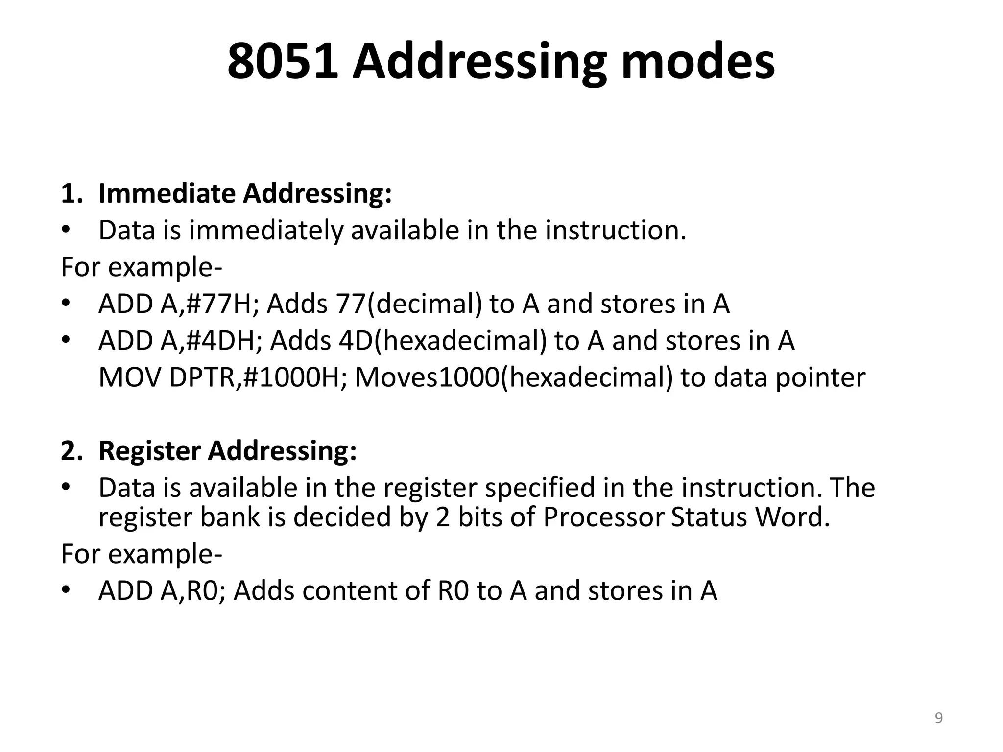
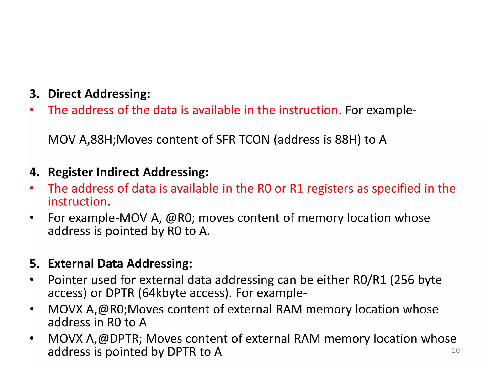
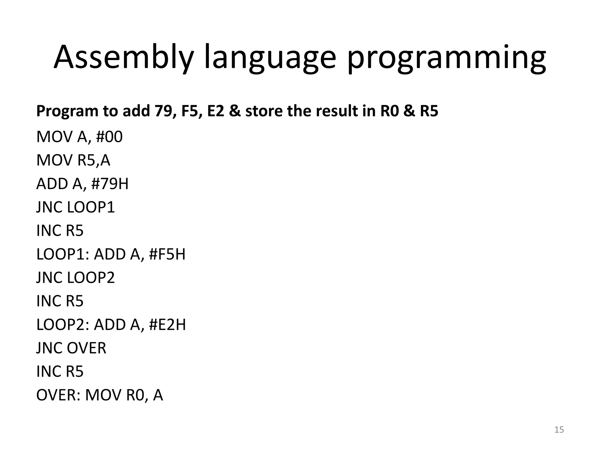
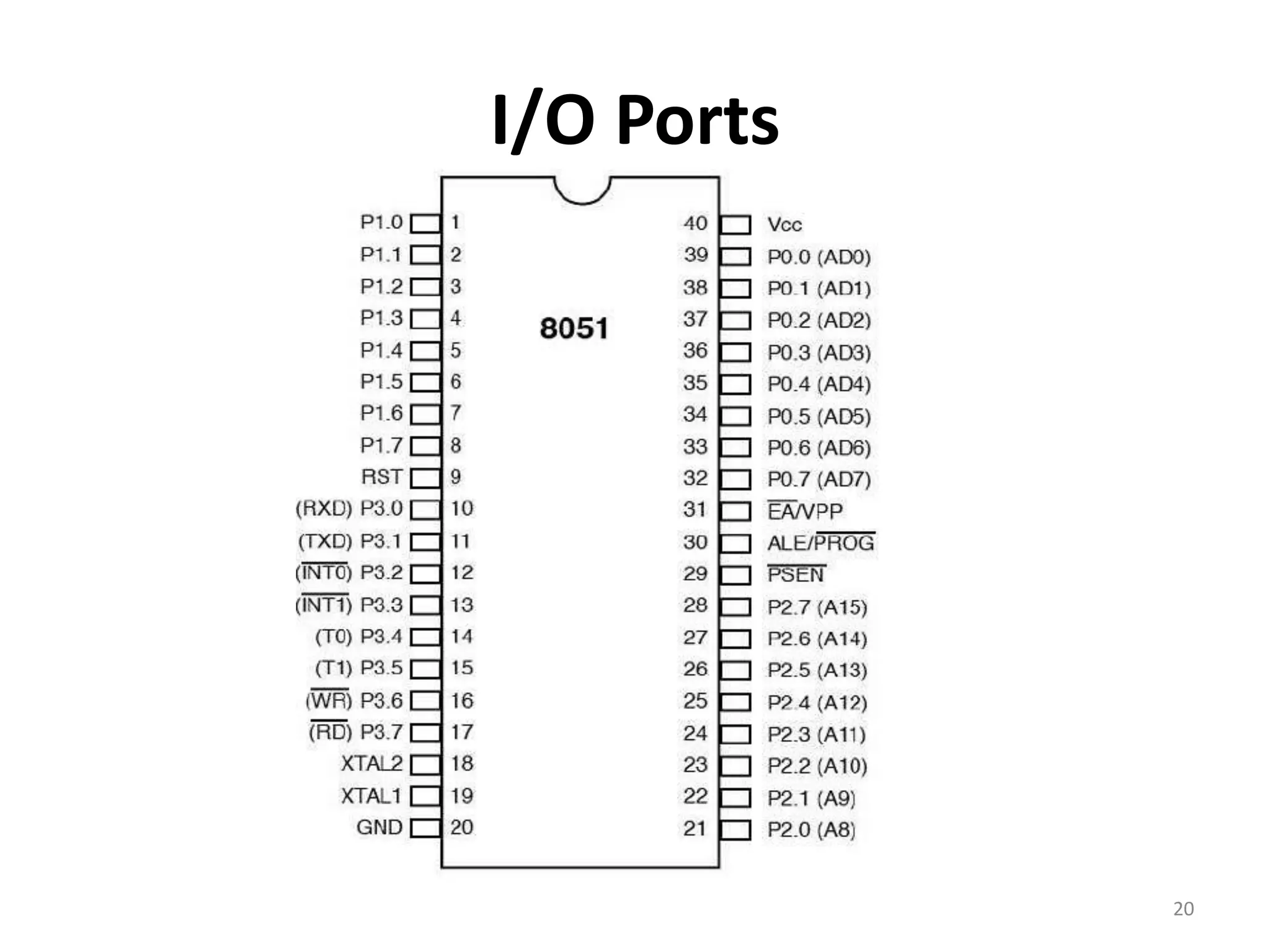
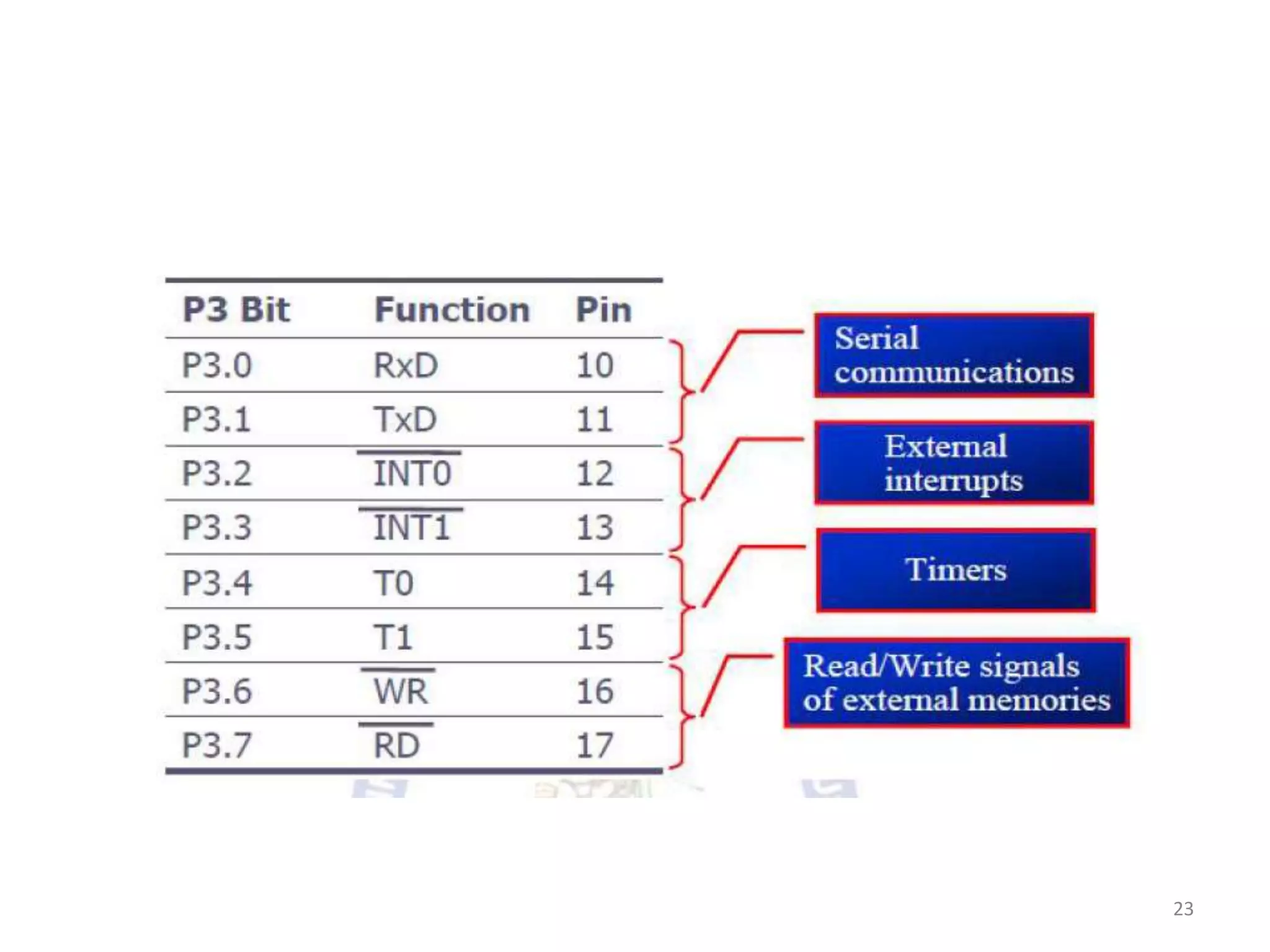
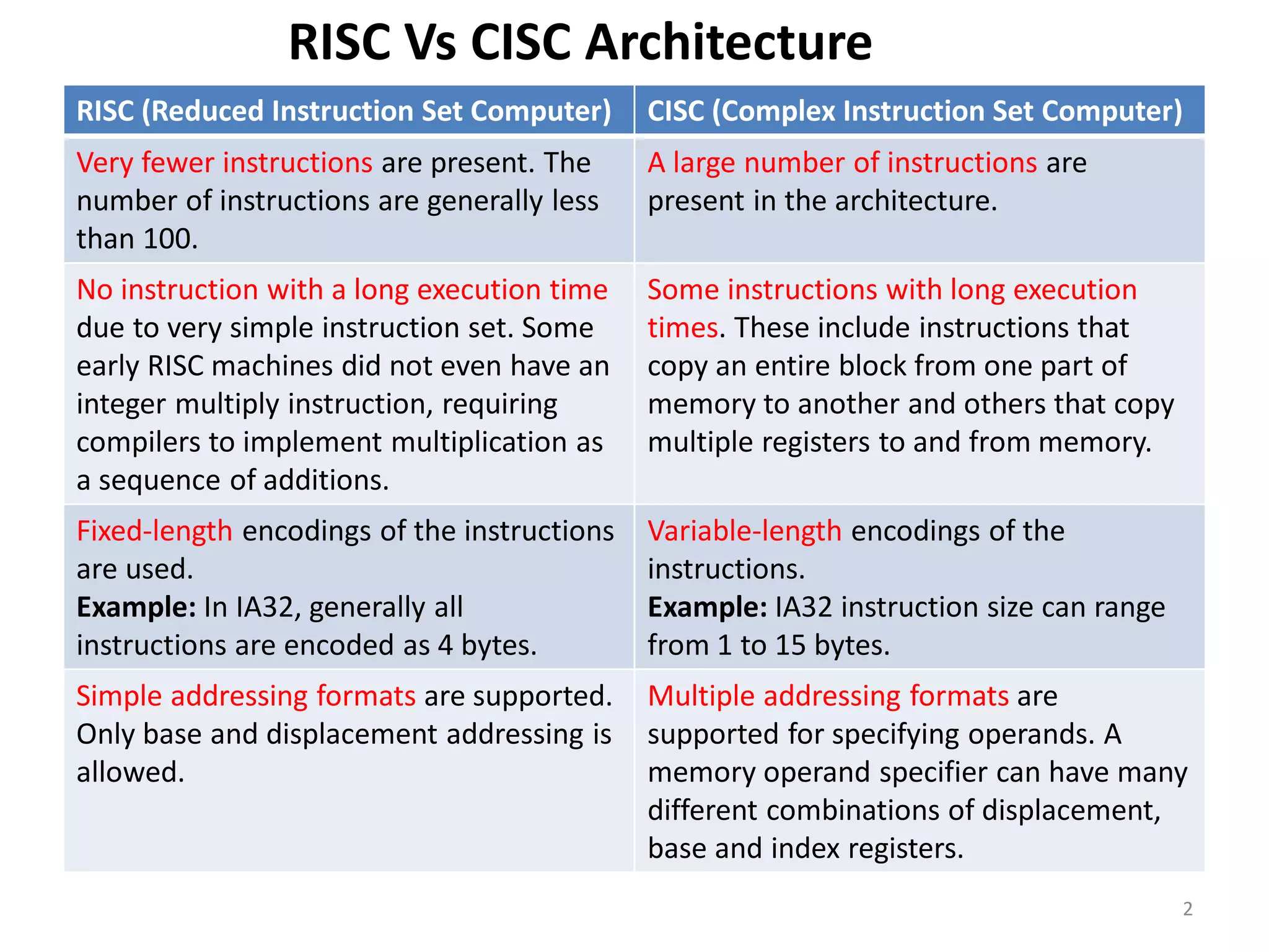
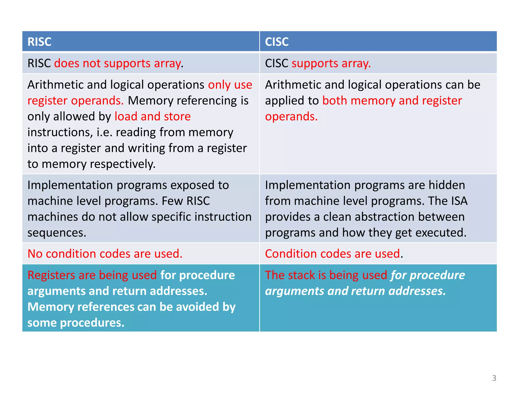
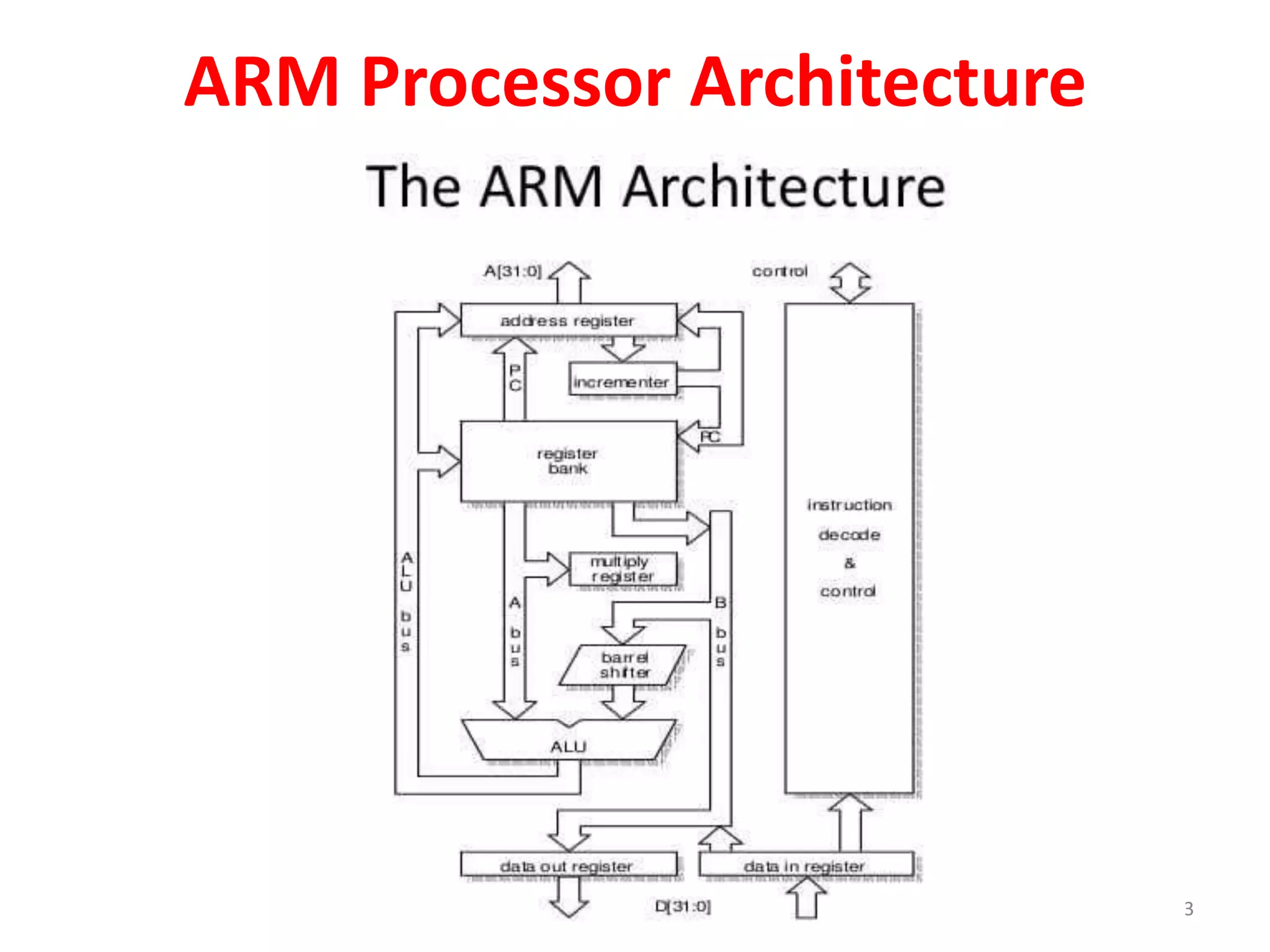
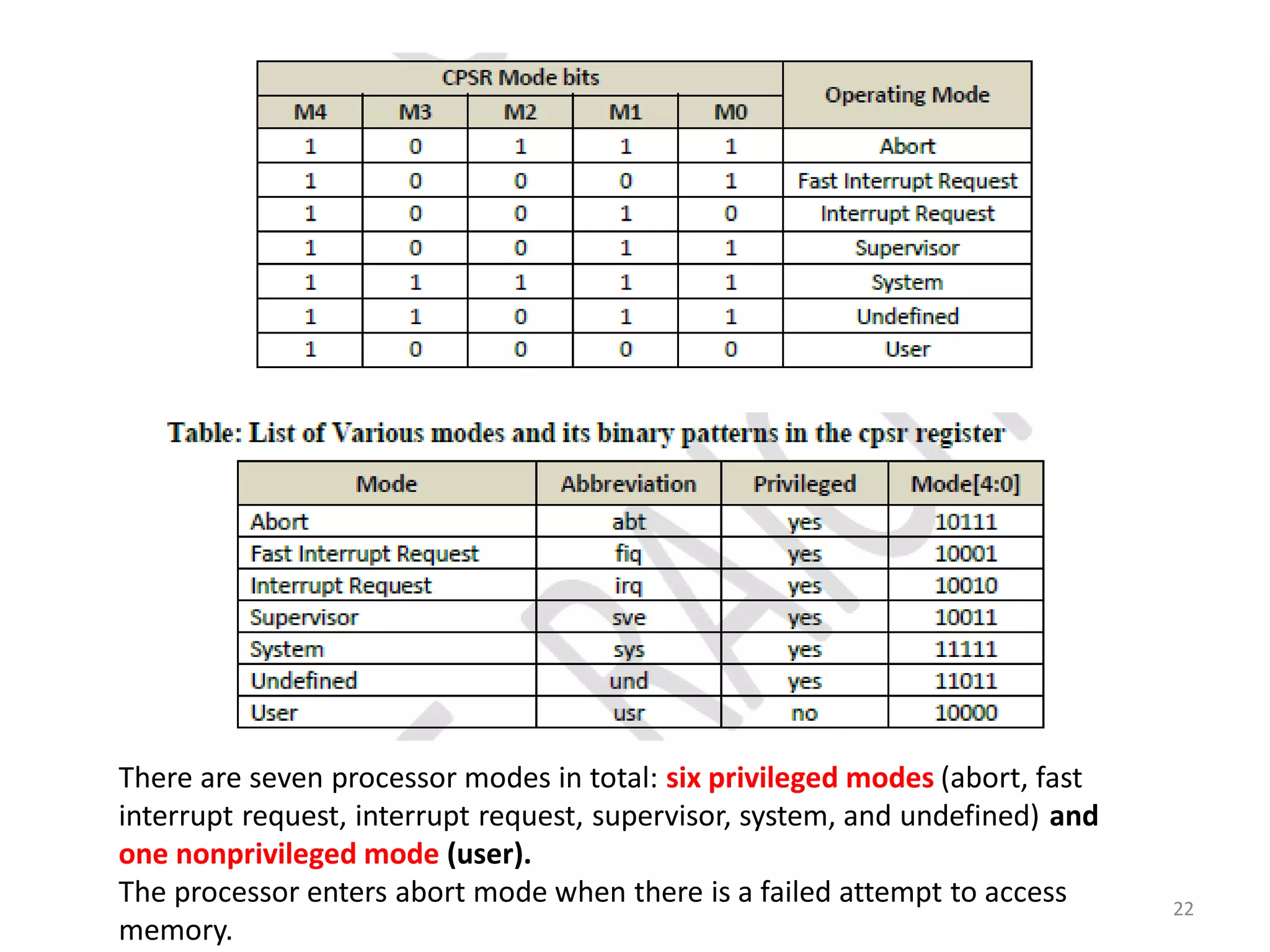
This document provides information about microprocessors and microcontrollers, specifically the 8085 and 8086 microprocessors. It discusses the architecture, features, registers, addressing modes, instruction sets and interrupts of the 8085 and 8086 microprocessors. The 8085 is an 8-bit microprocessor designed by Intel in 1977 using NMOS technology. The 8086 is a 16-bit microprocessor designed by Intel that can access 1 megabyte of memory and has 14 registers. Both microprocessors have various addressing modes including immediate, register, direct, indirect and relative modes.

![30
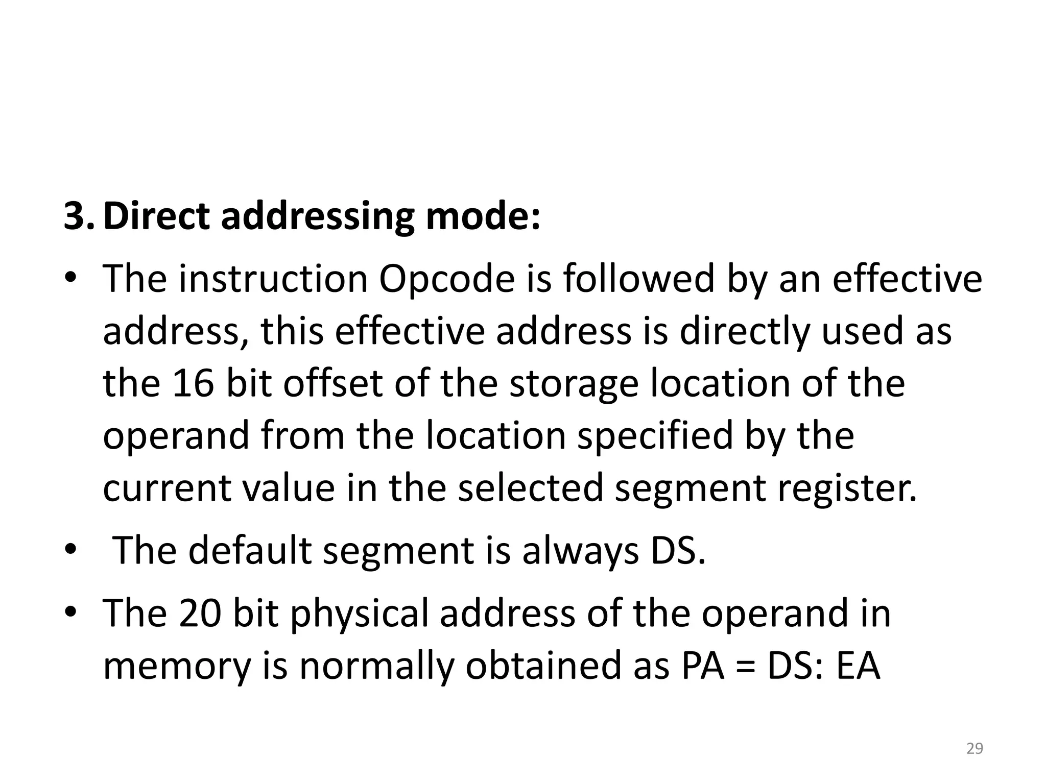
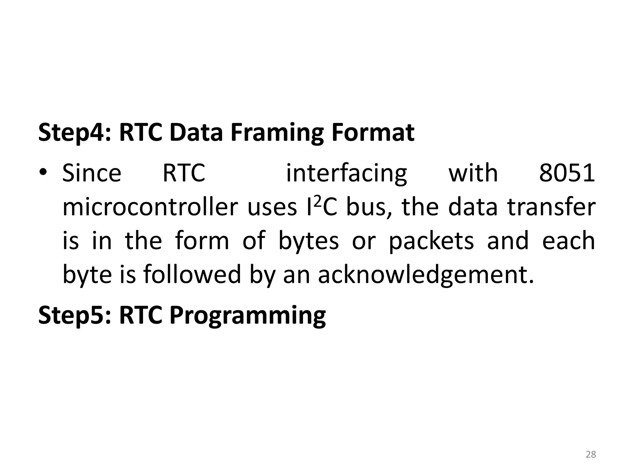
•In the direct addressing mode, the 16 bit effective address (EA)
is taken directly from the displacement field of the instruction.
Example 1: MOV CX, START
•If the 16 bit value assigned to the offset START by the
programmer using an assembler pseudo instruction such as DW
is 0040 and [DS] = 3050. Then BIU generates the 20 bit physical
address 30540 H.
The content of 30540 is moved to CL The content of 30541 is
moved to CH
Example 2: MOV CH, START
If [DS] = 3050 and START = 0040
8 bit content of memory location 30540 is moved to CH.
30500H
0040H
--------------
30540H=PA](https://image.slidesharecdn.com/chapter1merged-230928115840-bb6e9c62/75/MP_MC-pdf-30-2048.jpg)
![4. Register indirect addressing mode:
• The EA is specified in either pointer (BX) register or an index (SI or
DI) register. The 20 bit physical address is computed using DS and
EA.
• Example: MOV [DI], BX
If [DS] = 5004, [DI] = 0020, [Bx] = 2456 PA=50060.
The content of BX (2456) is moved to memory locations 50060 H and
50061 H.
31](https://image.slidesharecdn.com/chapter1merged-230928115840-bb6e9c62/75/MP_MC-pdf-31-2048.jpg)
![5. Based addressing mode:
• When memory is accessed PA is computed from BX and DS
when the stack is accessed PA is computed from BP and SS.
• Example: MOV AL, START [BX] or
MOV AL, [START + BX]
In based mode
• EA: [START] + [BX]
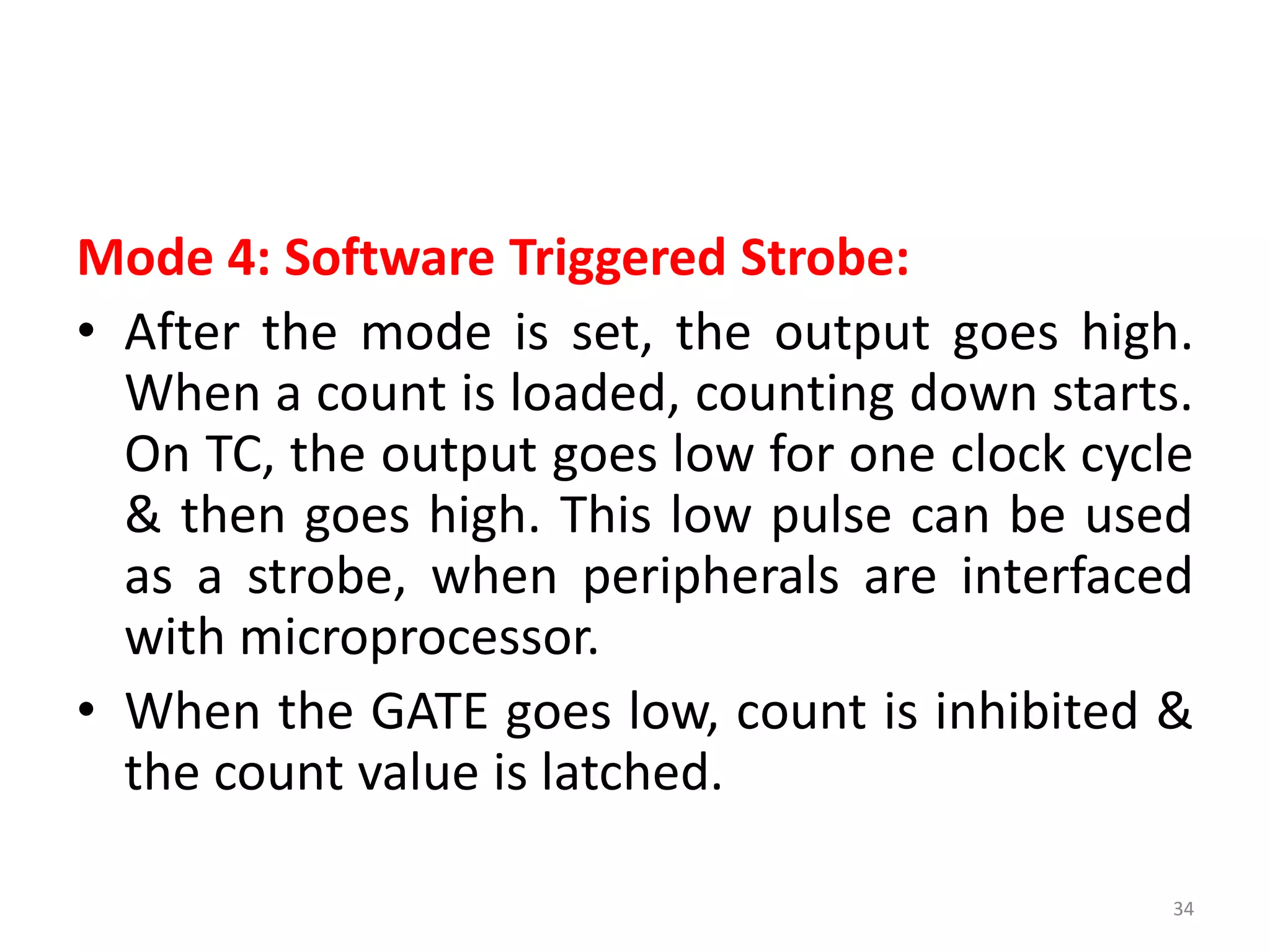
• PA: [DS] + [EA]
• The 8 bit content of this memory location is moved to AL.
32](https://image.slidesharecdn.com/chapter1merged-230928115840-bb6e9c62/75/MP_MC-pdf-32-2048.jpg)
![6. String addressing mode:
• The string instructions automatically assume SI to point to
the first byte or word of the source operand and DI to point
to the first byte or word of the destination operand. The
contents of SI and DI are automatically incremented (by
clearing DF to 0 by CLD instruction) to point to the next
byte or word.
• Example: MOV S BYTE
• If [DF] = 0, [DS] = 2000 H, [SI] = 0500, [ES] = 4000,
[DI] = 0300
• Source address: PA= [DS] + [SI]=20500
• Destination address: PA=[ES] + [DI] = 40300
33](https://image.slidesharecdn.com/chapter1merged-230928115840-bb6e9c62/75/MP_MC-pdf-33-2048.jpg)
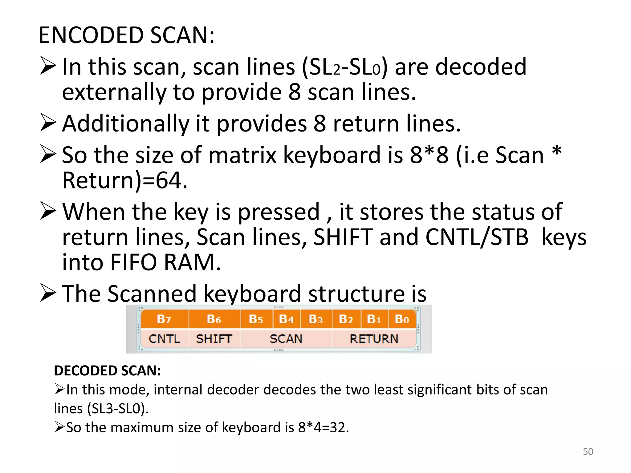
![9. I/O mode (direct):
• Port number is an 8 bit immediate operand. Example: OUT 05 H, AL
• Outputs [AL] to 8 bit port 05 H
10. I/O mode (indirect):
• The port number is taken from DX. Example 1: IN AL, DX
• If [DX] = 5040
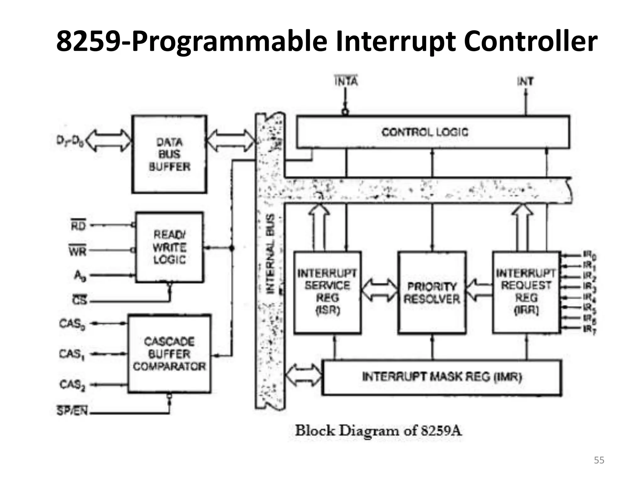
• 8 bit content from port 5040 is moved into AL.
• Example 2: IN AX, DX
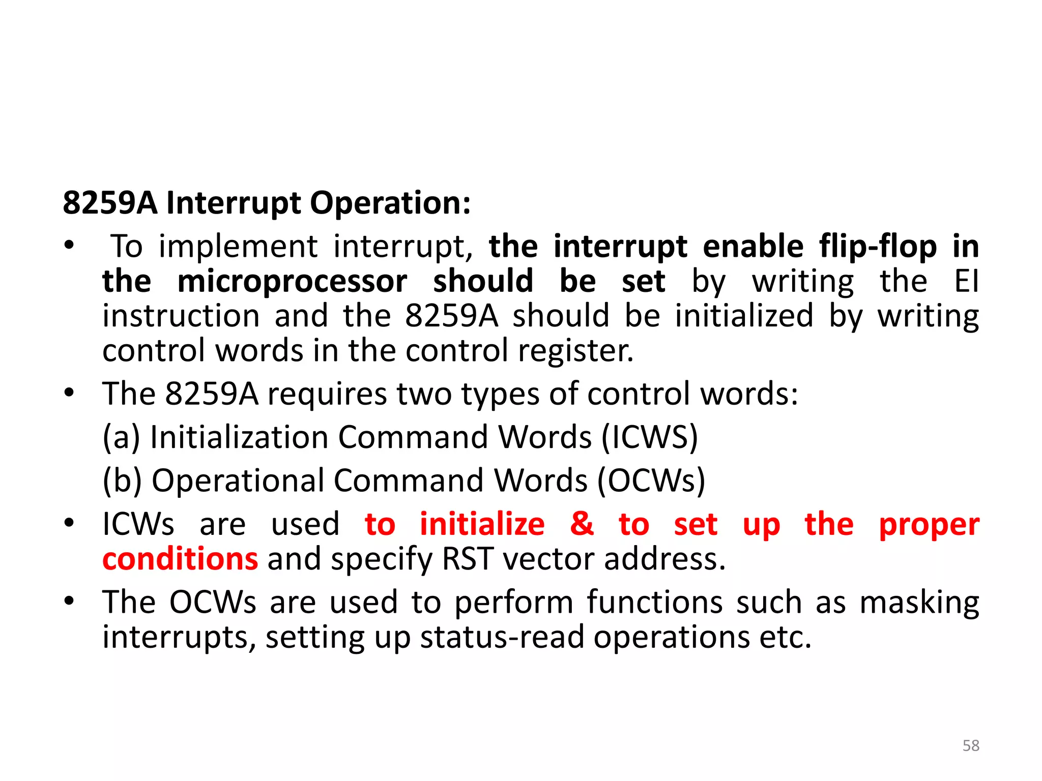
• Inputs 8 bit content of ports 5040 and 5041 into AL and AH respectively.
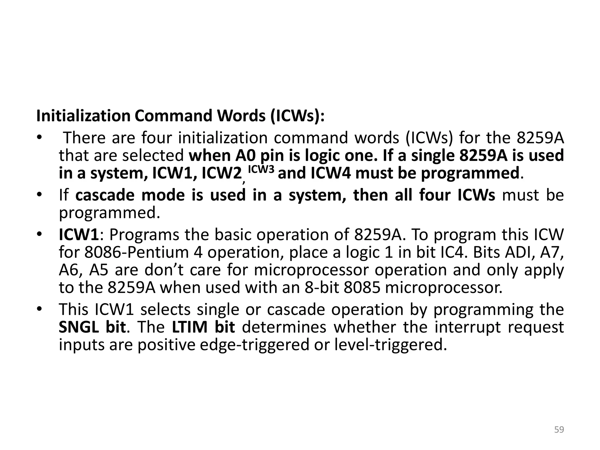
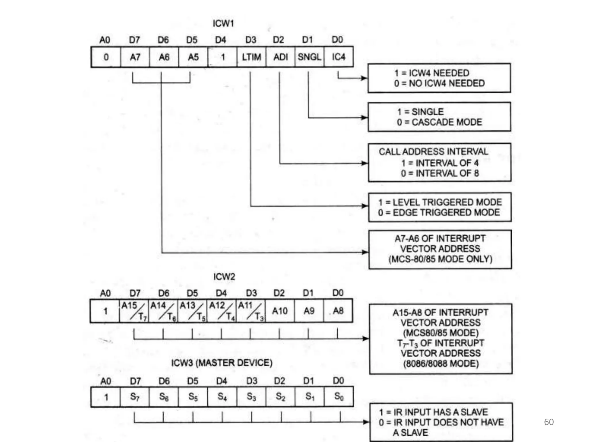
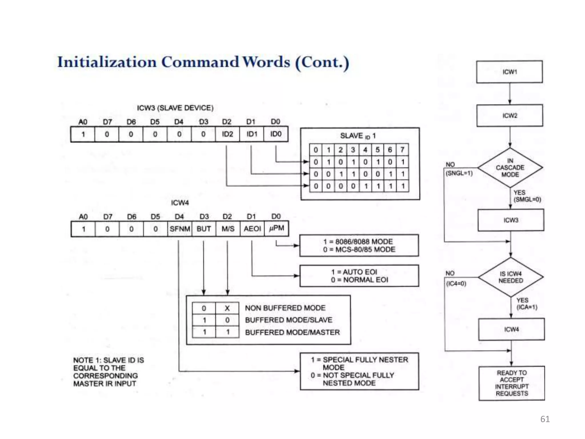
11. Relative addressing mode:
• Example: JNC START
• If CY=O, then PC is loaded with current PC contents plus 8 bit signed value
of START, otherwise the next instruction is executed.
12. Implied addressing mode:
• Instruction using this mode has no operands.
• Example: CLC which clears carry flag to zero.
35](https://image.slidesharecdn.com/chapter1merged-230928115840-bb6e9c62/75/MP_MC-pdf-35-2048.jpg)
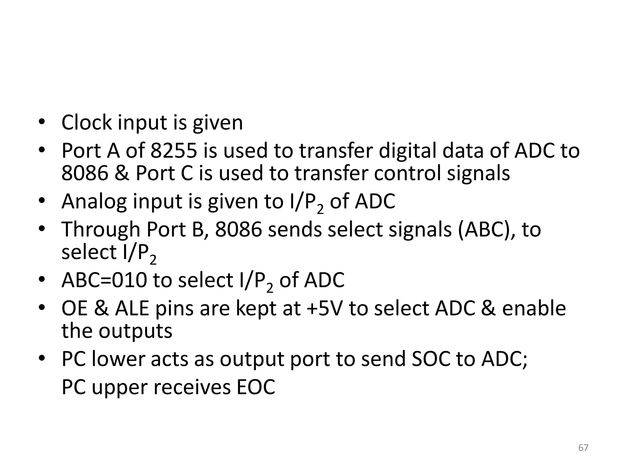
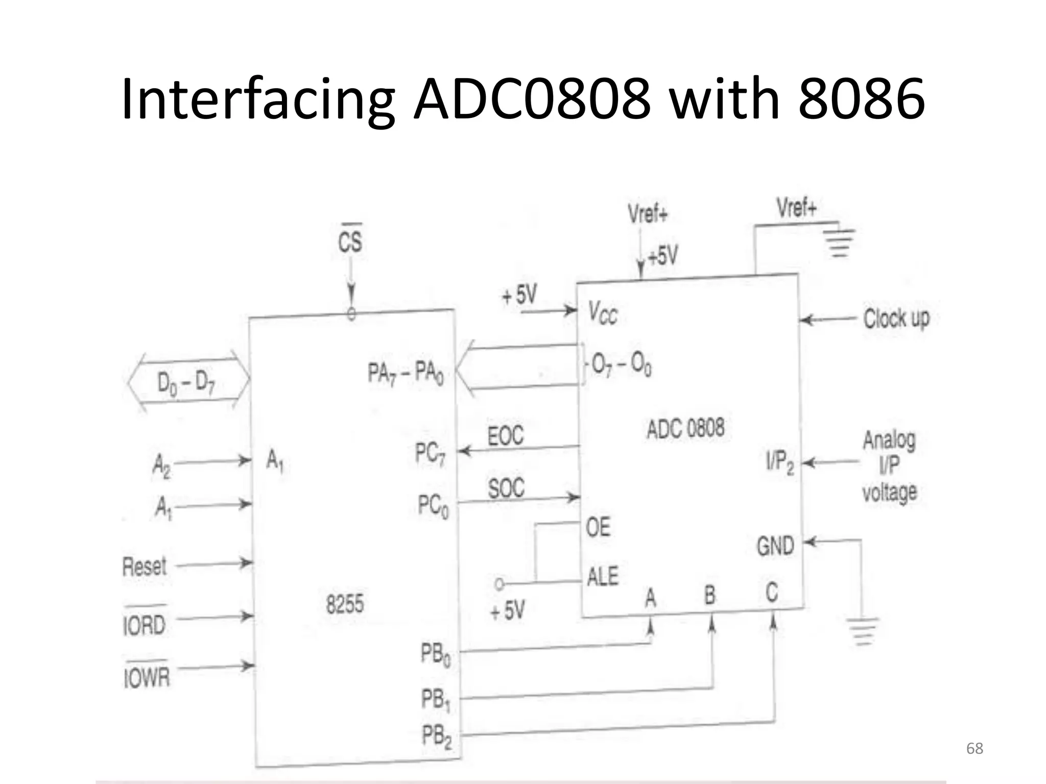
![• Data Copy / Transfer Instructions:
• MOV:This instruction copies a word or a byte of data from some source to
a destination. The destination can be a register or a memory location. The
source can be a register, a memory location, or an immediate number.
• MOV AX, BX
• MOV AX, 5000H
• MOV AX, [SI]
• MOV AX, [2000H]
• MOV AX, 50H[BX]
• MOV [734AH], BX
• MOV DS, CX
• MOV CL, [357AH]
PUSH: Push to Stack
• This instruction pushes the contents of the specified register/memory
location on to the stack. The stack pointer is decremented by 2, after each
execution of the instruction.
E.g. PUSH AX
PUSH DS
PUSH [5000H]
37](https://image.slidesharecdn.com/chapter1merged-230928115840-bb6e9c62/75/MP_MC-pdf-37-2048.jpg)
![POP: Pop from Stack
• This instruction when executed, loads the specified
register/memory location with the
• contents of the memory location of which the address is formed
using the current stack
• segment and stack pointer.
• The stack pointer is incremented by 2 Eg. POP AX
• POP DS
• POP [5000H]
XCHG: Exchange byte or word
• This instruction exchange the contents of the specified source and
destination operands
• Eg. XCHG [5000H], AX
38](https://image.slidesharecdn.com/chapter1merged-230928115840-bb6e9c62/75/MP_MC-pdf-38-2048.jpg)
![• XCHG BX, AX
• Input and output port transfer instructions: IN:Copy a byte
or word from specified port to accumulator.
• Eg. IN AL,03H
• IN AX,DX
• OUT:Copy a byte or word from accumulator specified port.
• Eg. OUT 03H, AL
• OUT DX, AX
• LEA:Load effective address of operand in specified register.
[reg] offset portion of address in DS
• Eg. LEA reg, offset
• LDS: Load DS register and other specified register from
memory.
• [reg] [mem]
• [DS] [mem + 2]
• Eg. LDS reg, mem
39](https://image.slidesharecdn.com/chapter1merged-230928115840-bb6e9c62/75/MP_MC-pdf-39-2048.jpg)
![Flag transfer instructions: LAHF:
• Load (copy to) AH with the low byte the flag register
• Eg. LAHF
• SAHF:
• Store (copy) AH register to low byte of flag register.
• Eg. SAHF
• PUSHF:
• Copy flag register to top of stack. [SP]= [SP] – 2
• [[SP]] [Flags]
• Eg. PUSHF
• POPF:
• Copy word at top of stack to flag register. [Flags] [[SP]]
• [SP]= [SP] + 2
40](https://image.slidesharecdn.com/chapter1merged-230928115840-bb6e9c62/75/MP_MC-pdf-40-2048.jpg)
![Arithmetic operations:
• Addition, subtraction, negation, multiplication and comparing two
values.
ADD:
• The add instruction adds the contents of the source operand to the
destination operand.
• Eg. ADD AX, 0100H
• ADD AX, BX
• ADD AX, [SI]
• ADD AX, [5000H]
• ADD [5000H], 0100H
ADC: Add with Carry
• This instruction performs the same operation as ADD instruction,
but adds the carry flag to the result.
• Eg.
• ADC AX, BX
• ADC AX, [SI]
• ADC AX, [5000]
• ADC [5000], 0100H
41](https://image.slidesharecdn.com/chapter1merged-230928115840-bb6e9c62/75/MP_MC-pdf-41-2048.jpg)
![• SUB: Subtract
• The subtract instruction subtracts the source operand from
the destination operand and the result is left in the
destination operand.
• Eg. SUB AX, 0100H
• SUB AX, BX
• SUB AX, [5000H]
• SUB [5000H], 0100H
• SBB: Subtract with Borrow
• The subtract with borrow instruction subtracts the source
operand and the borrow flag (CF) which may reflect the
result of the previous calculations, from the destination
operand
• Eg. SBB AX, 0100H
• SBB AX, BX
• SBB AX, [5000H]
• SBB [5000H], 0100H
42](https://image.slidesharecdn.com/chapter1merged-230928115840-bb6e9c62/75/MP_MC-pdf-42-2048.jpg)
![• INC: Increment
• This instruction increases the contents of the specified Register or
memory location by
• Eg. INC AX
• INC [BX]
• INC [5000H]
• DEC: Decrement
• The decrement instruction subtracts 1 from the contents of the
specified register or memory location.
• Eg. DEC AX
• DEC [5000H]
• NEG: Negate
• The negate instruction forms 2’s complement of the specified
destination in the instruction. The destination can be a register or a
memory location. This instruction can be implemented by inverting
each bit and adding 1 to it.
• Eg. NEG AL
• AL = 0011 0101 =35H Replace number in AL with its 2’s complement
AL = 1100 1011 = CBH
43](https://image.slidesharecdn.com/chapter1merged-230928115840-bb6e9c62/75/MP_MC-pdf-43-2048.jpg)
![• CMP: Compare
• This instruction compares the source operand, which
may be a register or an immediate data or a memory
location, with a destination operand that may be a
register or a memory location
• Eg. CMP BX, 0100H
• CMP AX, 0100H
• CMP [5000H], 0100H
• CMP BX, [SI]
• CMP BX, CX
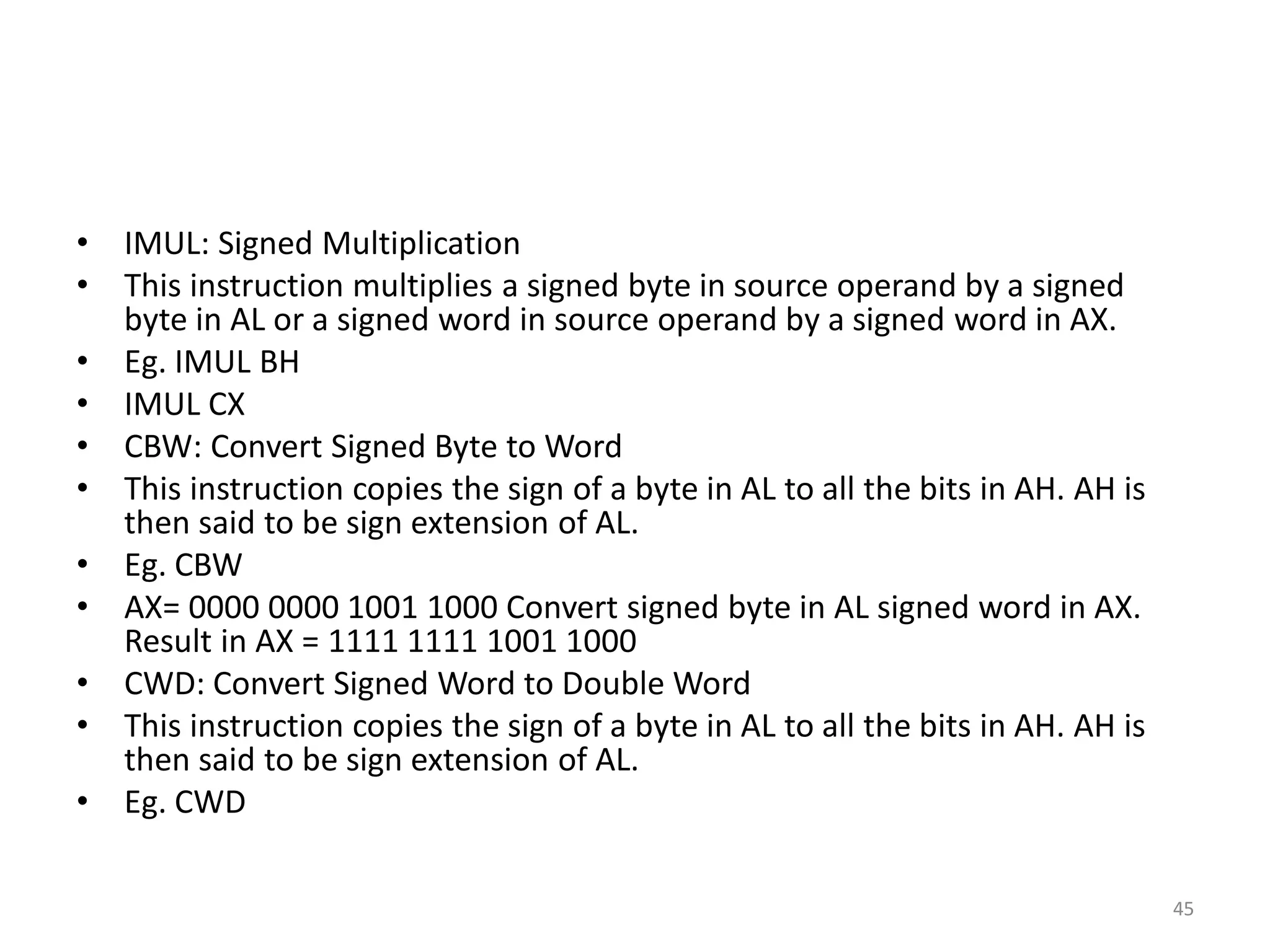
• MUL:Unsigned Multiplication Byte or Word
• This instruction multiplies an unsigned byte or word by
the contents of AL.
• Eg. MUL BH; (AX)= (AL) x (BH)
• MUL CX; (DX)(AX) =(AX) x (CX) 44](https://image.slidesharecdn.com/chapter1merged-230928115840-bb6e9c62/75/MP_MC-pdf-44-2048.jpg)
![• DIV: Unsigned division
• This instruction is used to divide an unsigned word by a byte or to
divide an unsigned double word by a word.
• Eg. DIV CL; Word in AX / byte in CL; Quotient in AL, remainder in AH
• DIV CX; Double word in DX and AX / word; in CX, and Quotient in
AX; remainder in DX
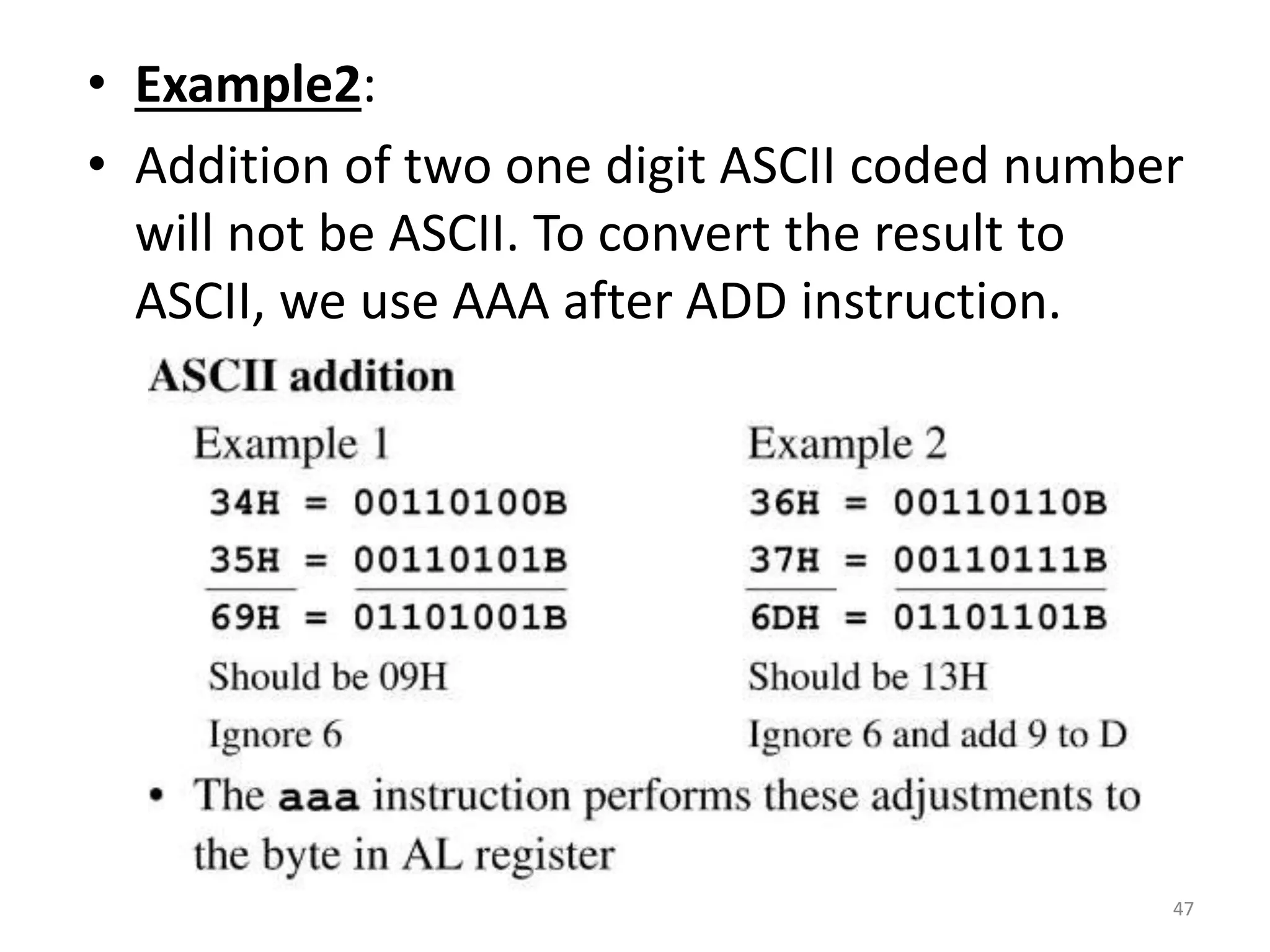
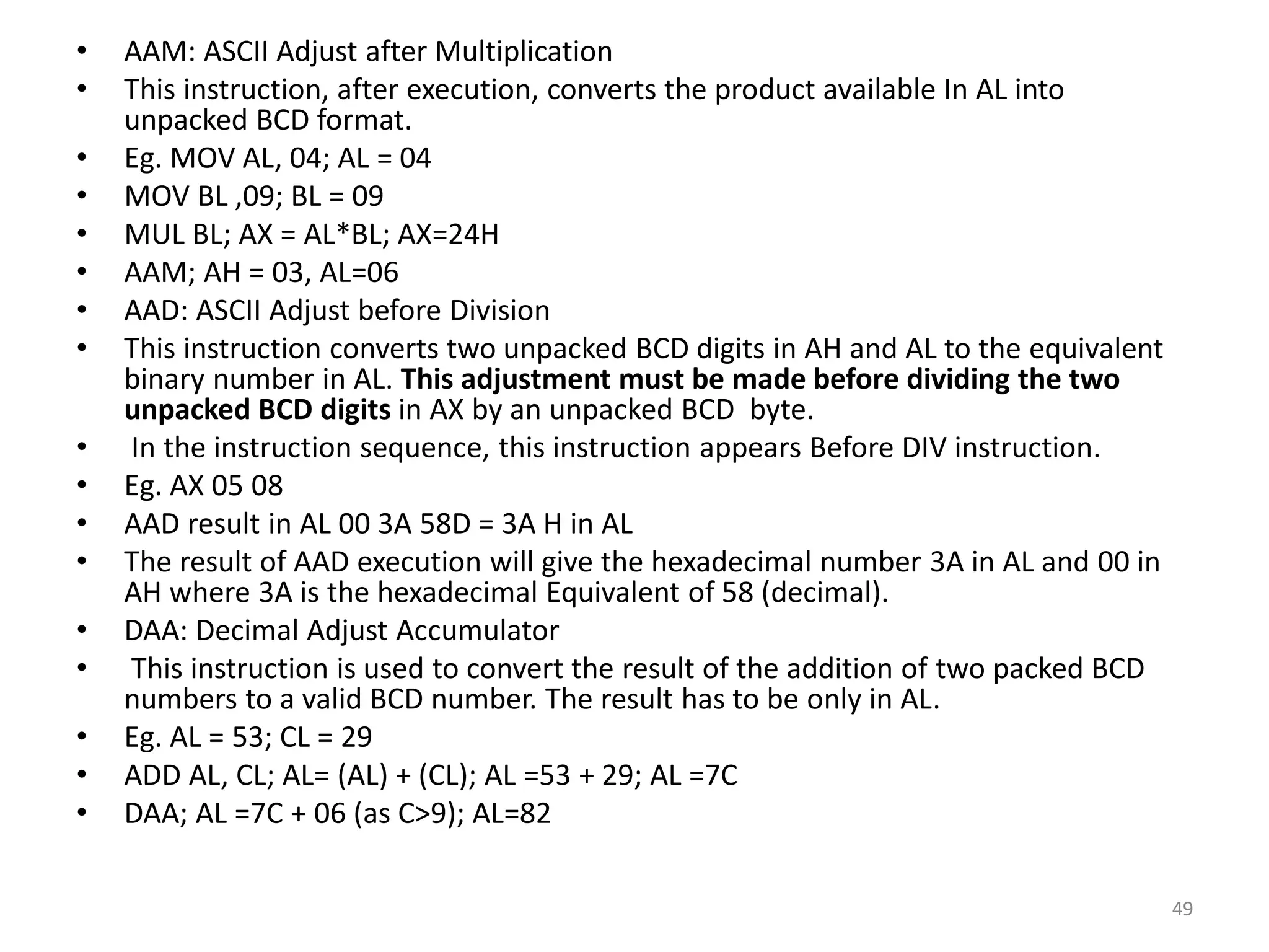
• AAA: ASCII Adjust After Addition
• The AAA instruction is executed after an ADD instruction that adds
two ASCII coded operand to give a byte of result in AL. The AAA
instruction converts the resulting contents of AL to a unpacked
decimal digits.
• Example1: ADD CL, DL; [CL] = 32H = ASCII for 2; [DL] = 35H = ASCII
for 5; Result [CL]= 67H
MOV AL, CL; Move ASCII result into AL since AAA adjust only [AL]
AAA; [AL]=07, unpacked BCD for 7
46](https://image.slidesharecdn.com/chapter1merged-230928115840-bb6e9c62/75/MP_MC-pdf-46-2048.jpg)

![Logical instructions
• Eg. AND AX, 0008H
• AND AX, BX
• OR: Logical OR
• Eg. OR AX, 0008H
• OR AX, BX
• NOT: Logical Invert
• This instruction complements the contents of an operand register or a
memory location, bit by bit.
• Eg. NOT AX
• Eg. XOR AX, 0098H
• XOR AX, BX
• TEST: Logical Compare Instruction
• The TEST instruction performs a bit by bit logical AND operation on the
two operands.
• The result of this ANDing operation is not available for further use, but
flags are affected.
• Eg. TEST AX, BX
• TEST [0500], 06H
51](https://image.slidesharecdn.com/chapter1merged-230928115840-bb6e9c62/75/MP_MC-pdf-51-2048.jpg)


![3 types
• Single register loads & stores
• Multiple register loads & stores
• Single register-memory swap
• All ARM data transfer instructions use register indirect addressing
Single register loads & stores
Examples:
• LDR r0, [r1]; r0=mem[r1]: This instruction will take the address in r1, and
then load a 4 byte value from the memory pointed to by it into register r0
• STR r0, [r1]; mem[r1]=r0
Register indirect with offset:
• LDR r0, [r1, #4]; r0=mem[r1+4]
• STR r0, [r1, #12]; mem[r1+12]=r0
Register indirect with autoindexing:
• LDR r0, [r1, #4]!; r0=mem[r1+4], r1=r1+4
• STR r0, [r1, #12]!; mem[r1+12]=r0, r1=r1+4
Register indirect with postindexing:
• LDR r0, [r1], #4; r0=mem[r1], r1=r1+4
• STR r0, [r1], #12; mem[r1]=r0, r1=r1+12
41
Data Transfer instructions](https://image.slidesharecdn.com/chapter1merged-230928115840-bb6e9c62/75/MP_MC-pdf-282-2048.jpg)
![We can specify a byte or half-word to be transferred
• LDRB r0, [r1]; r0=mem8[r1]
• STRB r0, [r1]; mem8[r1]=r0
• LDRSH r0, [r1]; r0=mem16[r1]; Load signed half word r0 from
memory
• STRSH r0, [r1]; mem16[r1]=r0
Multiple register loads & stores
ARM supports instructions that transfer data between several registers
& memory.
Load Multiple Increment After
• LDMIA r1, (r3,r5,r6); r3=mem[r1], r5=mem[r1+4], r6=mem[r1+8]
Load Multiple Increment Before
• For LDMIB, the addresses will be r1+4, r1+8 and r1+12
• LDMIB r1, (r3,r5,r6); r3=mem[r1+4], r5=mem[r1+8],
r6=mem[r1+12]
42](https://image.slidesharecdn.com/chapter1merged-230928115840-bb6e9c62/75/MP_MC-pdf-283-2048.jpg)


![Microprocessor-Architecture [8085]](https://cdn.slidesharecdn.com/ss_thumbnails/archnakushwaha-171124060226-thumbnail.jpg?width=640&height=640&fit=bounds)


![ANPARA THERMAL POWER STATION[1] sangam.pdf](https://cdn.slidesharecdn.com/ss_thumbnails/anparathermalpowerstation1sangam-251121115219-9261cde4-thumbnail.jpg?width=640&height=640&fit=bounds)


