Download to read offline
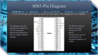


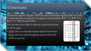

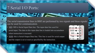


The document discusses the pin configuration of the 8085 microprocessor. It begins by providing a basic pin diagram of the 8085 and stating it can address 64KB of memory and operate at up to 3MHz. It then classifies the 40 pins into 7 groups: 1) Address and Data Bus, 2) Control and Status Signals, 3) Power Supply and Clock Frequency, 4) Interrupts, 5) Reset Signals, 6) External/Peripheral Signals, 7) Serial I/O ports. Each group is then described in 1-2 sentences. The document concludes with a thank you.