The document provides historical context and technical details about microprocessors:
- Ted Hoff at Intel pioneered the concept of the microprocessor in the early 1970s with the Intel 4004, the first commercial microprocessor containing 2,300 transistors.
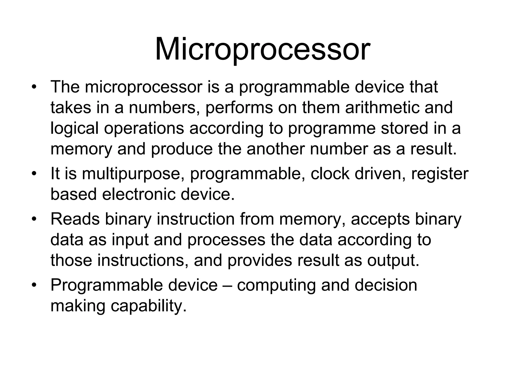
- The microprocessor is a programmable device that takes in data, performs arithmetic and logical operations according to instructions stored in memory, and outputs results. It reads binary instructions from memory to process data.
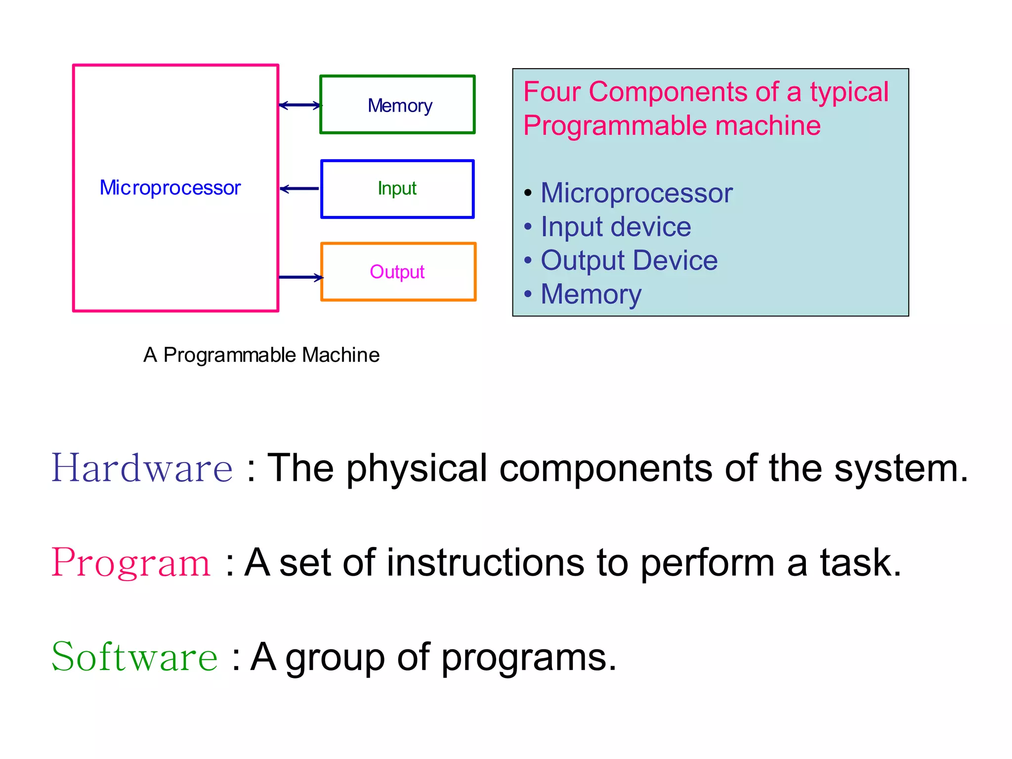
- The typical components of a programmable machine using a microprocessor are the microprocessor itself, input and output devices, and memory to store instructions and data. The microprocessor acts as the central processing unit (CPU) and communicates with memory and I
Historical Perspective
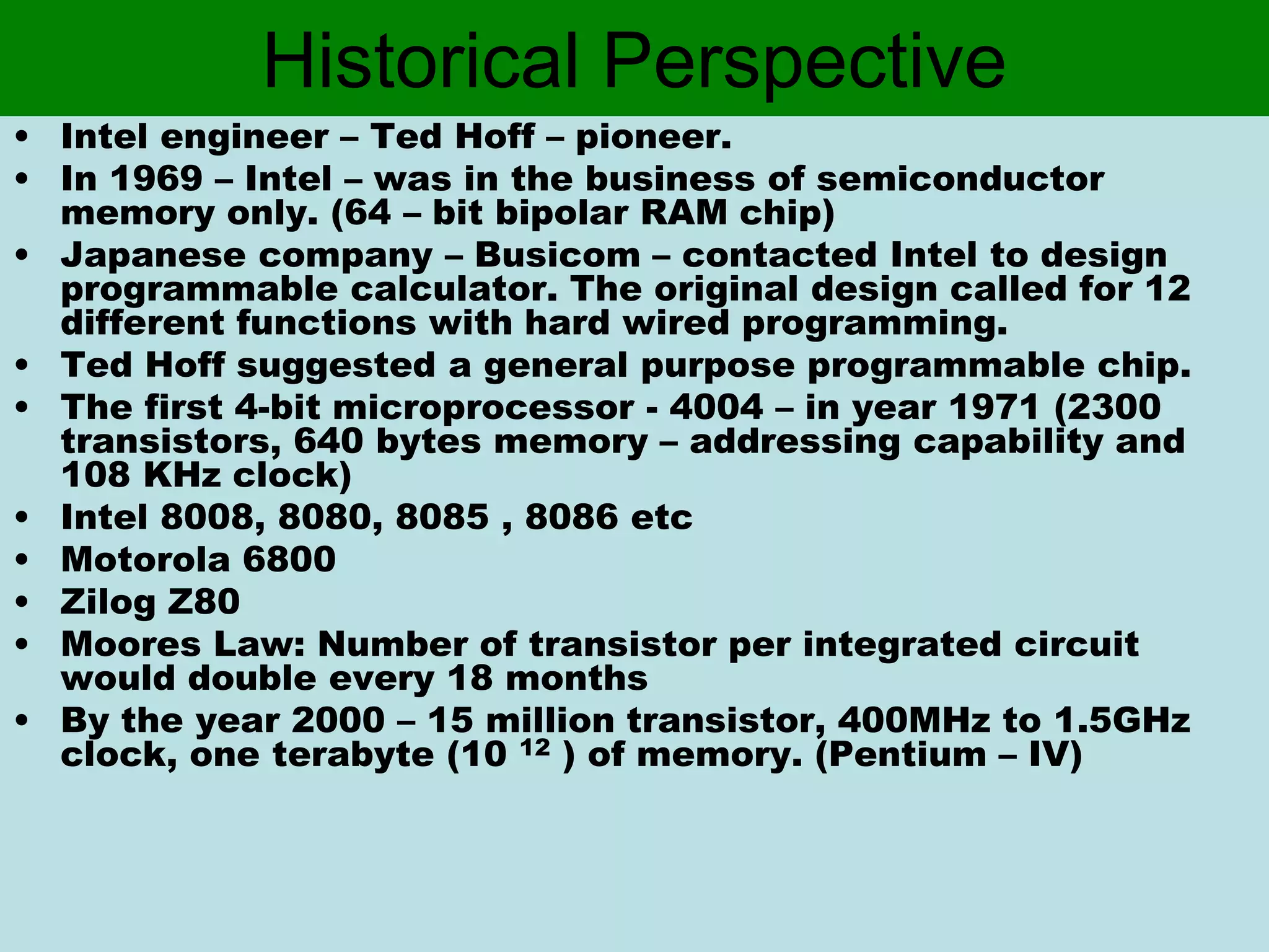
• Intelengineer – Ted Hoff – pioneer.
• In 1969 – Intel – was in the business of semiconductor
memory only. (64 – bit bipolar RAM chip)
• Japanese company – Busicom – contacted Intel to design
programmable calculator. The original design called for 12
different functions with hard wired programming.
• Ted Hoff suggested a general purpose programmable chip.
• The first 4-bit microprocessor - 4004 – in year 1971 (2300
transistors, 640 bytes memory – addressing capability and
108 KHz clock)
• Intel 8008, 8080, 8085 , 8086 etc
• Motorola 6800
• Zilog Z80
• Moores Law: Number of transistor per integrated circuit
would double every 18 months
• By the year 2000 – 15 million transistor, 400MHz to 1.5GHz
clock, one terabyte (10 12 ) of memory. (Pentium – IV)
3.
Microprocessor
• The microprocessoris a programmable device that
takes in a numbers, performs on them arithmetic and
logical operations according to programme stored in a
memory and produce the another number as a result.
• It is multipurpose, programmable, clock driven, register
based electronic device.
• Reads binary instruction from memory, accepts binary
data as input and processes the data according to
those instructions, and provides result as output.
• Programmable device – computing and decision
making capability.
4.
Memory
Input
Output
Microprocessor
A Programmable Machine
Hardware: The physical components of the system.
Program : A set of instructions to perform a task.
Software : A group of programs.
Four Components of a typical
Programmable machine
• Microprocessor
• Input device
• Output Device
• Memory
5.
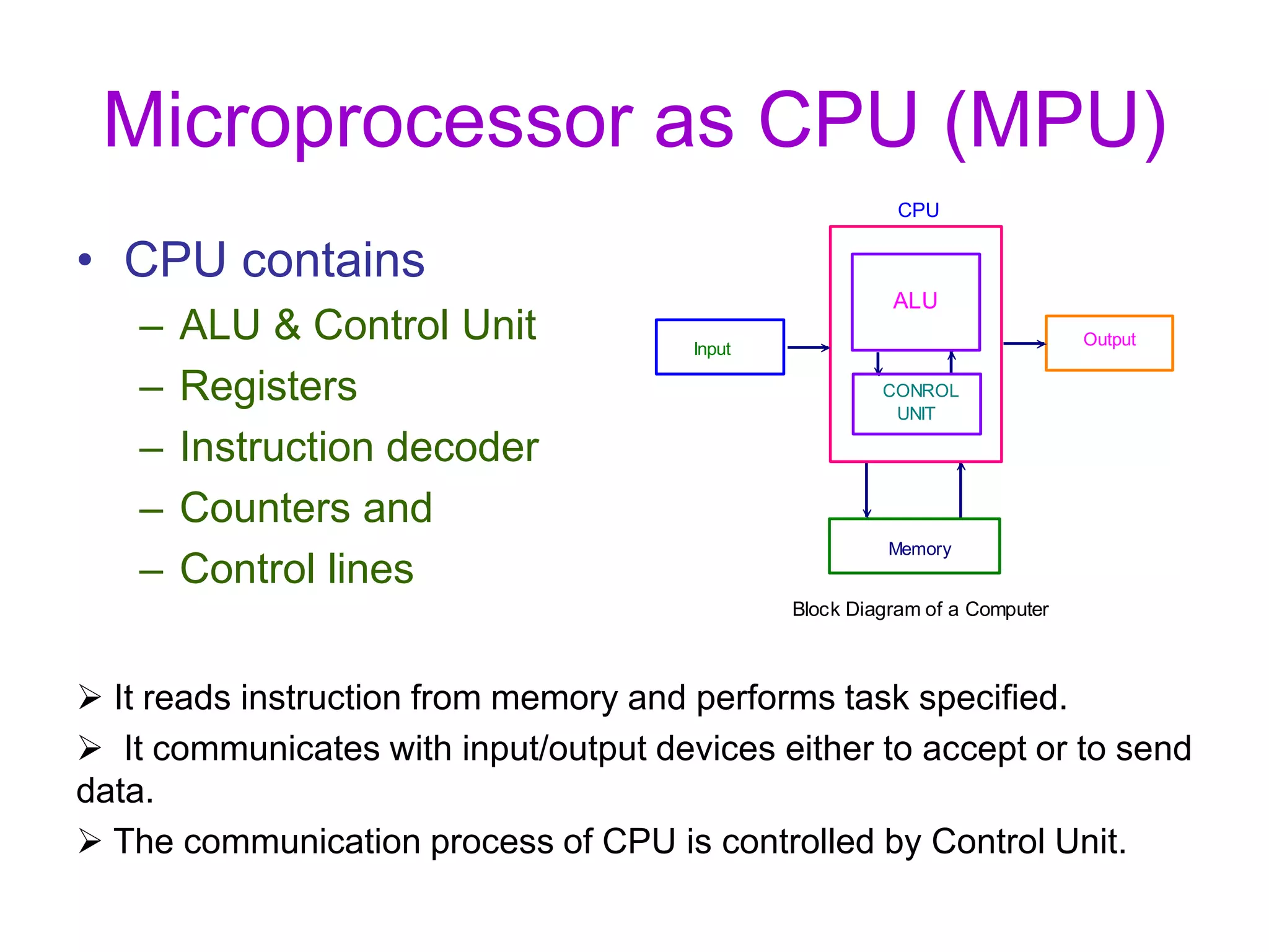
Microprocessor as CPU(MPU)
Memory
Input
Output
CPU
Block Diagram of a Computer
ALU
CONROL
UNIT
• CPU contains
– ALU & Control Unit
– Registers
– Instruction decoder
– Counters and
– Control lines
It reads instruction from memory and performs task specified.
It communicates with input/output devices either to accept or to send
data.
The communication process of CPU is controlled by Control Unit.
6.
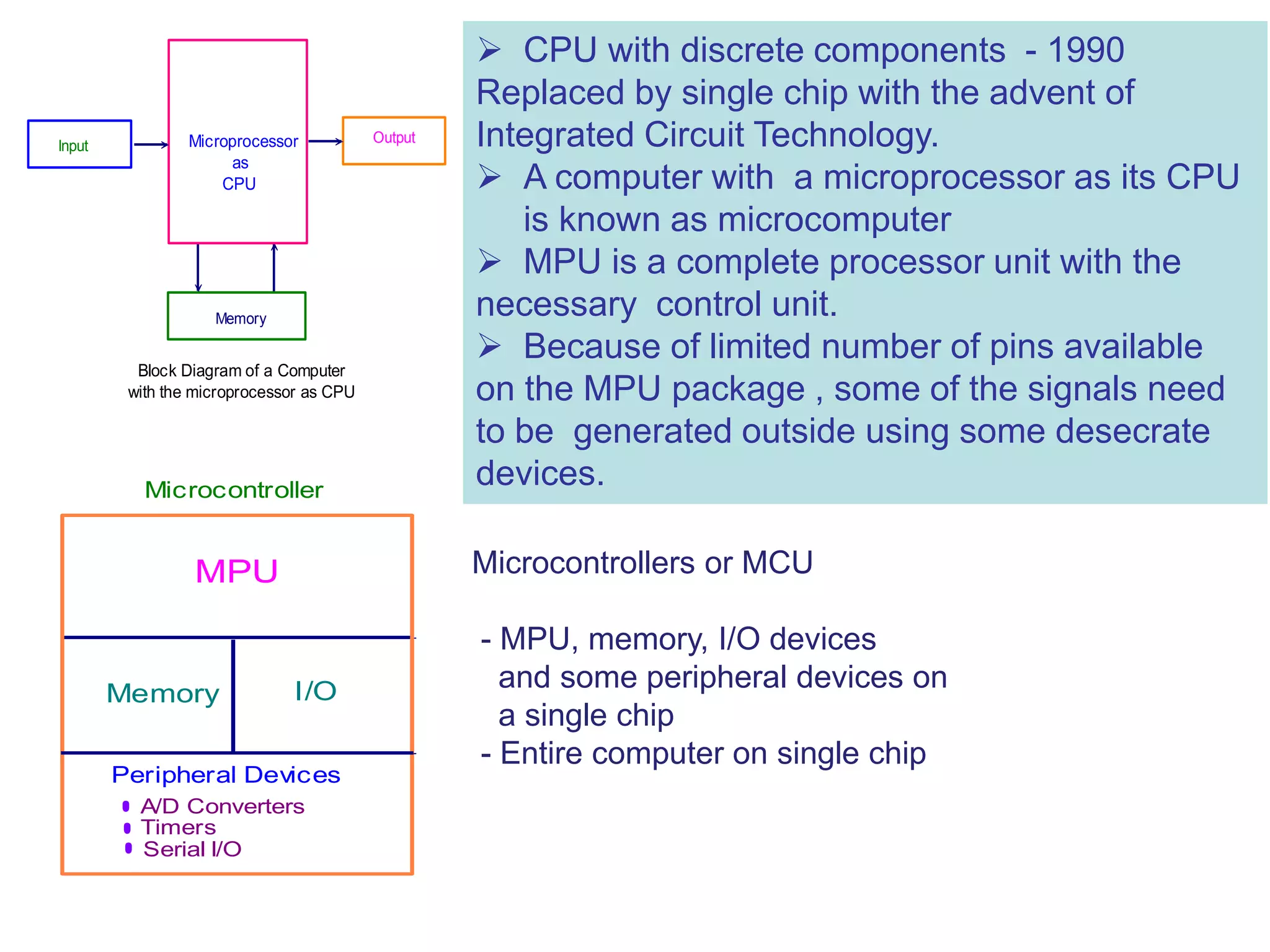
Memory
Input
Output
Microprocessor
as
CPU
Block Diagram ofa Computer
with the microprocessor as CPU
CPU with discrete components - 1990
Replaced by single chip with the advent of
Integrated Circuit Technology.
A computer with a microprocessor as its CPU
is known as microcomputer
MPU is a complete processor unit with the
necessary control unit.
Because of limited number of pins available
on the MPU package , some of the signals need
to be generated outside using some desecrate
devices.
MPU
Memory I/O
Peripheral Devices
A/D Converters
Timers
Serial I/O
Microcontroller
Microcontrollers or MCU
- MPU, memory, I/O devices
and some peripheral devices on
a single chip
- Entire computer on single chip
7.
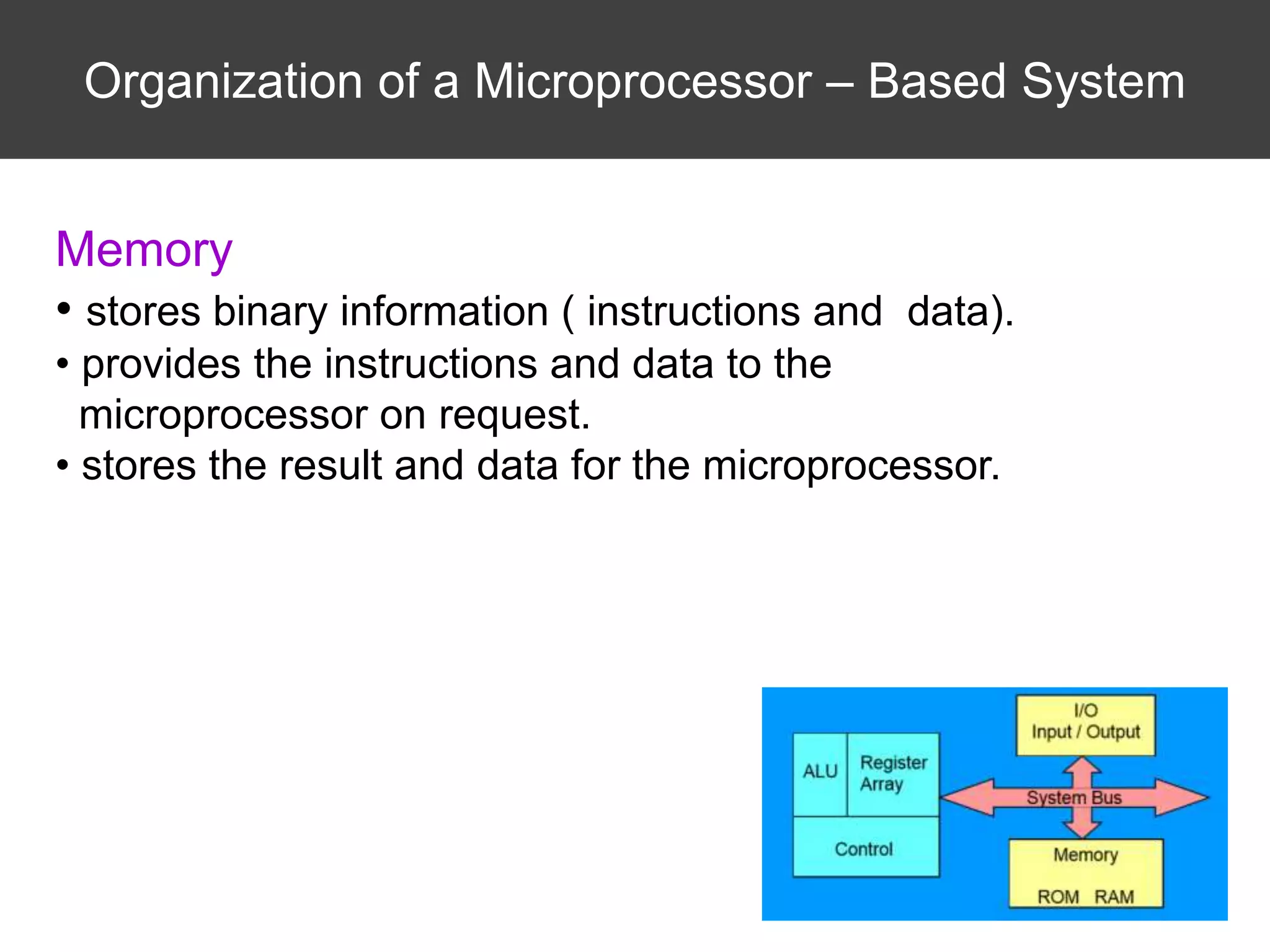
Organization of aMicroprocessor – Based System
Mcroprocessor
ALU Register
Array
Control Unit
I/O
Input / Output
Memory
ROM R / WM
System Bus
Microprocessor
reads instructions from memory.
communicates with all peripherals using system bus.
controls timing of information flow.
performs the computing task specified in a program.
Memory
• stores binary information ( instructions and data).
• provides the instructions and data to the
microprocessor on request.
• stores the result and data for the microprocessor.
8.
Arithmetic/Logic Unit:The ALU unit performs arithmetic operations such as
addition and subtraction, and logic operations such as AND, OR, and exclusive
OR.
Register Array: This area of the microprocessor consists of various registers
identified by letters such as B, C, D, E, H, and L. These registers are primarily
used to store data temporarily during the execution of a program and are
accessible to the user through instructions.
Control Unit: The control unit provides the necessary timing and control signals
to all the operations in the microcomputer. It controls the flow of data between
the microprocessor and memory and peripherals.
Memory: Memory stores binary information such as instructions and data, and
provides that information to the microprocessor whenever necessary. To execute
programs, the microprocessor reads instructions and data from memory and
performs the computing operations in its ALU section. Results are either
transferred to the output section for display or stored in memory for later use.
Read-Only memory (ROM) and Read/Write memory (R/WM), popularly known
as Random- Access memory (RAM).
9.
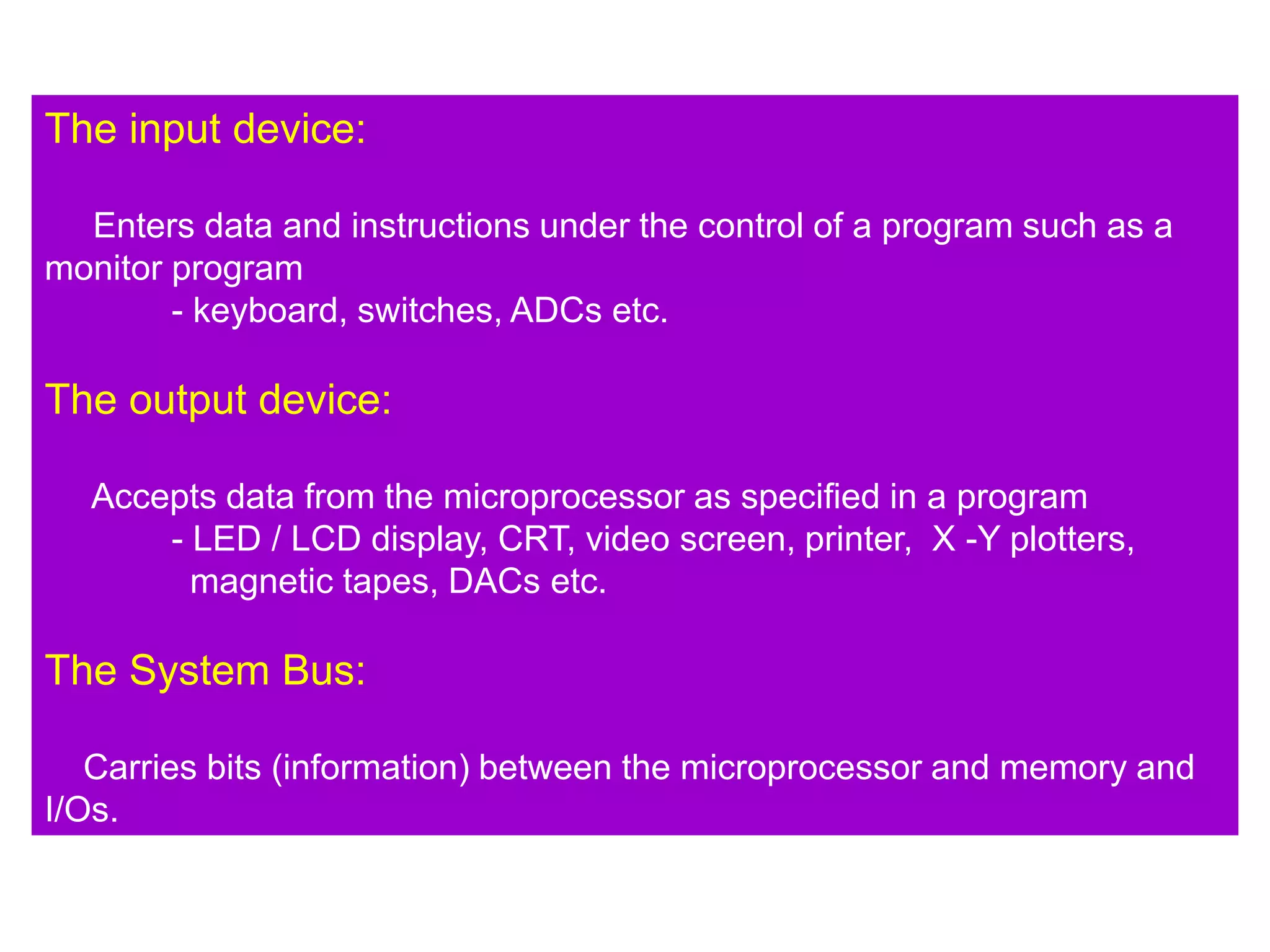
The input device:
Entersdata and instructions under the control of a program such as a
monitor program
- keyboard, switches, ADCs etc.
The output device:
Accepts data from the microprocessor as specified in a program
- LED / LCD display, CRT, video screen, printer, X -Y plotters,
magnetic tapes, DACs etc.
The System Bus:
Carries bits (information) between the microprocessor and memory and
I/Os.
10.
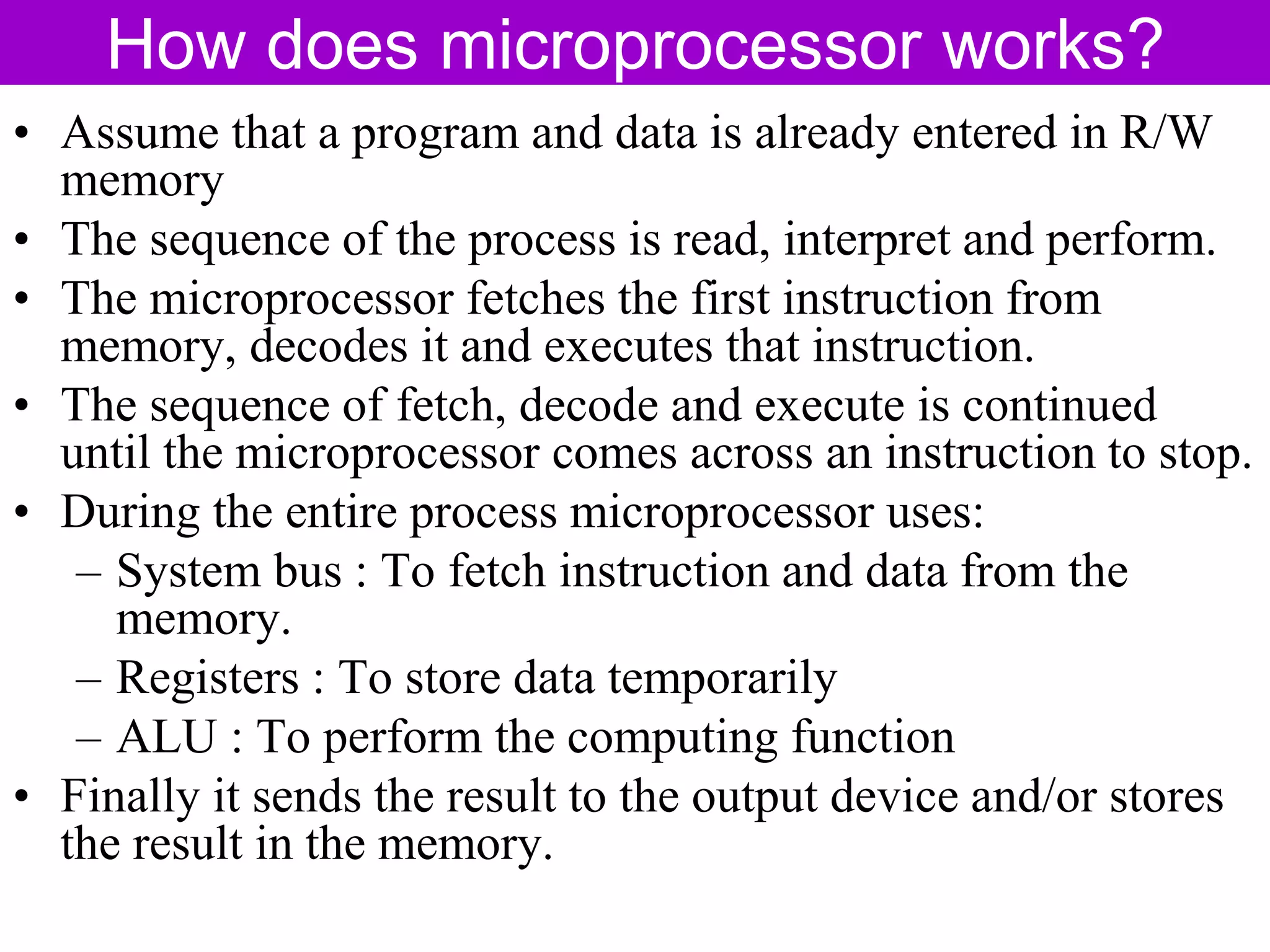
How does microprocessorworks?
• Assume that a program and data is already entered in R/W
memory
• The sequence of the process is read, interpret and perform.
• The microprocessor fetches the first instruction from
memory, decodes it and executes that instruction.
• The sequence of fetch, decode and execute is continued
until the microprocessor comes across an instruction to stop.
• During the entire process microprocessor uses:
– System bus : To fetch instruction and data from the
memory.
– Registers : To store data temporarily
– ALU : To perform the computing function
• Finally it sends the result to the output device and/or stores
the result in the memory.
11.
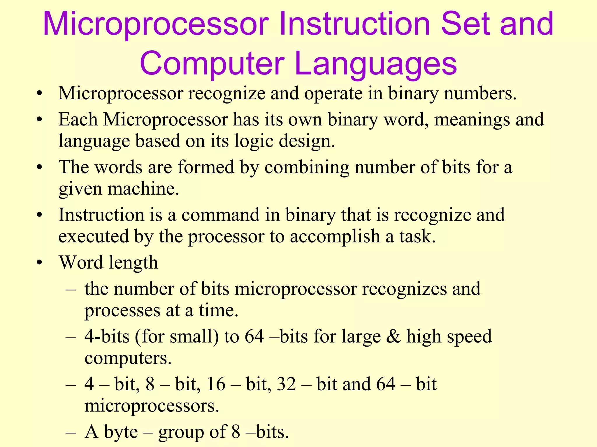
Microprocessor Instruction Setand
Computer Languages
• Microprocessor recognize and operate in binary numbers.
• Each Microprocessor has its own binary word, meanings and
language based on its logic design.
• The words are formed by combining number of bits for a
given machine.
• Instruction is a command in binary that is recognize and
executed by the processor to accomplish a task.
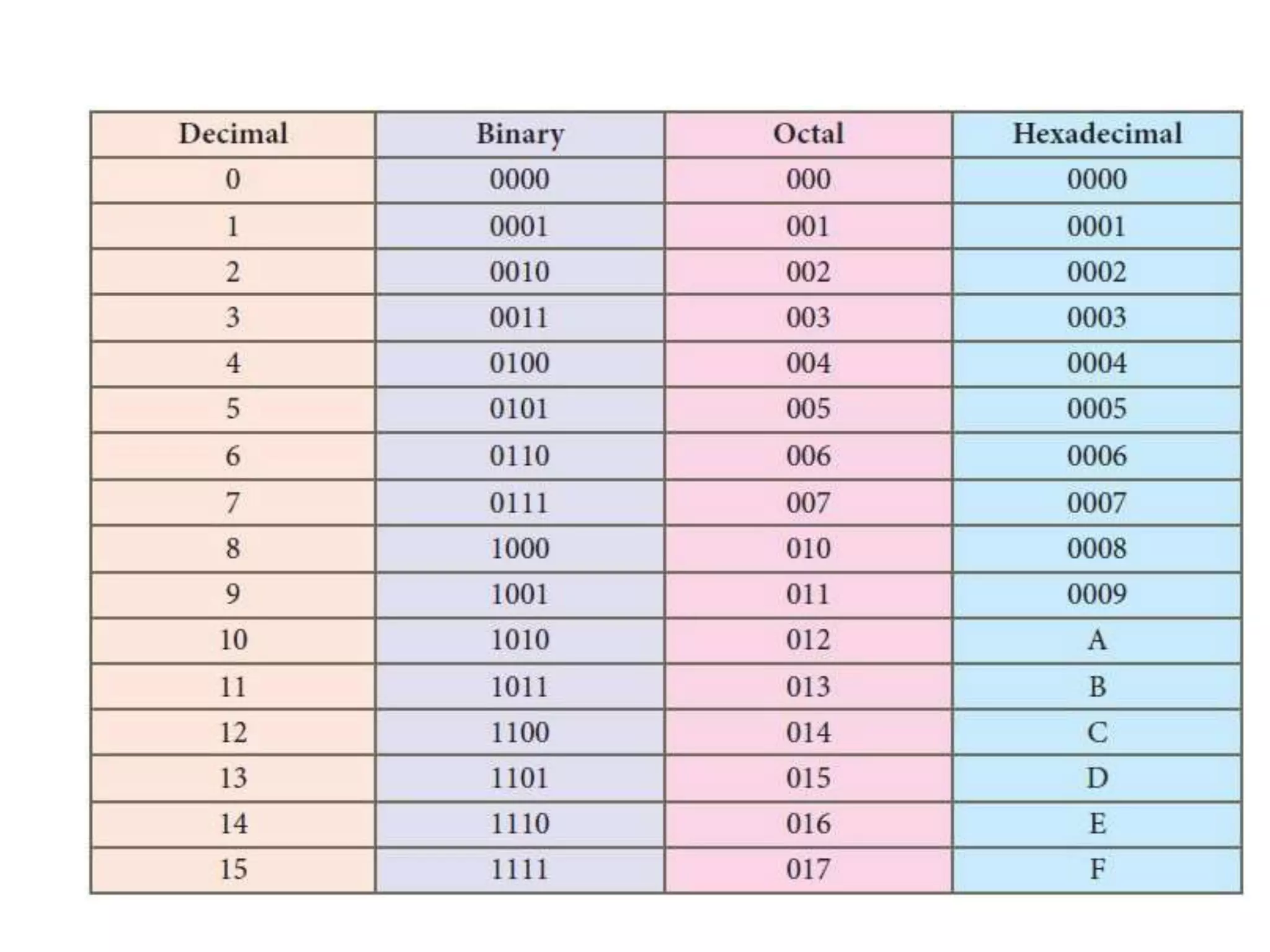
• Word length
– the number of bits microprocessor recognizes and
processes at a time.
– 4-bits (for small) to 64 –bits for large & high speed
computers.
– 4 – bit, 8 – bit, 16 – bit, 32 – bit and 64 – bit
microprocessors.
– A byte – group of 8 –bits.
12.
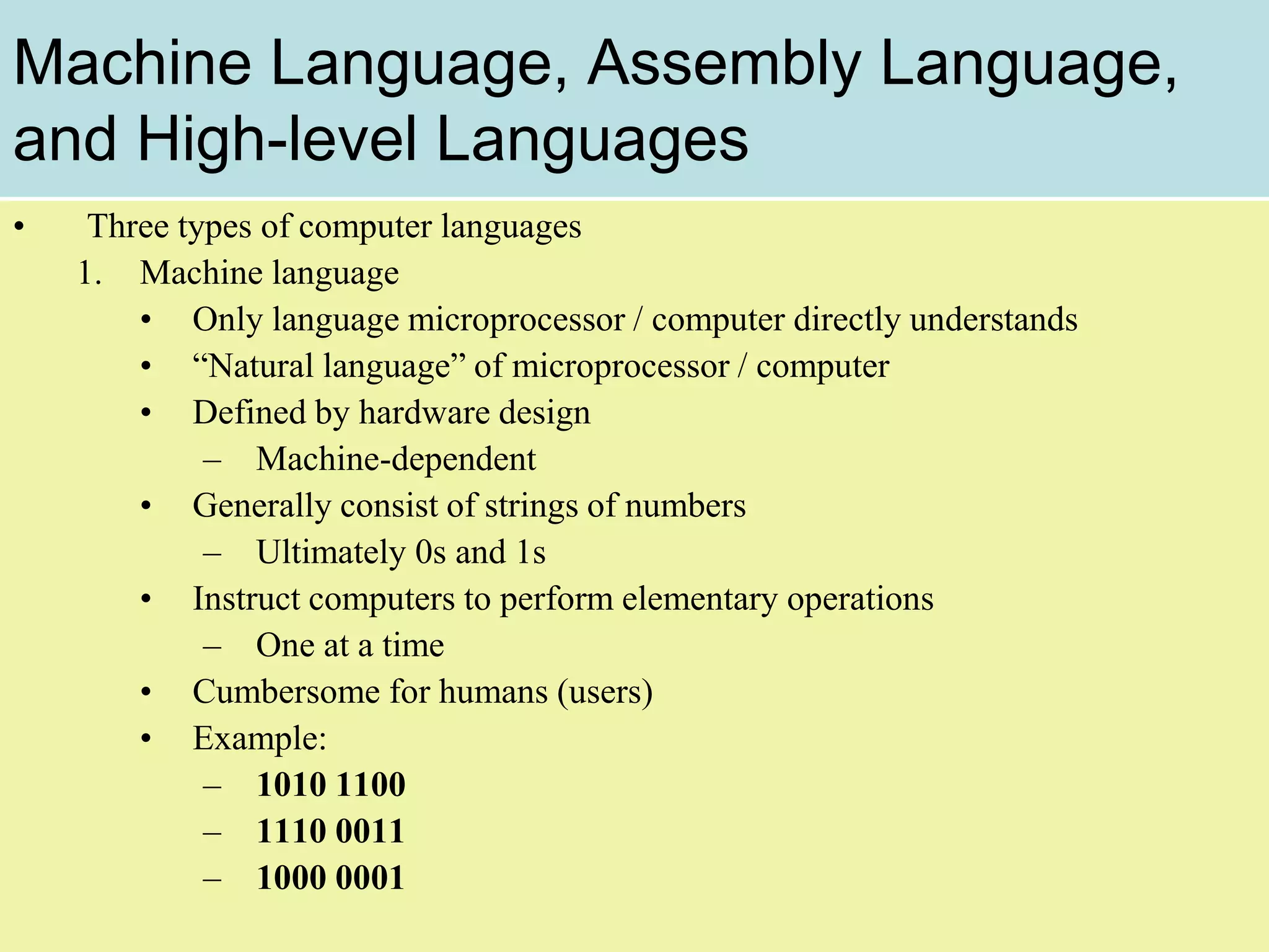
Machine Language, AssemblyLanguage,
and High-level Languages
• Three types of computer languages
1. Machine language
• Only language microprocessor / computer directly understands
• “Natural language” of microprocessor / computer
• Defined by hardware design
– Machine-dependent
• Generally consist of strings of numbers
– Ultimately 0s and 1s
• Instruct computers to perform elementary operations
– One at a time
• Cumbersome for humans (users)
• Example:
– 1010 1100
– 1110 0011
– 1000 0001
13.
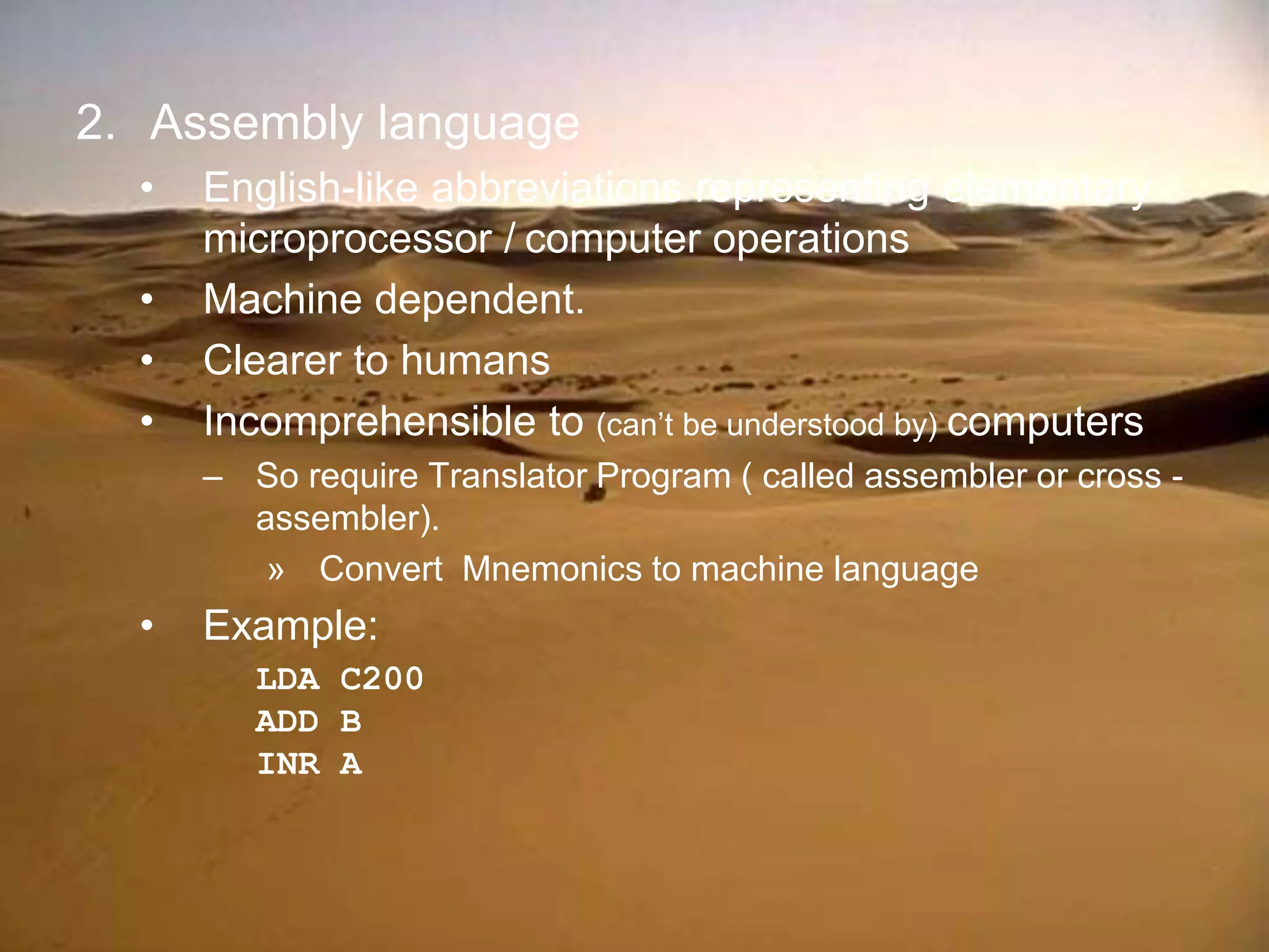
2. Assembly language
•English-like abbreviations representing elementary
microprocessor / computer operations
• Machine dependent.
• Clearer to humans
• Incomprehensible to (can’t be understood by) computers
– So require Translator Program ( called assembler or cross -
assembler).
» Convert Mnemonics to machine language
• Example:
LDA C200
ADD B
INR A
14.
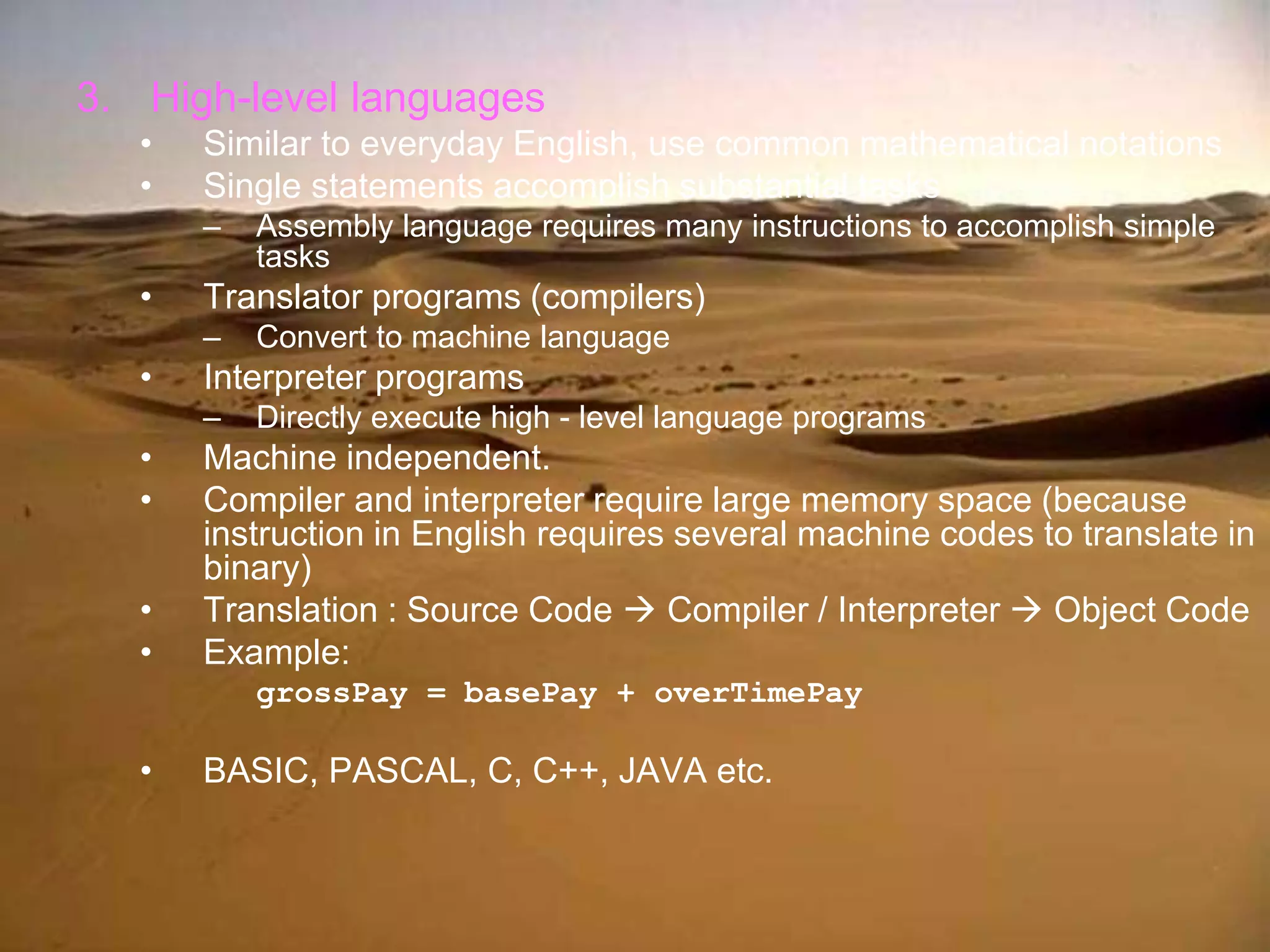
3. High-level languages
•Similar to everyday English, use common mathematical notations
• Single statements accomplish substantial tasks
– Assembly language requires many instructions to accomplish simple
tasks
• Translator programs (compilers)
– Convert to machine language
• Interpreter programs
– Directly execute high - level language programs
• Machine independent.
• Compiler and interpreter require large memory space (because
instruction in English requires several machine codes to translate in
binary)
• Translation : Source Code Compiler / Interpreter Object Code
• Example:
grossPay = basePay + overTimePay
• BASIC, PASCAL, C, C++, JAVA etc.
15.
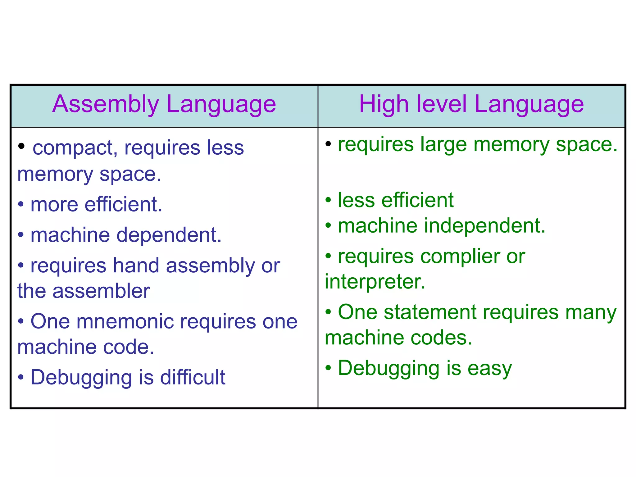
Assembly Language Highlevel Language
• compact, requires less
memory space.
• more efficient.
• machine dependent.
• requires hand assembly or
the assembler
• One mnemonic requires one
machine code.
• Debugging is difficult
• requires large memory space.
• less efficient
• machine independent.
• requires complier or
interpreter.
• One statement requires many
machine codes.
• Debugging is easy
16.
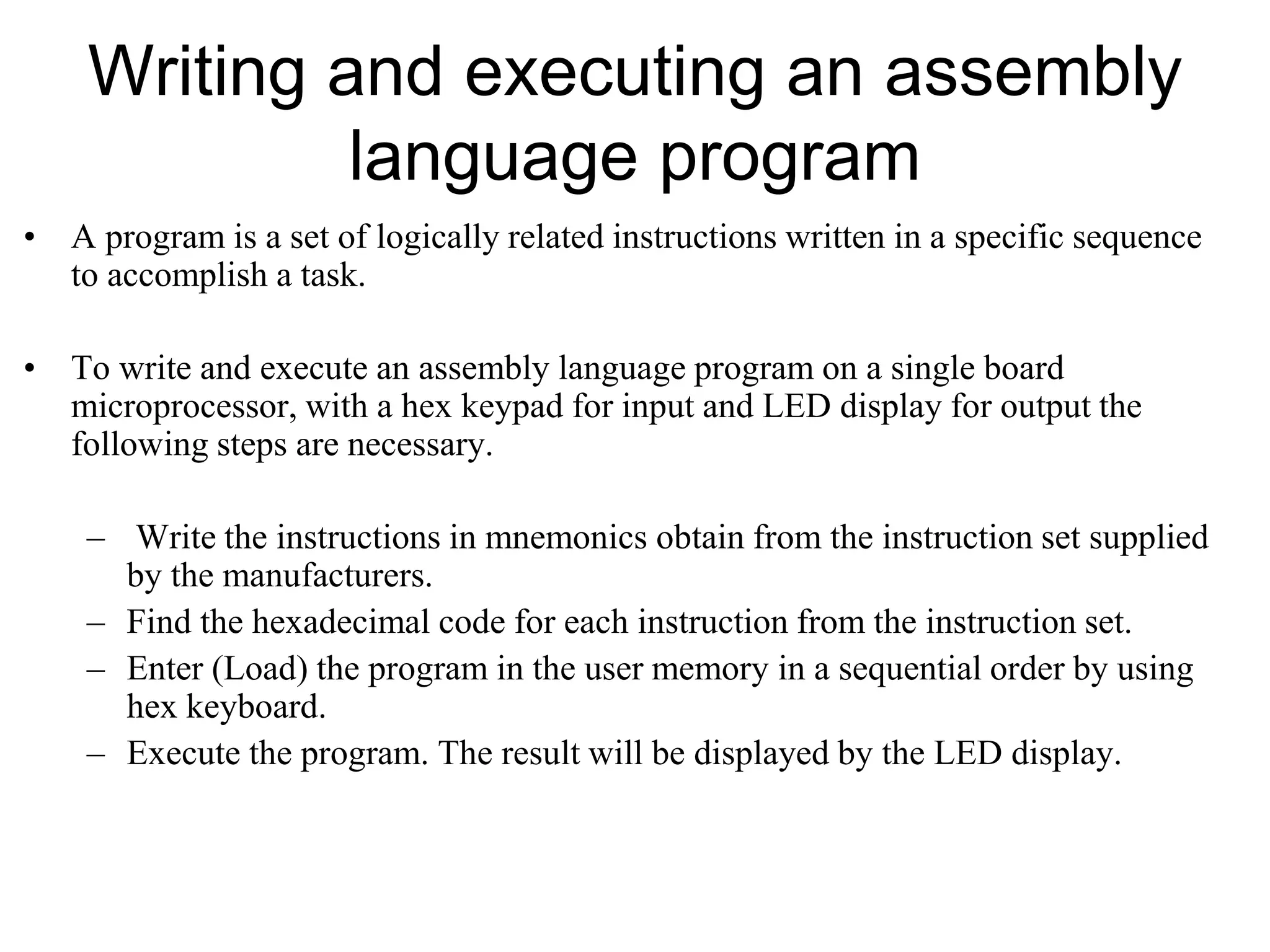
Writing and executingan assembly
language program
• A program is a set of logically related instructions written in a specific sequence
to accomplish a task.
• To write and execute an assembly language program on a single board
microprocessor, with a hex keypad for input and LED display for output the
following steps are necessary.
– Write the instructions in mnemonics obtain from the instruction set supplied
by the manufacturers.
– Find the hexadecimal code for each instruction from the instruction set.
– Enter (Load) the program in the user memory in a sequential order by using
hex keyboard.
– Execute the program. The result will be displayed by the LED display.
17.
Buses
Registers
ALU
Flags
Program Counter(PC)
Stack Pointer(SP)
Instruction registers and decoders
Timing and control circuit
18.
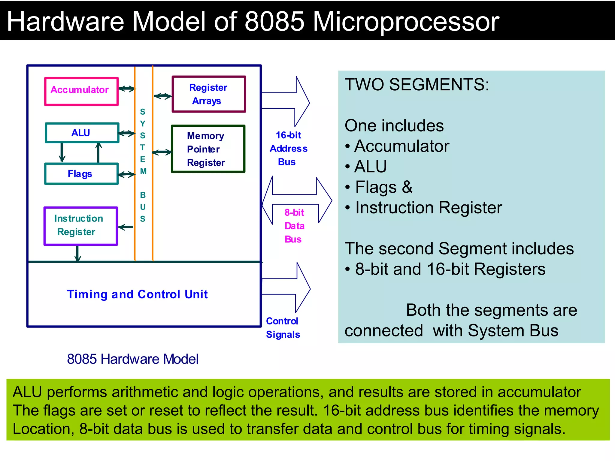
Accumulator
ALU
Flags
Instruction
Register
Register
Arrays
Memory
Pointer
Register
Timing and ControlUnit
16-bit
Address
Bus
8-bit
Data
Bus
Control
Signals
8085 Hardware Model
S
Y
S
T
E
M
B
U
S
TWO SEGMENTS:
One includes
• Accumulator
• ALU
• Flags &
• Instruction Register
The second Segment includes
• 8-bit and 16-bit Registers
Both the segments are
connected with System Bus
ALU performs arithmetic and logic operations, and results are stored in accumulator
The flags are set or reset to reflect the result. 16-bit address bus identifies the memory
Location, 8-bit data bus is used to transfer data and control bus for timing signals.
Hardware Model of 8085 Microprocessor
19.
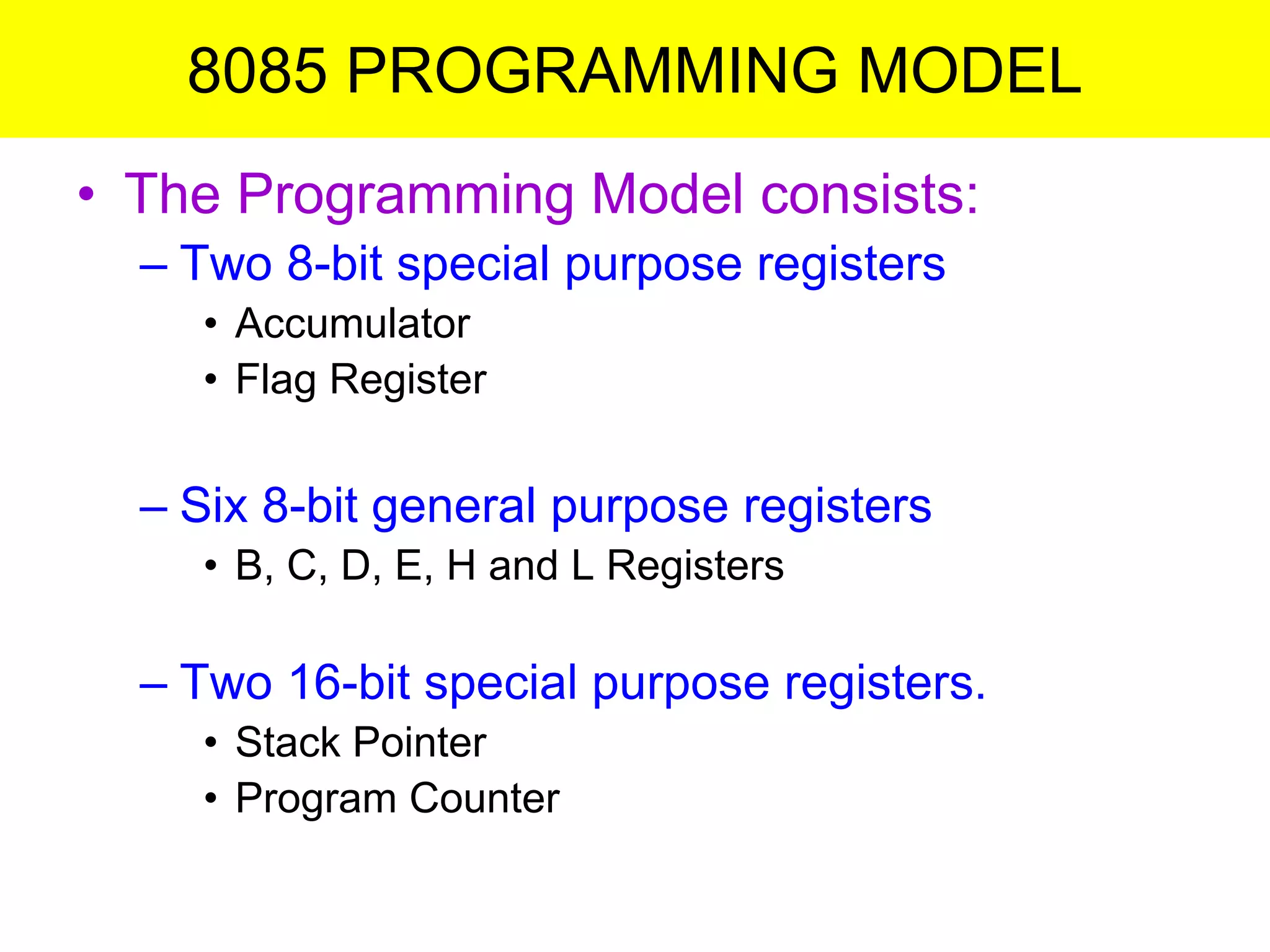
8085 PROGRAMMING MODEL
•The Programming Model consists:
– Two 8-bit special purpose registers
• Accumulator
• Flag Register
– Six 8-bit general purpose registers
• B, C, D, E, H and L Registers
– Two 16-bit special purpose registers.
• Stack Pointer
• Program Counter
20.
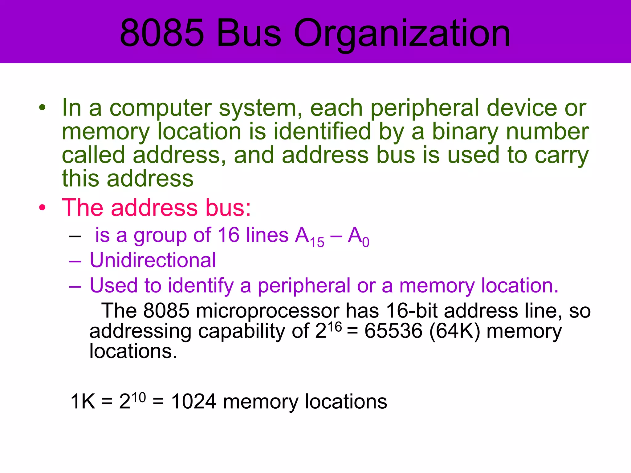
8085 Bus Organization
•In a computer system, each peripheral device or
memory location is identified by a binary number
called address, and address bus is used to carry
this address
• The address bus:
– is a group of 16 lines A15 – A0
– Unidirectional
– Used to identify a peripheral or a memory location.
The 8085 microprocessor has 16-bit address line, so
addressing capability of 216 = 65536 (64K) memory
locations.
1K = 210 = 1024 memory locations
22.
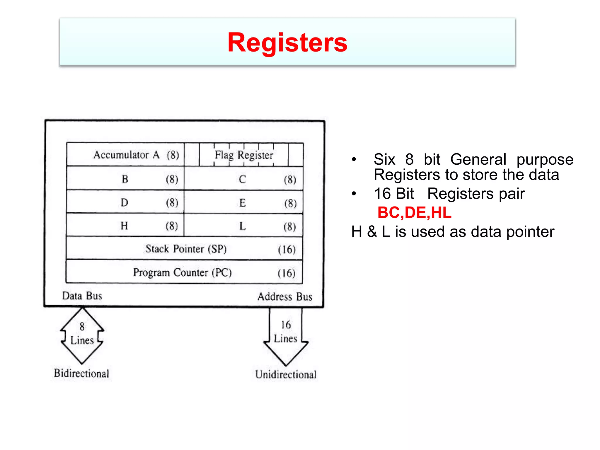
Accumulator A (8)Flag Register (8)
B (8) C (8)
D (8) E (8)
L (8)
H (8)
Stack Pointer (SP) (16)
Program Counter (PC) (16)
Data Bus Address Bus
Bidirectional
Unidirectional
8
Lines
16
Lines
Programming Model of 8085
Register A (Accumulator):
>> It is tri-state 8-bit register
>> After performing arithmetic and logic operations ALU places
result on the internal data bus from there it is generally stored in
accumulator.
>> It is also used in load and store operations,
as well as in input /output (I/O) operations.
>> Most of the times the results of arithmetic and logical operations
is stored in register A, hence it is called as accumulator.
>> The register A can be used as a general-purpose register.
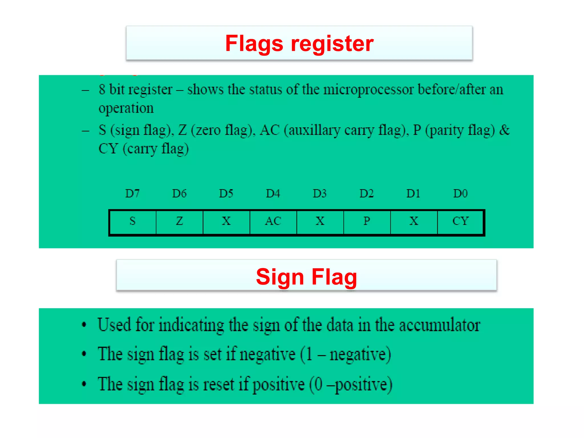
Flag register is a group of five flip-flops used to
give status of the operations performed by ALU
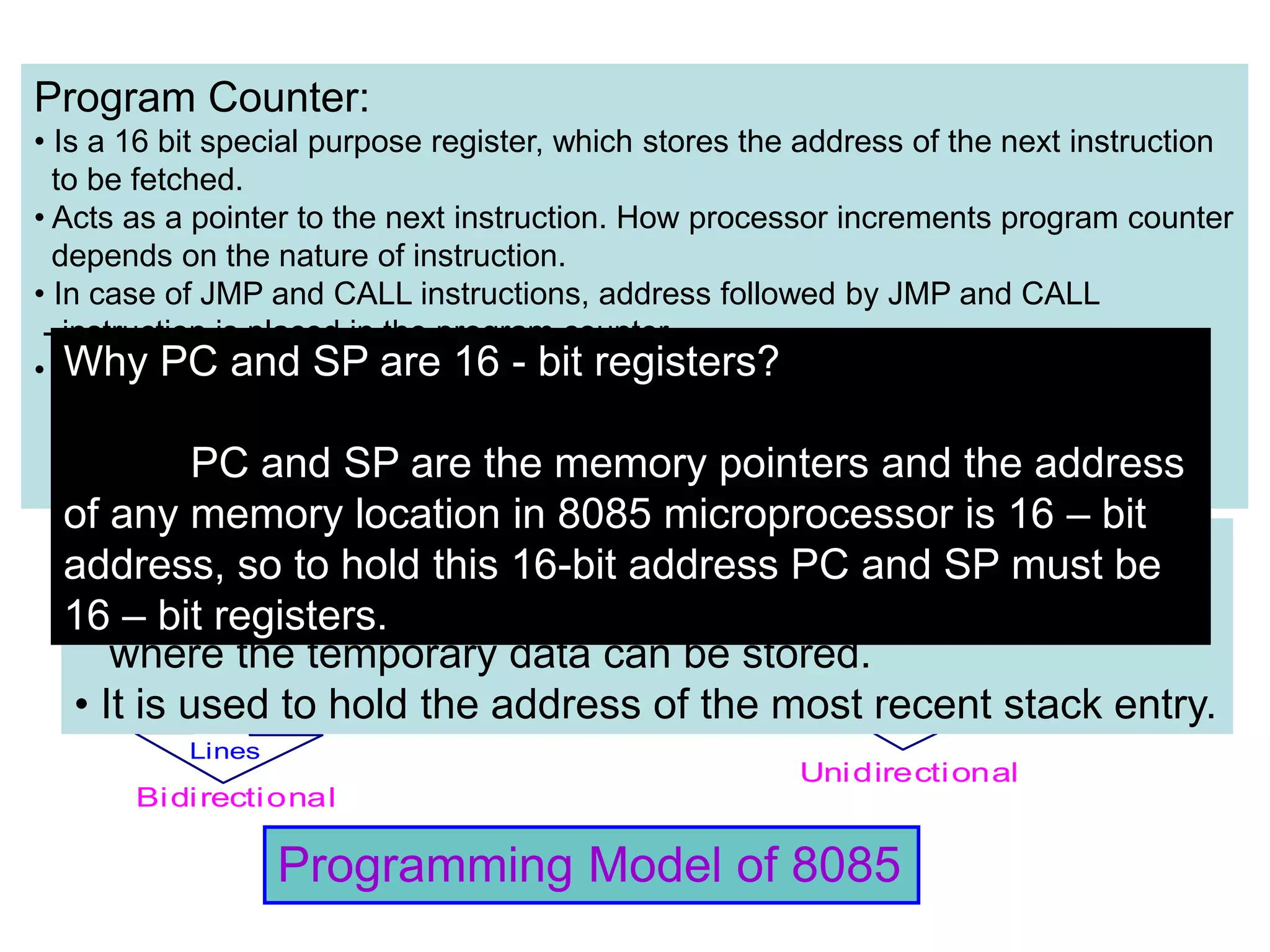
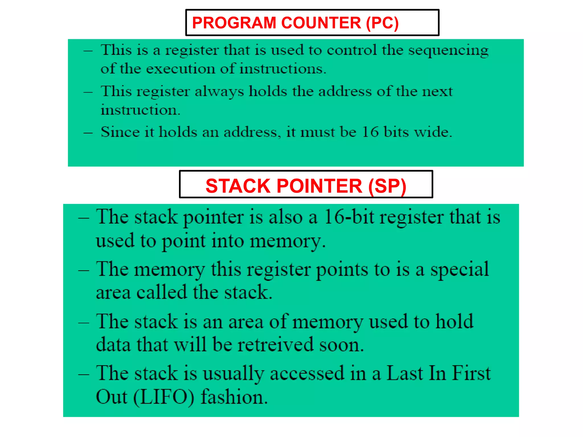
Program Counter:
• Is a 16 bit special purpose register, which stores the address of the next instruction
to be fetched.
• Acts as a pointer to the next instruction. How processor increments program counter
depends on the nature of instruction.
• In case of JMP and CALL instructions, address followed by JMP and CALL
- instruction is placed in the program counter.
• In case of Conditional JMP and Conditional CALL instructions,
address followed by JMP and CALL instructions is placed in the program counter
if the condition is satisfied; otherwise the program counter is incremented by three
so as to point the address of the next instruction to be fetched.
Stack Pointer:
• The stack is the reserved area of the memory in the RAM
where the temporary data can be stored.
• It is used to hold the address of the most recent stack entry.
Why PC and SP are 16 - bit registers?
PC and SP are the memory pointers and the address
of any memory location in 8085 microprocessor is 16 – bit
address, so to hold this 16-bit address PC and SP must be
16 – bit registers.
23.
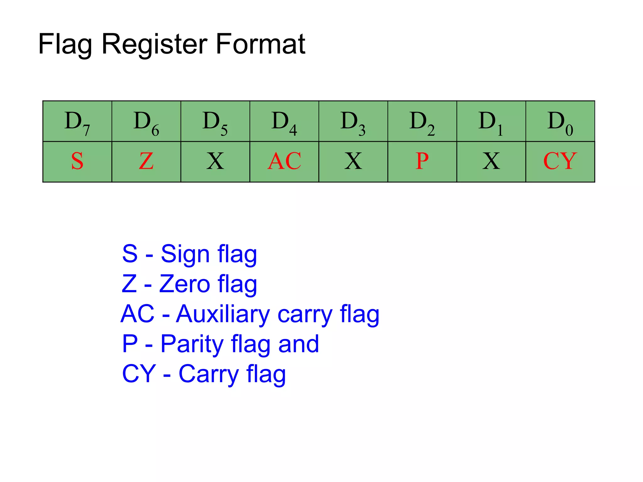
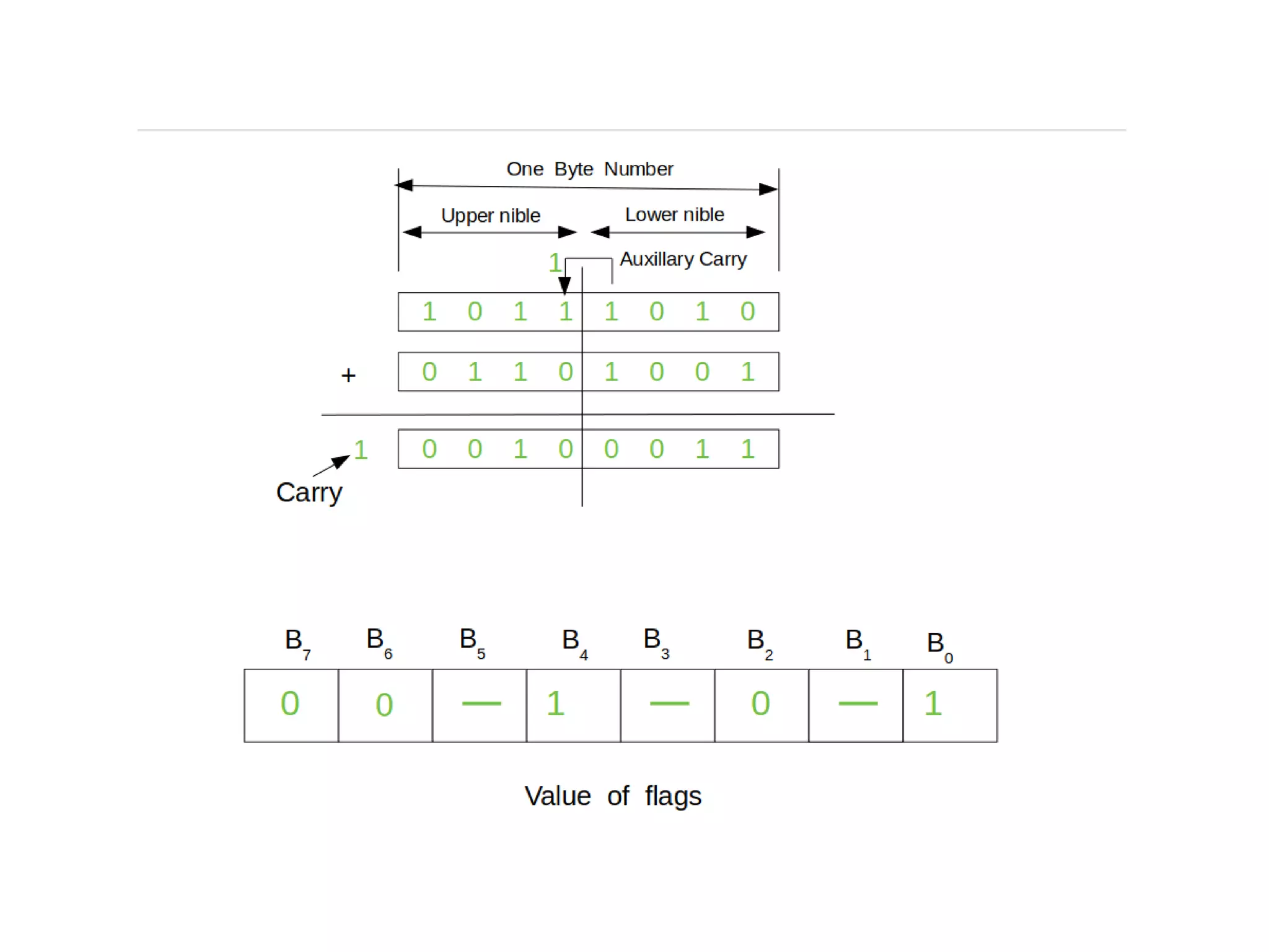
D7 D6 D5D4 D3 D2 D1 D0
S Z X AC X P X CY
Flag Register Format
S - Sign flag
Z - Zero flag
AC - Auxiliary carry flag
P - Parity flag and
CY - Carry flag
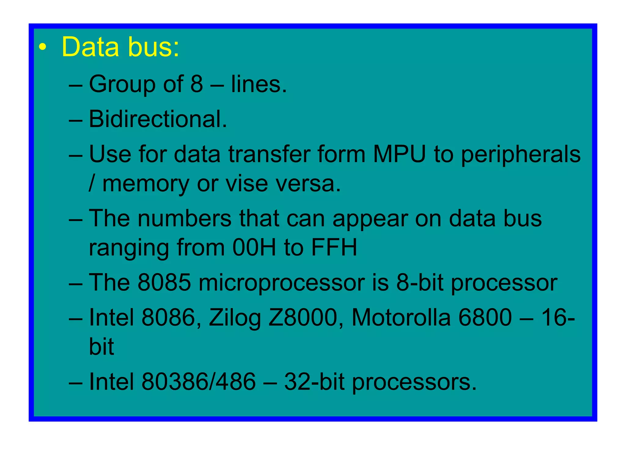
• Data bus:
–Group of 8 – lines.
– Bidirectional.
– Use for data transfer form MPU to peripherals
/ memory or vise versa.
– The numbers that can appear on data bus
ranging from 00H to FFH
– The 8085 microprocessor is 8-bit processor
– Intel 8086, Zilog Z8000, Motorolla 6800 – 16-
bit
– Intel 80386/486 – 32-bit processors.
26.
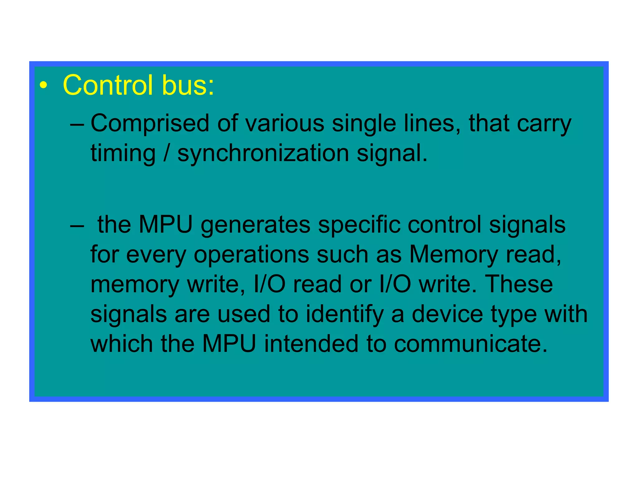
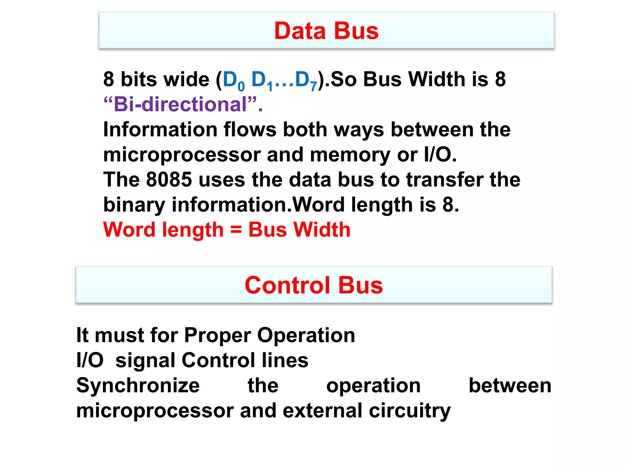
• Control bus:
–Comprised of various single lines, that carry
timing / synchronization signal.
– the MPU generates specific control signals
for every operations such as Memory read,
memory write, I/O read or I/O write. These
signals are used to identify a device type with
which the MPU intended to communicate.
27.
Data Bus
8 bitswide (D0 D1…D7).So Bus Width is 8
“Bi-directional”.
Information flows both ways between the
microprocessor and memory or I/O.
The 8085 uses the data bus to transfer the
binary information.Word length is 8.
Word length = Bus Width
Control Bus
It must for Proper Operation
I/O signal Control lines
Synchronize the operation between
microprocessor and external circuitry
28.
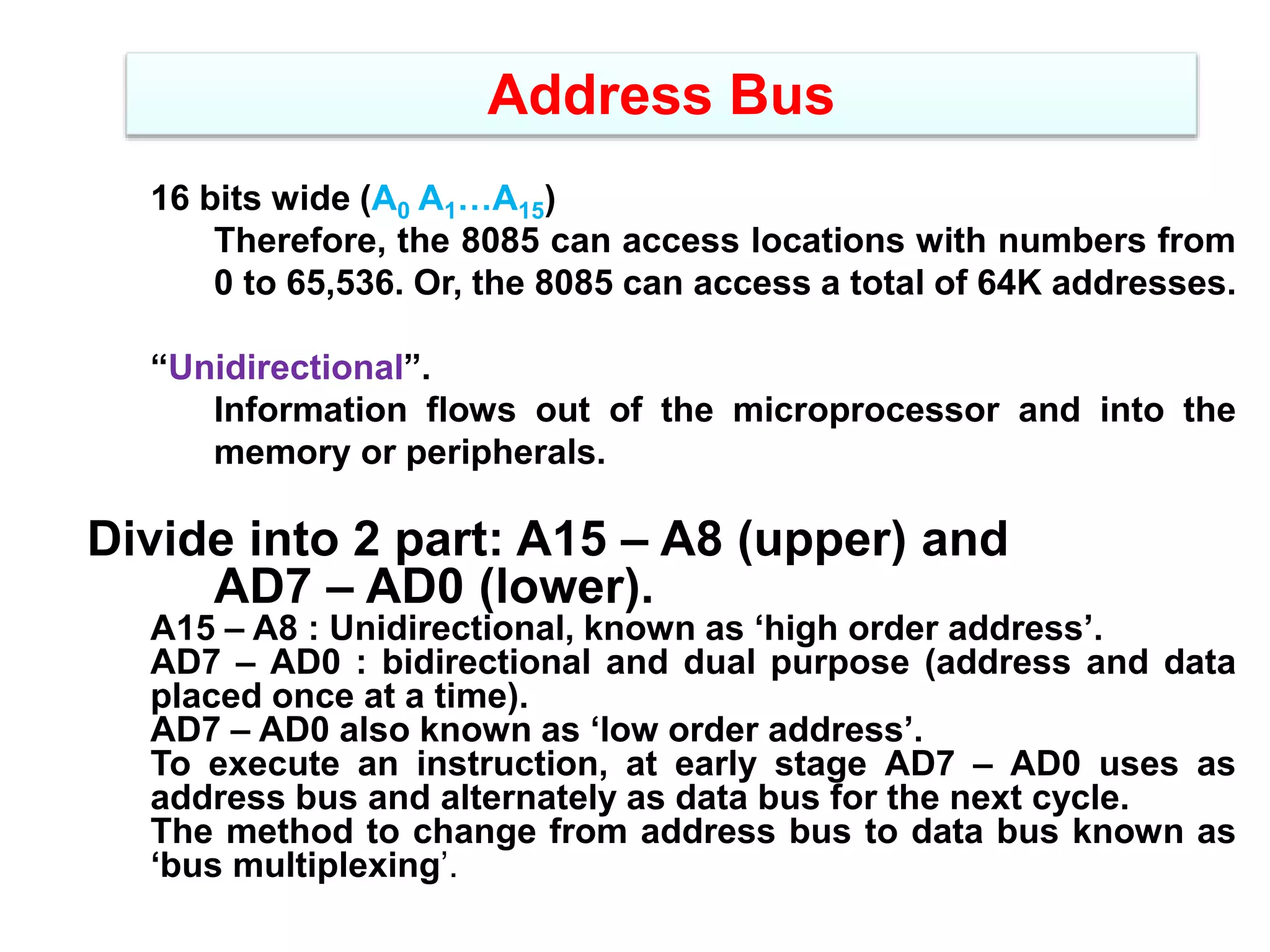
Address Bus
16 bitswide (A0 A1…A15)
Therefore, the 8085 can access locations with numbers from
0 to 65,536. Or, the 8085 can access a total of 64K addresses.
“Unidirectional”.
Information flows out of the microprocessor and into the
memory or peripherals.
Divide into 2 part: A15 – A8 (upper) and
AD7 – AD0 (lower).
A15 – A8 : Unidirectional, known as ‘high order address’.
AD7 – AD0 : bidirectional and dual purpose (address and data
placed once at a time).
AD7 – AD0 also known as ‘low order address’.
To execute an instruction, at early stage AD7 – AD0 uses as
address bus and alternately as data bus for the next cycle.
The method to change from address bus to data bus known as
‘bus multiplexing’.
29.
Registers
• Six 8bit General purpose
Registers to store the data
• 16 Bit Registers pair
BC,DE,HL
H & L is used as data pointer
30.
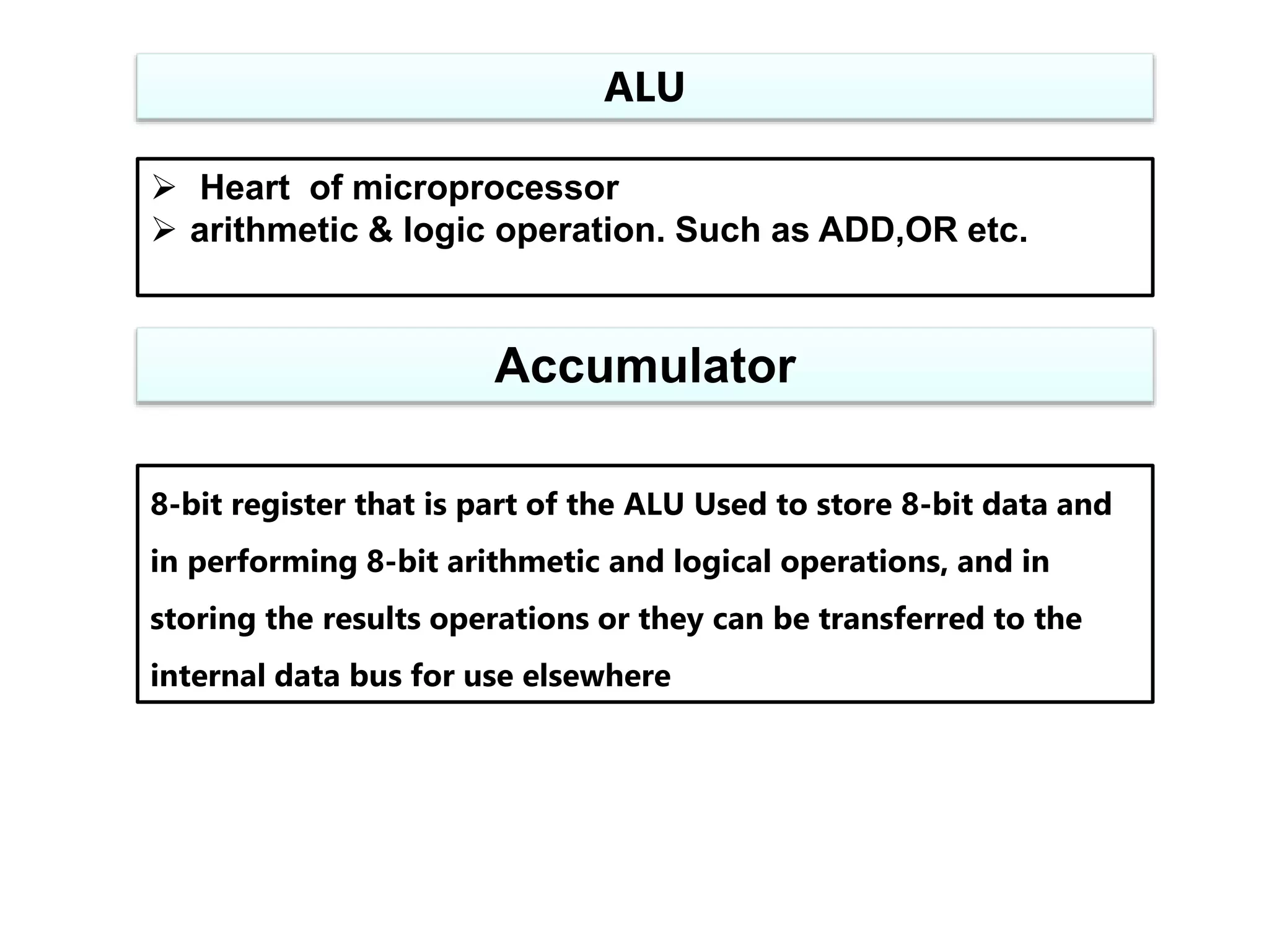
ALU
Heart ofmicroprocessor
arithmetic & logic operation. Such as ADD,OR etc.
Accumulator
8-bit register that is part of the ALU Used to store 8-bit data and
in performing 8-bit arithmetic and logical operations, and in
storing the results operations or they can be transferred to the
internal data bus for use elsewhere
AC-Auxiliary Carry
This flagis set when a carry is generated from bit D3
and passed to D4 . This flag is used only internally
for BCD operations.
P-Parity flag
After an ALU operation if the result has an
even no of 1’s the p-flag is set. Otherwise it
is cleared. So, the flag can be used to
indicate even parity.
34.
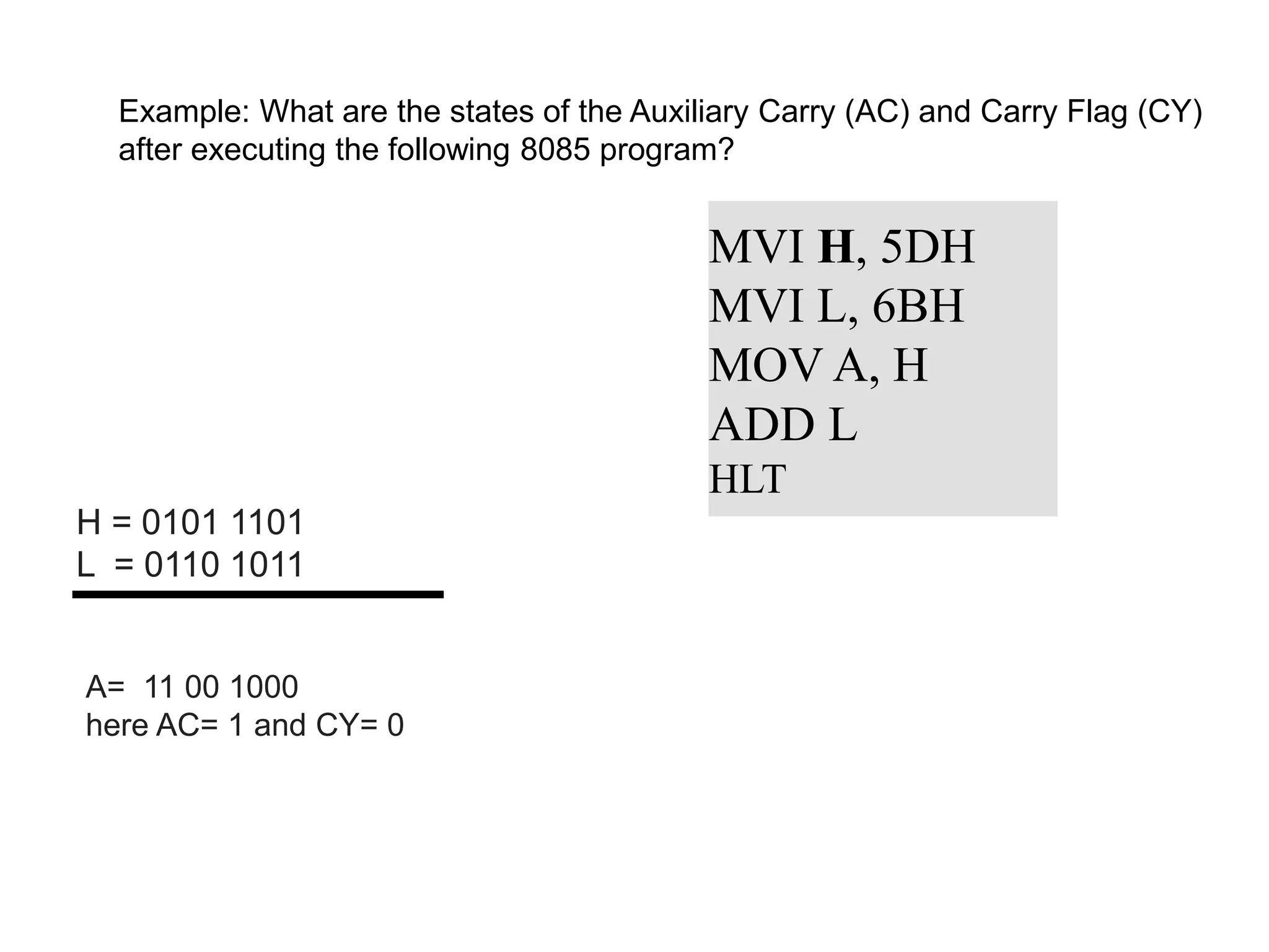
Example: What arethe states of the Auxiliary Carry (AC) and Carry Flag (CY)
after executing the following 8085 program?
MVI H, 5DH
MVI L, 6BH
MOV A, H
ADD L
HLT
H = 0101 1101
L = 0110 1011
A= 11 00 1000
here AC= 1 and CY= 0
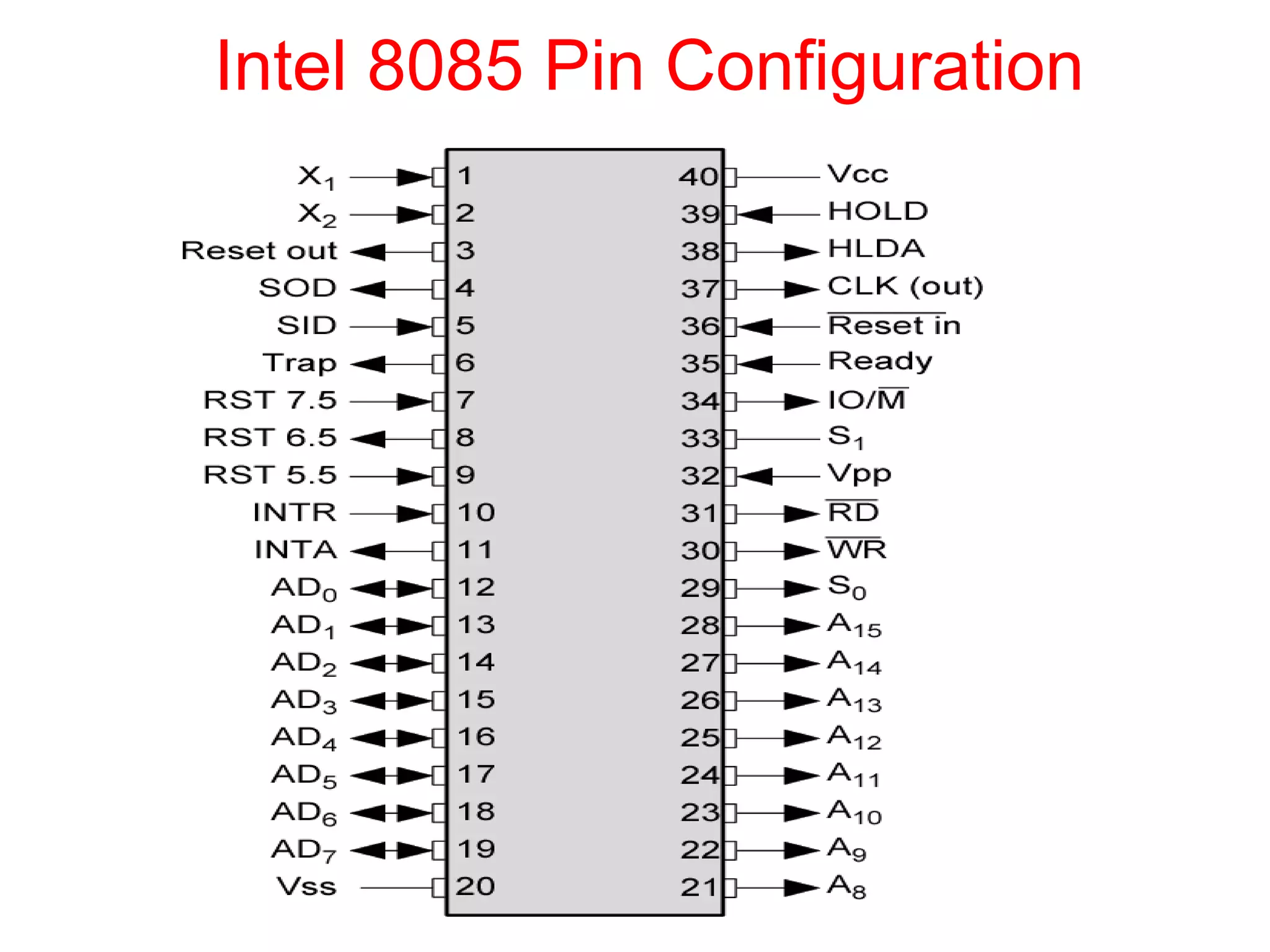
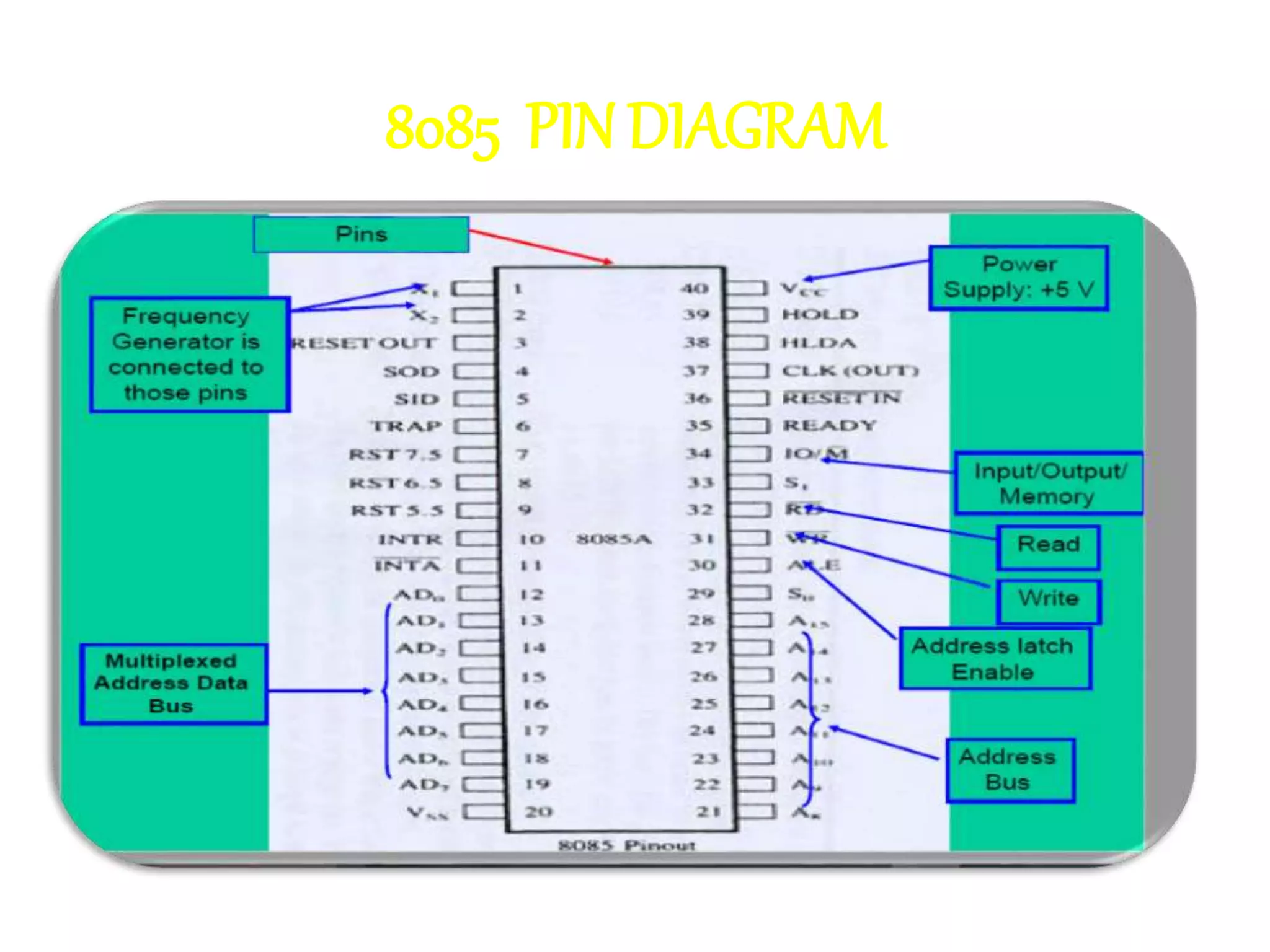
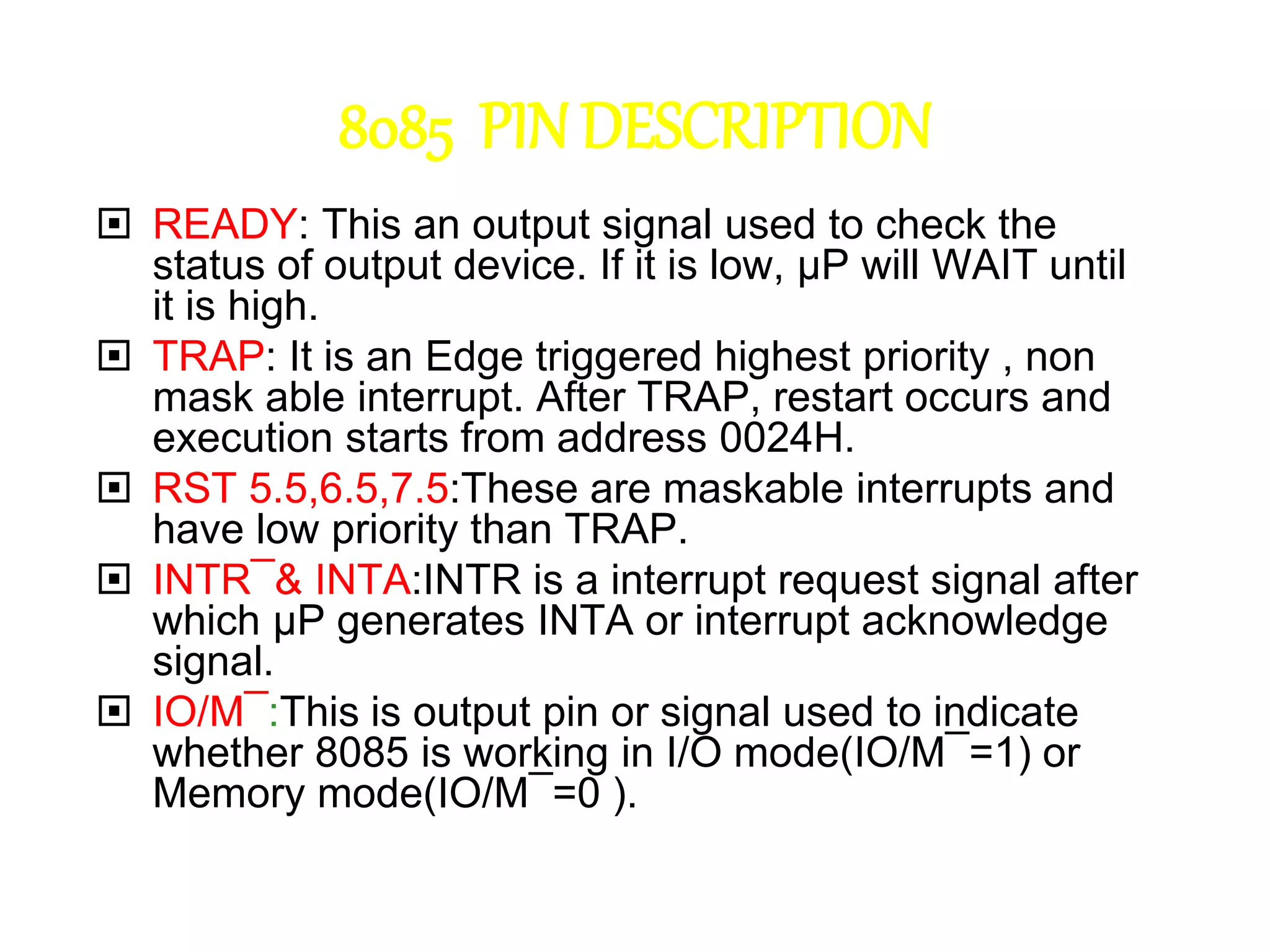
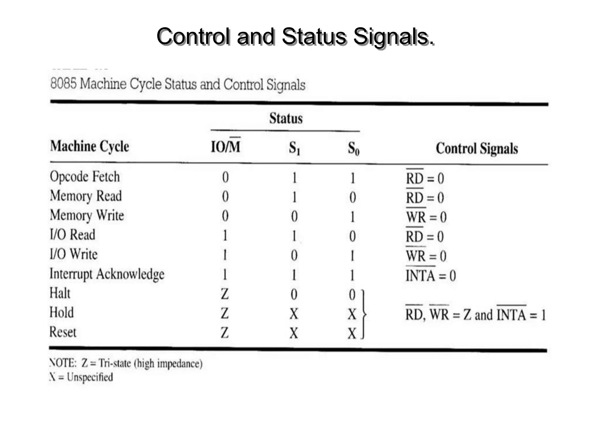
8085 PIN DESCRIPTION
READY: This an output signal used to check the
status of output device. If it is low, µP will WAIT until
it is high.
TRAP: It is an Edge triggered highest priority , non
mask able interrupt. After TRAP, restart occurs and
execution starts from address 0024H.
RST 5.5,6.5,7.5:These are maskable interrupts and
have low priority than TRAP.
INTR¯& INTA:INTR is a interrupt request signal after
which µP generates INTA or interrupt acknowledge
signal.
IO/M¯:This is output pin or signal used to indicate
whether 8085 is working in I/O mode(IO/M¯=1) or
Memory mode(IO/M¯=0 ).
42.
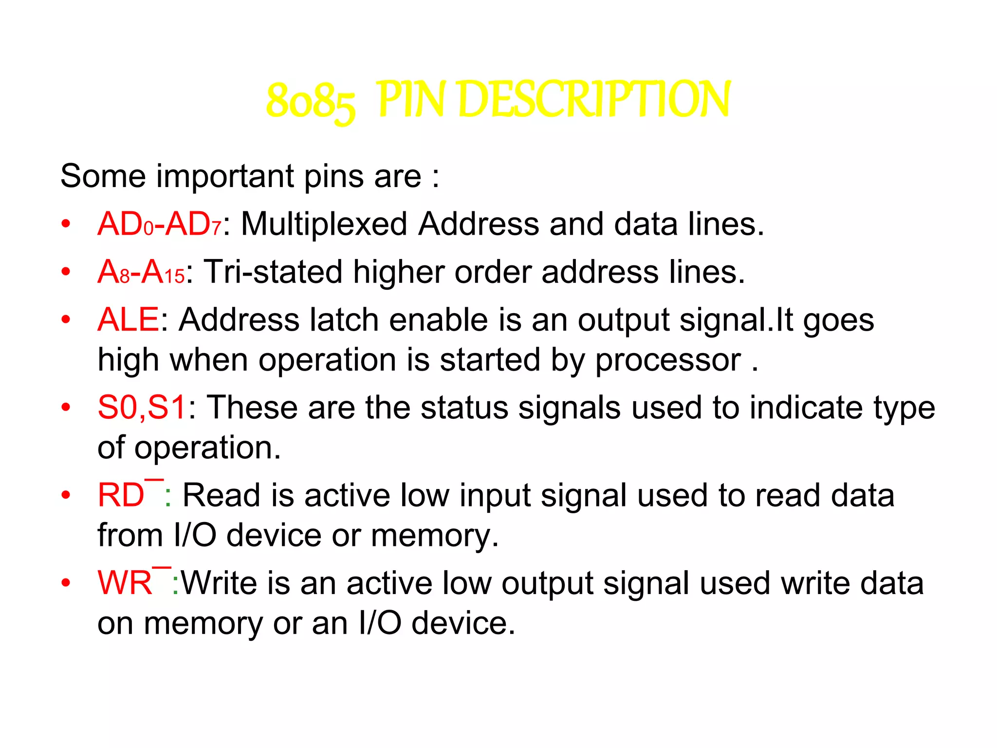
8085 PIN DESCRIPTION
Someimportant pins are :
• AD0-AD7: Multiplexed Address and data lines.
• A8-A15: Tri-stated higher order address lines.
• ALE: Address latch enable is an output signal.It goes
high when operation is started by processor .
• S0,S1: These are the status signals used to indicate type
of operation.
• RD¯: Read is active low input signal used to read data
from I/O device or memory.
• WR¯:Write is an active low output signal used write data
on memory or an I/O device.
43.
8085 PIN DESCRIPTION
HOLD & HLDA:HOLD is an input signal .When µP receives
HOLD signal it completes current machine cycle and stops
executing next instruction. In response to HOLD µP
generates HLDA that is HOLD Acknowledge signal.
RESET IN¯:This is input signal. When RESET IN¯ is low µp
restarts and starts executing from location 0000H.
SID: Serial input data is input pin used to accept serial 1 bit
data .
X1, X2 :These are clock input signals and are connected to
external LC, or RC circuit.These are divide by two so if 6
MHz is connected to X1X2, the operating frequency
becomes 3 MHz.
VCC & VSS:Power supply VCC=+5Volt & VSS=-GND
reference.
Direct Memory Access(DMA)
• DMA is an IO technique where external IO device
requests the use of the MPU buses.
• Allows external IO devices to gain high speed access to
the memory.
– Example of IO devices that use DMA: disk memory system.
• HOLD and HLDA are used for DMA.
• If HOLD=1, 8085 will place it address, data and control
pins at their high-impedance.
• A DMA acknowledgement is signaled by HLDA=1.
46.
46
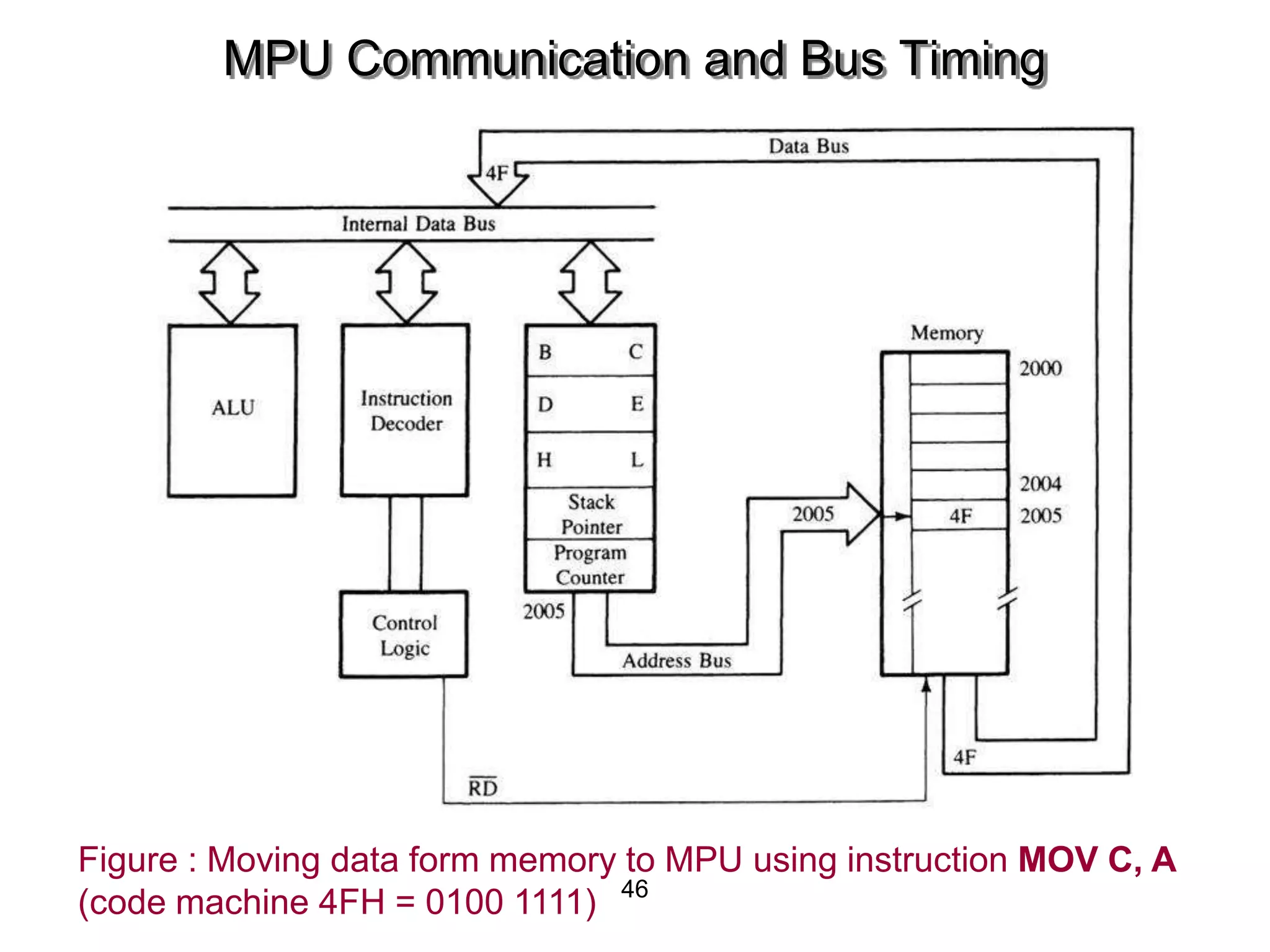
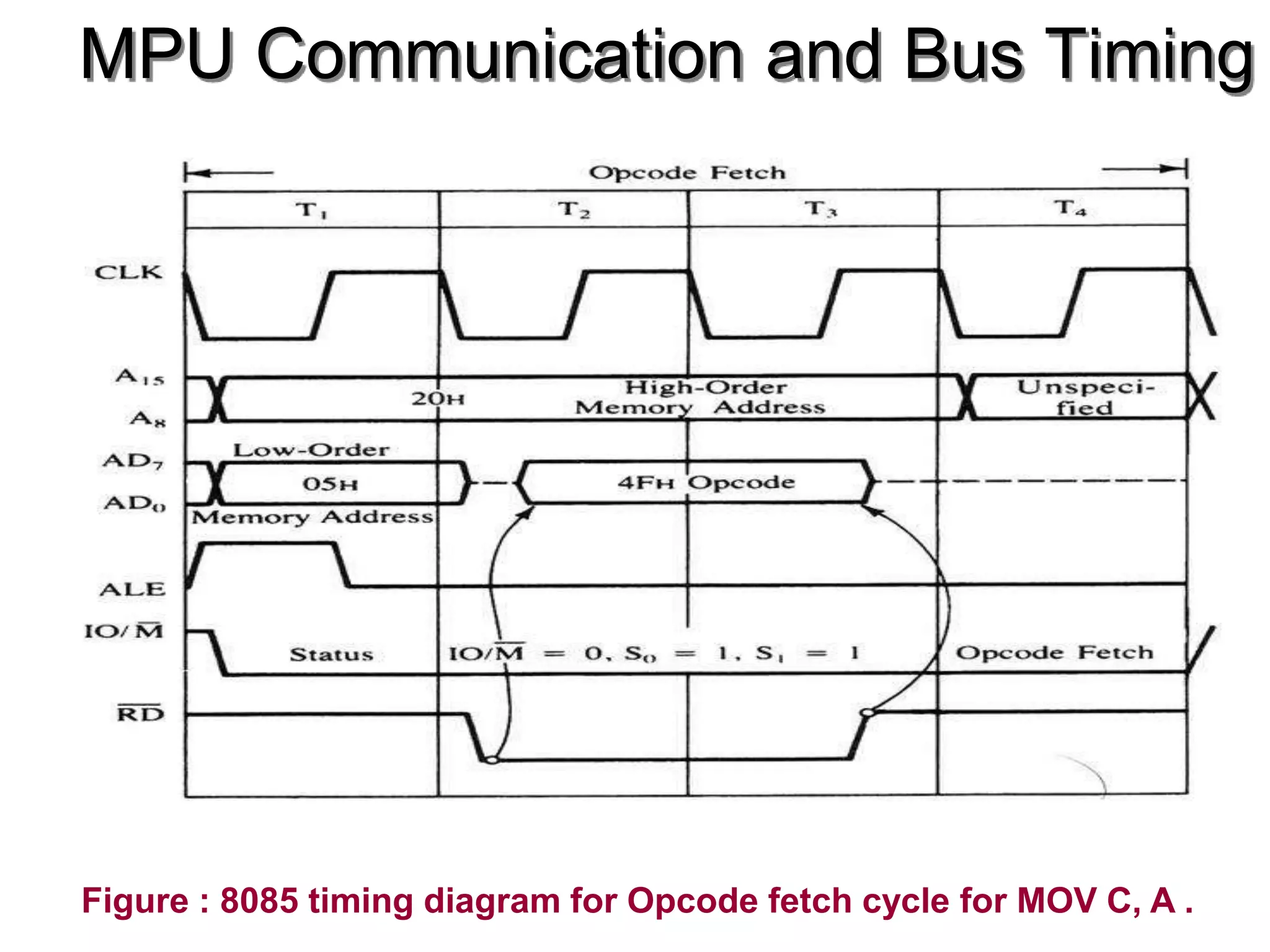
MPU Communication andBus Timing
Figure : Moving data form memory to MPU using instruction MOV C, A
(code machine 4FH = 0100 1111)
47.
47
• The FetchExecute Sequence :
1. The μp placed a 16 bit memory address from
PC (program counter) to address bus.
– Figure 4: at T1
– The high order address, 20H, is placed at A15 – A8.
– the low order address, 05H, is placed at AD7 - AD0 and
ALE is active high.
– Synchronously the IO/M is in active low condition to show it
is a memory operation.
2. At T2 the active low control signal, RD, is
activated so as to activate read operation; it is to
indicate that the MPU is in fetch mode
operation.
MPU Communication and Bus
Timing
48.
48
Figure : 8085timing diagram for Opcode fetch cycle for MOV C, A .
MPU Communication and Bus Timing