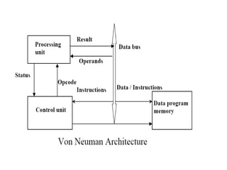
SlideShare a Scribd company logo
Microprocessor
• Microprocessor is the CPU of a Microcomputer.
• It is the heart of the micro computer.
• Microprocessor or is a silicon chip that contains a CPU. In the world
of personal computers, the terms microprocessor and CPU are used
interchangeably.
• A microprocessor (sometimes abbreviated μP) is a digital electronic
component with miniaturized transistors on a single semiconductor
integrated circuit (IC).
• One or more microprocessors typically serve as a central processing
unit (CPU) in a computer system or handheld device.
Microprocessor
• Microprocessors made possible the advent of
the microcomputer.
• At the heart of all personal computers and most
working stations sits a microprocessor.
• Microprocessors also control the logic of almost
all digital devices, from clock radios to fuel-
injection systems for automobiles.
Microprocessor’s Characteristics
Three basic characteristics differentiate microprocessors:
• Instruction set: The set of instructions that the
microprocessor can execute.
• Bandwidth: The number of bits processed in a single
instruction.
• Clock speed: Given in megahertz (MHz), the clock speed
determines how many instructions per second the
processor can execute.
Microcontroller
A highly integrated chip that contains all the components comprising a
controller.
• Typically this includes a CPU, RAM, some form of ROM, I/O ports,
and timers.
• Unlike a general-purpose computer, which also includes all of these
components, a microcontroller is designed for a very specific task -
to control a particular system.
• A microcontroller differs from a microprocessor, which is a general-
purpose chip that is used to create a multi-function computer or
device and requires multiple chips to handle various tasks.
•.
• A microcontroller is meant to be more self-contained and
independent, and functions as a tiny, dedicated computer.
• The great advantage of microcontrollers, as opposed to using larger
microprocessors, is that the parts-count and design costs of the item
being controlled can be kept to a minimum.
• They are typically designed using CMOS (complementary metal oxide
semiconductor) technology, an efficient fabrication technique that
uses less power and is more immune to power spikes than other
techniques.
• Microcontrollers are sometimes called embedded microcontrollers,
which just means that they are part of an embedded system that is,
one part of a larger device or system
Controller
A device that controls the transfer of data from a computer
to a peripheral device and vice versa.
• For example, disk drives, display screens, keyboards and
printers all require controllers.
• In personal computers, the controllers are often single
chips.
• When you purchase a computer, it comes with all the
necessary controllers for standard components, such as
the display screen, keyboard, and disk drives.
Difference
MICRO PROCESSER
• It is a CPU
• Memory, I/O Ports to be
connected externally
MICRO CONTROLLER
• It is a single chip
• Consists Memory, I/O
ports
BUS: A shared group of wires used for
communicating signals among devices.
– address bus: the device and the location within the
device that is being accessed
– data bus: the data value being communicated
– control bus: describes the action on the address
and data buses
CPU: Core of the processor, where instructions are
executed
– High-level language: a = b + c
– Assembly language: add r1 r2 r3
– Machine language: 0001001010111010101
Memory: Where instructions (programs) and data
are stored
– Organized in arrays of locations (addresses), each
storing one byte (8 bits) in general
– A read operation to a particular location always
returns the last value stored in that location
I/O devices: Enable system to interact with the
world.
– Device interface (a.k.a. controller or adapter)
hardware connects actual device to bus
– The CPU views the I/O device registers just like
memory that can be accessed over the bus.
However, I/O registers are connected to external
wires, device control logic, etc.
– Reads may not return last value written
– Writes may have side effects
Big-Endian and Little-Endian Storage
When data types having a word size larger than the smallest
addressable unit are stored in memory the question arises,
“Is the least significant part of the word stored at the
lowest address (little Endian, little end first) or–
is the most significant part of the word stored at the
lowest address (big Endian, big end first)”?
Example: The hexadecimal 16-bit number ABCDH, stored at address 0:
AB CD
msb ... lsb
AB
CD0
1
AB
CD
0
1
Little
Endian
Big Endian
von Neumann architecture
• The von Neumann architecture is a design model for a stored-program
digital computer that uses a central processing unit (CPU) and a single
separate storage structure ("memory") to hold both instructions and data. It
is named after the mathematician and early computer scientist John von
Neumann. Such computers implement a universal Turing machine and have
a sequential architecture.
• A stored-program digital computer is one that keeps its programmed
instructions, as well as its data, in read-write, random-access memory
(RAM). Stored-program computers were an advancement over the program-
controlled computers of the 1940s, such as the Colossus and the ENIAC,
which were programmed by setting switches and inserting patch leads to
route data and to control signals between various functional units. In the
vast majority of modern computers, the same memory is used for both data
and program instructions. The mechanisms for transferring the data and
instructions between the CPU and memory are, however, considerably more
complex than the original von Neumann architecture.
Harvard architecture
• The Harvard architecture is a computer architecture with physically
separate storage and signal pathways for instructions and data. The
term originated from the Harvard Mark I relay-based computer,
which stored instructions on punched tape (24 bits wide) and data in
electro-mechanical counters. These early machines had limited data
storage, entirely contained within the central processing unit, and
provided no access to the instruction storage as data. Programs
needed to be loaded by an operator, the processor could not boot
itself.
• Today, most processors implement such separate signal pathways
for performance reasons but actually implement a
Modified Harvard architecture, so they can support tasks like
loading a program from disk storage as data and then executing it.
Harvard architecture
Modified Harvard Architecture
• The Modified Harvard Architecture is a
variation of the Harvard computer
architecture that allows the contents of the
instruction memory to be accessed as if it
were data. Most modern computers that
are documented as Harvard Architecture
are, in fact, Modified Harvard Architecture.
Overview of 8085 microprocessor
– 8085 Architecture
1. Cpu of microcomputer
2. 8085 is 8 bit microprocessor
• Pin Diagram
1. 40 pin IC package fabricated on a single LSI
chip.
2. Uses a single +5V DC supply for its use.
• Functional Block Diagram
Intel 8085
• 8 bit NMOS Microprocessor.
• 40 pin IC fabrictaed on single LSI chip
• Uses a single +5v DC supply for its
operation
• Clock speed is 3Mhz.
• Clock cycle is of 320ns
• It has 80 basic instruction and 246
opcodes
Three main sections
• ALU
• A timing and Control unit
• Set of registers
ALU
• Perform the arithmetic operations
1. Addition
2. Subtraction
3. Logical AND
4. Logical OR
5. Logical Exclusive OR
6. Complement (Logical NOT)
7. Increment (add 1)
8. Decrement (Subtract 1)
9. Left Shift ,Rotate Left , Rotate right
10. Clear
Timing and Control unit
• Generates timing and control signals necessary to carry out the
instruction, which has been decoded.
• Control data path (flow) b/w CPU and peripheral (including memory).
• Provide status ,control and timing signals which are requested for the
operation of memory and I/O devices.
• Control entire operations of the microprocessor and peripheral connected
to it.
• CU is the brain of the computer.
• In reality causes certain connections between blocks of the uP to be
opened or closed, so that data goes where it is required, and so that ALU
operations occur.
24
The 8085 Bus Structure
The 8-bit 8085 CPU (or MPU – Micro Processing Unit)
communicates with the other units using a 16-bit address
bus, an 8-bit data bus and a control bus.
25
The 8085 Bus Structure
Address Bus
 Consists of 16 address lines: A0 – A15
 Operates in unidirectional mode: The address
bits are always sent from the MPU to peripheral
devices, not reverse.
 16 address lines are capable of addressing a
total of 216
= 65,536 (64k) memory locations.
 Address locations: 0000 (hex) – FFFF (hex)
26
The 8085 Bus Structure
Data Bus
 Consists of 8 data lines: D0 – D7
 Operates in bidirectional mode: The data bits are
sent from the MPU to peripheral devices, as well
as from the peripheral devices to the MPU.
 Data range: 00 (hex) – FF (hex)
Control Bus
 Consists of various lines carrying the control
signals such as read / write enable, flag bits.
Intel 8085 Registers
• It has following registers, registers are
small due to limited size of the chip:
• One 8-bit ACC (Accumulator).
• 6 Eight bit GPR (B,C,D,E,H and L).
• One 16 bit SP (Stack Pointer)
• One 16 bit PC (Program Counter)
• Instruction Register
• Temporary Register
Set of registers
• Used by the microprocessor for temporary storage and
manipulation of data and instruction.
• Programmer can use these registers to store or copy data into the
registers by using data copy instructions.
• Data remain in register till they are sent to the memory or I/O device.
• one accumulator,
• The 8085 has six general-purpose registers to store 8-bit data;
these are
identified as B,C,D,E,H, and L
• They can be combined as register pairs - BC, DE, and HL - to
perform some 16-bit operations.
• one flag register
• It has two 16-bit registers: the stack
pointer and the program counter.
• Large Computer have more registers so
program requires less transfer of data to/
from the memory.
• Small Computers have less register due to
limited size on chip.
Accumulator (ACC)
• 8 bit register.
• Register A
• Used for storing the operands/data during execution.
• Hold one of the operands of an arithmetic operation.
• Serve as an Input to the ALU.
• The other operand for an arithmetic operation may be stored in the memory or GPR.
• The final result of an operation is placed in the Acc.
• DAD rp for 16 bit addition for which one of the 16 bit operands is kept in H-L and the
other in the B-C or D-E pair. The result is placed in the H-L pair.
Program counter (PC)
• 16 bit special purpose register.
• Used to store the memory address of the next instruction to be executed.
• Keep track of the memory addresses of the instruction in a program while they are
being executed.
• Microprocessor increment the content of PC during the execution of the instruction So
that it points to the adress of the next instruction in the program at the end of the
execution of an instuction.
• Index register – This is used for addressing
index addressing mode.
• Stack pointer – It is a 16 bit register used to
initialize the stack.
• Instruction register – It is a 8 bit register that
stores the instruction fetched from memory
Status register
• The ALU includes five flip-flops, which are set or reset after an operation
according to data conditions of the result in the accumulator and other
registers.
• It stores the present status of the microprocessor after any arithmetic and
logical operation.
• It records any occurrence of carry, auxiliary carry, sign, zero and odd/even
parity.
• The five status flags of Intel 8085 are:
1. Carry Flag (CS)
2. Parity Flag (P)
3. Auxiliary Carry Flag (AC)
4. Zero Flag (Z)
5. Sign Flag (S)
AC (Auxiliary Carry)
• AC hold carry out of the bit number 3 to the bit number 4
resulting from the execution of an arithmetic operation.
• Counting of the bits starts from zero.
• ADD CB and E9
C B = 1100 1011
E 9 = 1110 1001
1011 0100
CY =1
MSB =1 ; S=1
AC =1
Four 1’s ; P=1
Result is non zero ; Z=0
Buses
• It is the interface section for communication between processor and
external devices. There are 3 buses
1. Address bus – It carries the address of the instruction. It is 16 bit
wide and unidirectional.
2. Data bus – It carries data between external devices and processor.
It is 8 bit wide and bidirectional.
3. Control bus – It is used to send control signals to different units of
microprocessor.
8085 Pin description.
Properties
• Single + 5V Supply
• 4 Vectored Interrupts (One is Non Mask able)
• Serial In/Serial Out Port
• Decimal, Binary, and Double Precision Arithmetic
• Direct Addressing Capability to 64K bytes of memory
• The Intel 8085A is a new generation, complete 8 bit
parallel central processing unit (CPU).
• The 8085A uses a multiplexed data bus.
• The address is split between the 8bit address bus and
the 8bit data bus. Figures are at the end of the
document.
Pin Description
The following describes the function of each pin:
• A8 – 16 (Output 3 State): Address Bus; The
most significant 8 bits of the memory address or
the 8 bits of the I/0 address,3 stated during Hold
and Halt modes.
• AD0 - 7 (Input/Output 3state) : Multiplexed
Address/Data Bus; Lower 8 bits of the memory
address (or I/0 address) appear on the bus
during the first clock cycle of a machine state. It
then becomes the data bus during the second
and third clock cycles. 3 stated during Hold and
Halt modes.
• ALE (Output) Address Latch Enable: It occurs during the first clock
cycle of a machine state and enables the address to get latched into
the on chip latch of peripherals.
• The falling edge of ALE is set to guarantee setup and hold times for
the address information.
• ALE can also be used to strobe the status information. ALE is never
3stated.
• SO, S1 (Output)
Data Bus Status. Encoded status of the bus cycle:
1. S1 S0
2. O O HALT
3. 0 1 WRITE
4. 1 0 READ
5. 1 1 FETCH
• S1 can be used as an advanced R/W status.
• RD (Output 3state): READ; indicates the selected
memory or 1/0 device is to be read and that the Data
Bus is available for the data transfer.
• WR (Output 3state):WRITE; indicates the data on the
Data Bus is to be written into the selected memory or 1/0
location. Data is set up at the trailing edge of WR.
3stated during Hold and Halt modes.
• READY (Input): If Ready is high during a read or write
cycle, it indicates that the memory or peripheral is ready
to send or receive data. If Ready is low, the CPU will
wait for
• Ready to go high before completing the read or write
cycle.
• HOLD (Input) :
HOLD; indicates that another Master is requesting the
use of the Address and Data Buses. The CPU, upon
receiving the Hold request. will relinquish the use of
buses as soon as the completion of the current machine
cycle. Internal processing can continue. The processor
can regain the buses only after the Hold is removed.
When the Hold is acknowledged, the Address, Data, RD,
WR, and IO/M lines are 3stated.
• HLDA (Output) :
HOLD ACKNOWLEDGE; indicates that the CPU has
received the Hold request and that it will relinquish the
buses in the next clock cycle. HLDA goes low after the
Hold request is removed. The CPU takes the buses one
half clock cycle after HLDA goes low.
• INTR (Input): INTERRUPT REQUEST; is used as a
general purpose interrupt. It is sampled only during the
next to the last clock cycle of the instruction. If it is
active, the Program Counter (PC) will be inhibited from
incrementing and an INTA will be issued. During this
cycle a RESTART or CALL instruction can be inserted to
jump to the interrupt service routine. The INTR is
enabled and disabled by software. It is disabled by Reset
and immediately after an interrupt is accepted.
• INTA (Output): INTERRUPT ACKNOWLEDGE; is used
instead of (and has the same timing as) RD
• during the Instruction cycle after an INTR is accepted. It
can be used to activate the
• 8259 Interrupt chip or some other interrupt port.
• RST 5.5
• RST 6.5 - (Inputs)
• RST 7.5
RESTART INTERRUPTS:These three inputs have the same
timing as I NTR except they cause an internal RESTART to be
automatically inserted.
RST 7.5 ~~ Highest Priority
RST 6.5
RST 5.5 o Lowest Priority
The priority of these interrupts is ordered as shown above.
These interrupts have a higher priority than the INTR.
•TRAP (Input): Trap interrupt is a non-mask able restart
interrupt. It is recognized at the same time as INTR. It is
unaffected by any mask or Interrupt Enable. It has the highest
priority of any interrupt.
• RESET IN (Input):
Reset sets the Program Counter to zero and resets the
Interrupt Enable and HLDA flipflops. None of the other
flags or registers (except the instruction register) are
affected The CPU is held in the reset condition as long
as Reset is applied.
• RESET OUT (Output):
Indicates CPU is being reset. Can be used as a system
RESET. The signal is synchronized to the processor
clock.
• X1, X2 (Input):
Crystal or R/C network connections to set the internal
clock generator X1 can also be an external clock input
instead of a crystal. The input frequency is divided by 2
to give the internal operating frequency.
• SOD (output): Serial output data line. The
output SOD is set or reset as specified by
the SIM instruction.
• Vcc: +5 volt supply.
• Vss: Ground Reference.
• CLK (Output): Clock Output for use as a
system clock when a crystal or R/ C
network is used as an input to the CPU.
The period of CLK is twice the X1, X2
input period.
• IO/M (Output): IO/M indicates whether the
Read/Write is to memory or l/O Tristated
during Hold and Halt modes.
• SID (Input): Serial input data line The data
on this line is loaded into accumulator bit 7
whenever a RIM instruction is executed.
49
The 8085: CPU Internal Structure
The internal architecture of the 8085 CPU is
capable of performing the following operations:
 Store 8-bit data (Registers, Accumulator)
 Perform arithmetic and logic operations (ALU)
 Test for conditions (IF / THEN)
 Sequence the execution of instructions
 Store temporary data in RAM during execution
50
The 8085: CPU Internal Structure
Simplified block diagram
51
Example: Memory Read Operation
52
Example: Instruction Fetch Operation
 All instructions (program steps) are stored in memory.
 To run a program, the individual instructions must
be read from the memory in sequence, and executed.
 Program counter puts the 16-bit memory address of the
instruction on the address bus
 Control unit sends the Memory Read Enable signal to
access the memory
 The 8-bit instruction stored in memory is placed on the data
bus and transferred to the instruction decoder
 Instruction is decoded and executed
53
Example: Instruction Fetch Operation
54
Example: Instruction Fetch Operation
55
8085 Functional Block Diagram
Addressing modes
• The data are specified in different modes in the
instructions. The various ways of specifying data are
called addressing modes.
• The 8085 microprocessor has 5 types of addressing
modes
1. Immediate Addressing mode
2. Register Addressing mode
3. Direct Addressing mode
4. Indirect Addressing mode
5. Implied Addressing mode
Immediate Addressing mode :
• When the data is directly specified in the
instruction, Which is called immediate
addressing mode.( MVI reg, Data)
Example:
MVI B, 72H
LXI H,5000H
Register Addressing mode
• When the data is stored in the register and
if the register is specified in the instruction,
then it is called register addressing mode .
( MOV Rd., Rs).
• Eg: MOV D, C;
The contents of C is moved to register D.
Direct Addressing mode
• When the memory Address specified with
in the instruction, then it is called direct
addressing mode.
Eg: LDA 5000H;
The 5000H memory content is stored in to
the accumulator.
Indirect Addressing mode
• Load the data , to the accumulator from the
memory. The data which is pointed by the
memory pointer (HL reg),it is called indirect
addressing mode.
• Example:
MOV A, M
The data moved to accumulator from the
memory, which is pointed by the memory
pointer.
Implied Addressing mode
• When the instruction itself specifies the
data to be operated, then it is called
Implied addressing mode.
Example:
CMA - Complement the content of
accumulator.
RRC- rotate accumulator content with out
carry.
Data Transfer Group:
The data transfer instructions move data between registers or between
memory and registers.
• MOV : Move
• MVI : Move Immediate
• LDA :Load Accumulator Directly from Memory
• STA :Store Accumulator Directly in Memory
• LHLD: Load H & L Registers Directly from Memory
• SHLD : Store H & L Registers Directly in Memory
• An 'X' in the name of a data transfer instruction implies that it deals with a
register pair (16-bits);
• LXI : Load Register Pair with Immediate data
• LDAX : Load Accumulator from Address in
Register Pair
• STAX : Store Accumulator in Address in
Register Pair
• XCHG : Exchange H & L with D & E
• XTHL :Exchange Top of Stack with H & L
Arithmetic Group Instructions
• The arithmetic instructions add, subtract, increment, or
decrement data in registers or memory.
• ADD Add to Accumulator
• ADI Add Immediate Data to Accumulator
• ADC Add to Accumulator Using Carry Flag
• ACI Add Immediate data to Accumulator Using
Carry
• SUB Subtract from Accumulator
• SUI Subtract Immediate Data from Accumulator
• SBB Subtract from Accumulator Using Borrow
(Carry) Flag
• SBI Subtract Immediate from Accumulator Using
Borrow (Carry) Flag
• INR Increment Specified Byte by One
• DCR Decrement Specified Byte by One
• INX Increment Register Pair by One
• DCX Decrement Register Pair by One
• DAD Double Register Add; Add Content of
Register Pair to H & L Register Pair
Logical Group
• This group performs logical (Boolean) operations on data in registers
and memory and on condition flags.
• The logical AND, OR, and Exclusive OR instructions enable you to set
specific bits in the accumulator ON or OFF.
• ANA Logical AND with Accumulator
• ANI Logical AND with Accumulator Using Immediate Data
• ORA Logical OR with Accumulator
• OR Logical OR with Accumulator Using Immediate Data
• XRA Exclusive Logical OR with Accumulator
• XRI Exclusive OR Using Immediate Data
• The Compare instructions compare the content of an 8-bit value with the
contents of the accumulator;
• CMP Compare
• CPI Compare Using Immediate Data
• The rotate instructions shift the contents of the accumulator one bit
position to the left or right:
•
• RLC Rotate Accumulator Left
• RRC Rotate Accumulator Right
• RAL Rotate Left Through Carry
• RAR Rotate Right Through Carry
• Complement and carry flag instructions:
•
• CMA Complement Accumulator
• CMC Complement Carry Flag
• STC Set Carry Flag
Branch Group Instructions
• The branching instructions alter normal
sequential program flow, either
unconditionally or conditionally. The
unconditional branching instructions are
as follows:
• JMP Jump
• CALL Call
• RET Return
Conditional branching instructions examine the status
of one of four condition flags to determine whether
the specified branch is to be executed.
The conditions that may be specified are as follows:
• NZ Not Zero (Z = 0)
• Z Zero (Z = 1)
• NC No Carry (C = 0)
• C Carry (C = 1)
• PO Parity Odd (P = 0)
• PE Parity Even (P = 1)
• P Plus (S = 0)
• M Minus (S = 1)
• Thus, the conditional branching instructions are
specified as follows:
Jumps Calls Returns
1. C CC RC (Carry)
2. INC CNC RNC (No Carry)
3. JZ CZ RZ (Zero)
4. JNZ CNZ RNZ (Not Zero)
5. JP CP RP (Plus)
6. JM CM RM (Minus)
7. JPE CPE RPE (Parity Even)
8. JP0 CPO RPO (Parity Odd)
• Two other instructions can affect a branch
by replacing the contents or the program
counter:
• PCHL Move H & L to Program
Counter
• RST Special Restart Instruction
Used with Interrupts
Stack I/O and Machine Control
Instructions
• Stack I/O, and Machine Control Instructions:
• The following instructions affect the Stack
and/or Stack Pointer:
•
• PUSH Push Two bytes of Data onto the
Stack
• POP Pop Two Bytes of Data off the Stack
• XTHL Exchange Top of Stack with H & L
• SPHL Move content of H & L to Stack
Pointer
• The I/0 instructions are as follows:
• IN Initiate Input Operation
• OUT Initiate Output Operation
• The Machine Control instructions are
as follows:
• EI Enable Interrupt System
• DI Disable Interrupt System
• HLT Halt
• NOP No Operation

More Related Content

What's hot

Memory system
Memory systemMemory system
Memory system
gourav kottawar
 
Introduction to Microcontroller
Introduction to MicrocontrollerIntroduction to Microcontroller
Introduction to Microcontroller
Nikhil Sharma
 
Overview of microcontroller and microprocessor
Overview of microcontroller and microprocessor Overview of microcontroller and microprocessor
Overview of microcontroller and microprocessor
Mrunal Deshkar
 
RISC - Reduced Instruction Set Computing
RISC - Reduced Instruction Set ComputingRISC - Reduced Instruction Set Computing
RISC - Reduced Instruction Set Computing
Tushar Swami
 
TMS320C5x
TMS320C5xTMS320C5x
PIC Microcontrollers.ppt
PIC Microcontrollers.pptPIC Microcontrollers.ppt
PIC Microcontrollers.ppt
Dr.YNM
 
8086-instruction-set-ppt
 8086-instruction-set-ppt 8086-instruction-set-ppt
8086-instruction-set-pptjemimajerome
 
Memory & I/O interfacing
Memory & I/O  interfacingMemory & I/O  interfacing
Memory & I/O interfacing
deval patel
 
Direct Memory Access
Direct Memory AccessDirect Memory Access
Direct Memory Access
Hetauda City College
 
Memory interfacing
Memory interfacingMemory interfacing
Memory interfacing
mahalakshmimalini
 
Introduction to microcontroller
Introduction to microcontrollerIntroduction to microcontroller
Introduction to microcontroller
Rajib Roy
 
ARM Processors
ARM ProcessorsARM Processors
ARM Processors
Mathivanan Natarajan
 
Module 1 8086
Module 1 8086Module 1 8086
Module 1 8086
Deepak John
 
Basic Computer Architecture
Basic Computer ArchitectureBasic Computer Architecture
Basic Computer Architecture
Yong Heui Cho
 
Memories in digital electronics
Memories in digital electronicsMemories in digital electronics
Memories in digital electronics
SijuGeorge10
 
8085 microproceesor ppt
8085 microproceesor ppt8085 microproceesor ppt
8085 microproceesor ppt
RJ Aniket
 
8051 block diagram
8051 block diagram8051 block diagram
8051 block diagram
DominicHendry
 
8251 USART
8251 USART8251 USART
8251 USART
coolsdhanesh
 

What's hot (20)

Memory system
Memory systemMemory system
Memory system
 
Introduction to Microcontroller
Introduction to MicrocontrollerIntroduction to Microcontroller
Introduction to Microcontroller
 
Overview of microcontroller and microprocessor
Overview of microcontroller and microprocessor Overview of microcontroller and microprocessor
Overview of microcontroller and microprocessor
 
RISC - Reduced Instruction Set Computing
RISC - Reduced Instruction Set ComputingRISC - Reduced Instruction Set Computing
RISC - Reduced Instruction Set Computing
 
8086
80868086
8086
 
TMS320C5x
TMS320C5xTMS320C5x
TMS320C5x
 
Lecture 3 instruction set
Lecture 3  instruction setLecture 3  instruction set
Lecture 3 instruction set
 
PIC Microcontrollers.ppt
PIC Microcontrollers.pptPIC Microcontrollers.ppt
PIC Microcontrollers.ppt
 
8086-instruction-set-ppt
 8086-instruction-set-ppt 8086-instruction-set-ppt
8086-instruction-set-ppt
 
Memory & I/O interfacing
Memory & I/O  interfacingMemory & I/O  interfacing
Memory & I/O interfacing
 
Direct Memory Access
Direct Memory AccessDirect Memory Access
Direct Memory Access
 
Memory interfacing
Memory interfacingMemory interfacing
Memory interfacing
 
Introduction to microcontroller
Introduction to microcontrollerIntroduction to microcontroller
Introduction to microcontroller
 
ARM Processors
ARM ProcessorsARM Processors
ARM Processors
 
Module 1 8086
Module 1 8086Module 1 8086
Module 1 8086
 
Basic Computer Architecture
Basic Computer ArchitectureBasic Computer Architecture
Basic Computer Architecture
 
Memories in digital electronics
Memories in digital electronicsMemories in digital electronics
Memories in digital electronics
 
8085 microproceesor ppt
8085 microproceesor ppt8085 microproceesor ppt
8085 microproceesor ppt
 
8051 block diagram
8051 block diagram8051 block diagram
8051 block diagram
 
8251 USART
8251 USART8251 USART
8251 USART
 

Viewers also liked

39245203 intro-es-iv
39245203 intro-es-iv39245203 intro-es-iv
39245203 intro-es-ivEmbeddedbvp
 
39245175 intro-es-ii
39245175 intro-es-ii39245175 intro-es-ii
39245175 intro-es-iiEmbeddedbvp
 
39245196 intro-es-iii
39245196 intro-es-iii39245196 intro-es-iii
39245196 intro-es-iiiEmbeddedbvp
 
39245147 intro-es-i
39245147 intro-es-i39245147 intro-es-i
39245147 intro-es-iEmbeddedbvp
 
постоюк н.а.
постоюк н.а.постоюк н.а.
постоюк н.а.natalichka25
 
Facebook building fanlets & pages
Facebook   building fanlets & pagesFacebook   building fanlets & pages
Facebook building fanlets & pagesEngage121
 
Local social overview
Local social overviewLocal social overview
Local social overviewEngage121
 
коаксиальный кабель
коаксиальный кабелькоаксиальный кабель
коаксиальный кабельlisitca
 
Nokia 002 l4d0 n86 unlocked phone with 8 mp camera auto focus flash and carl ...
Nokia 002 l4d0 n86 unlocked phone with 8 mp camera auto focus flash and carl ...Nokia 002 l4d0 n86 unlocked phone with 8 mp camera auto focus flash and carl ...
Nokia 002 l4d0 n86 unlocked phone with 8 mp camera auto focus flash and carl ...Tancheasere
 
витая пара.строение.преминение
витая пара.строение.преминениевитая пара.строение.преминение
витая пара.строение.преминениеlisitca
 
Apresentação1
Apresentação1Apresentação1
Apresentação1
kleberjuninho
 
Engage121 - Paid Media - June 2014
Engage121 - Paid Media - June 2014Engage121 - Paid Media - June 2014
Engage121 - Paid Media - June 2014Engage121
 
Engage121 customer service - june 2014
Engage121   customer service - june 2014Engage121   customer service - june 2014
Engage121 customer service - june 2014Engage121
 

Viewers also liked (16)

39245203 intro-es-iv
39245203 intro-es-iv39245203 intro-es-iv
39245203 intro-es-iv
 
39245175 intro-es-ii
39245175 intro-es-ii39245175 intro-es-ii
39245175 intro-es-ii
 
39245196 intro-es-iii
39245196 intro-es-iii39245196 intro-es-iii
39245196 intro-es-iii
 
39245147 intro-es-i
39245147 intro-es-i39245147 intro-es-i
39245147 intro-es-i
 
Srer report-b-2
Srer report-b-2Srer report-b-2
Srer report-b-2
 
постоюк н.а.
постоюк н.а.постоюк н.а.
постоюк н.а.
 
Facebook building fanlets & pages
Facebook   building fanlets & pagesFacebook   building fanlets & pages
Facebook building fanlets & pages
 
Local social overview
Local social overviewLocal social overview
Local social overview
 
коаксиальный кабель
коаксиальный кабелькоаксиальный кабель
коаксиальный кабель
 
Nokia 002 l4d0 n86 unlocked phone with 8 mp camera auto focus flash and carl ...
Nokia 002 l4d0 n86 unlocked phone with 8 mp camera auto focus flash and carl ...Nokia 002 l4d0 n86 unlocked phone with 8 mp camera auto focus flash and carl ...
Nokia 002 l4d0 n86 unlocked phone with 8 mp camera auto focus flash and carl ...
 
витая пара.строение.преминение
витая пара.строение.преминениевитая пара.строение.преминение
витая пара.строение.преминение
 
big-data-better-data-white-paper-final
big-data-better-data-white-paper-finalbig-data-better-data-white-paper-final
big-data-better-data-white-paper-final
 
Apresentação1
Apresentação1Apresentação1
Apresentação1
 
Engage121 - Paid Media - June 2014
Engage121 - Paid Media - June 2014Engage121 - Paid Media - June 2014
Engage121 - Paid Media - June 2014
 
Engage121 customer service - june 2014
Engage121   customer service - june 2014Engage121   customer service - june 2014
Engage121 customer service - june 2014
 
Infor1
Infor1Infor1
Infor1
 

Similar to Microprocessor

Micro controller
Micro controllerMicro controller
Micro controller
Devi Prasad
 
Processors
ProcessorsProcessors
Processors
HIMANSHU JAIN
 
I. Introduction to Microprocessor System.ppt
I. Introduction to Microprocessor System.pptI. Introduction to Microprocessor System.ppt
I. Introduction to Microprocessor System.ppt
HAriesOa1
 
1. Introduction to Microprocessor.pptx
1. Introduction to Microprocessor.pptx1. Introduction to Microprocessor.pptx
1. Introduction to Microprocessor.pptx
ISMT College
 
Unit 1. introduction
Unit 1. introductionUnit 1. introduction
Unit 1. introduction
Kiran Bagale
 
Module -4_microprocessor (1).pptx
Module -4_microprocessor (1).pptxModule -4_microprocessor (1).pptx
Module -4_microprocessor (1).pptx
DrVaibhavMeshram
 
micro controllers 1.ppt
micro controllers 1.pptmicro controllers 1.ppt
micro controllers 1.ppt
siminkhan
 
Micro controller and dsp processor
Micro controller and dsp processorMicro controller and dsp processor
Micro controller and dsp processor
ShubhamMishra485
 
LECT 2.pptx
LECT 2.pptxLECT 2.pptx
LECT 2.pptx
SangeetaTripathi8
 
introduction to microprocessors
introduction to microprocessorsintroduction to microprocessors
introduction to microprocessors
sudheerkethamreddy
 
4CS3-MPI-Unit-1.pptx
4CS3-MPI-Unit-1.pptx4CS3-MPI-Unit-1.pptx
4CS3-MPI-Unit-1.pptx
Lofi19
 
PILOT Session for Embedded Systems
PILOT Session for Embedded Systems PILOT Session for Embedded Systems
PILOT Session for Embedded Systems
Mohamed Al-Emam, PMP®, CAP®
 
8051 microcontroller
8051 microcontroller8051 microcontroller
8051 microcontrollersnehapvs
 
MergeResult_2023_04_02_05_26_56.pptx
MergeResult_2023_04_02_05_26_56.pptxMergeResult_2023_04_02_05_26_56.pptx
MergeResult_2023_04_02_05_26_56.pptx
bhaveshagrawal35
 
introduction of microprocessor
introduction of microprocessorintroduction of microprocessor
introduction of microprocessor
Reetika Singh
 
Sistem mikroprosessor
Sistem mikroprosessorSistem mikroprosessor
Sistem mikroprosessorfahmihafid
 
Microprocessor fundamentals
Microprocessor fundamentalsMicroprocessor fundamentals
Microprocessor fundamentals
JLoknathDora
 
Mechatronics ME8791
Mechatronics ME8791 Mechatronics ME8791
Mechatronics ME8791
DrPETERPRAKASH
 
Introduction to embedded System.pptx
Introduction to embedded System.pptxIntroduction to embedded System.pptx
Introduction to embedded System.pptx
Pratik Gohel
 
Embedded systems 101 final
Embedded systems 101 finalEmbedded systems 101 final
Embedded systems 101 final
Khalid Elmeadawy
 

Similar to Microprocessor (20)

Micro controller
Micro controllerMicro controller
Micro controller
 
Processors
ProcessorsProcessors
Processors
 
I. Introduction to Microprocessor System.ppt
I. Introduction to Microprocessor System.pptI. Introduction to Microprocessor System.ppt
I. Introduction to Microprocessor System.ppt
 
1. Introduction to Microprocessor.pptx
1. Introduction to Microprocessor.pptx1. Introduction to Microprocessor.pptx
1. Introduction to Microprocessor.pptx
 
Unit 1. introduction
Unit 1. introductionUnit 1. introduction
Unit 1. introduction
 
Module -4_microprocessor (1).pptx
Module -4_microprocessor (1).pptxModule -4_microprocessor (1).pptx
Module -4_microprocessor (1).pptx
 
micro controllers 1.ppt
micro controllers 1.pptmicro controllers 1.ppt
micro controllers 1.ppt
 
Micro controller and dsp processor
Micro controller and dsp processorMicro controller and dsp processor
Micro controller and dsp processor
 
LECT 2.pptx
LECT 2.pptxLECT 2.pptx
LECT 2.pptx
 
introduction to microprocessors
introduction to microprocessorsintroduction to microprocessors
introduction to microprocessors
 
4CS3-MPI-Unit-1.pptx
4CS3-MPI-Unit-1.pptx4CS3-MPI-Unit-1.pptx
4CS3-MPI-Unit-1.pptx
 
PILOT Session for Embedded Systems
PILOT Session for Embedded Systems PILOT Session for Embedded Systems
PILOT Session for Embedded Systems
 
8051 microcontroller
8051 microcontroller8051 microcontroller
8051 microcontroller
 
MergeResult_2023_04_02_05_26_56.pptx
MergeResult_2023_04_02_05_26_56.pptxMergeResult_2023_04_02_05_26_56.pptx
MergeResult_2023_04_02_05_26_56.pptx
 
introduction of microprocessor
introduction of microprocessorintroduction of microprocessor
introduction of microprocessor
 
Sistem mikroprosessor
Sistem mikroprosessorSistem mikroprosessor
Sistem mikroprosessor
 
Microprocessor fundamentals
Microprocessor fundamentalsMicroprocessor fundamentals
Microprocessor fundamentals
 
Mechatronics ME8791
Mechatronics ME8791 Mechatronics ME8791
Mechatronics ME8791
 
Introduction to embedded System.pptx
Introduction to embedded System.pptxIntroduction to embedded System.pptx
Introduction to embedded System.pptx
 
Embedded systems 101 final
Embedded systems 101 finalEmbedded systems 101 final
Embedded systems 101 final
 

Recently uploaded

GenAISummit 2024 May 28 Sri Ambati Keynote: AGI Belongs to The Community in O...
GenAISummit 2024 May 28 Sri Ambati Keynote: AGI Belongs to The Community in O...GenAISummit 2024 May 28 Sri Ambati Keynote: AGI Belongs to The Community in O...
GenAISummit 2024 May 28 Sri Ambati Keynote: AGI Belongs to The Community in O...
Sri Ambati
 
Leading Change strategies and insights for effective change management pdf 1.pdf
Leading Change strategies and insights for effective change management pdf 1.pdfLeading Change strategies and insights for effective change management pdf 1.pdf
Leading Change strategies and insights for effective change management pdf 1.pdf
OnBoard
 
FIDO Alliance Osaka Seminar: Passkeys at Amazon.pdf
FIDO Alliance Osaka Seminar: Passkeys at Amazon.pdfFIDO Alliance Osaka Seminar: Passkeys at Amazon.pdf
FIDO Alliance Osaka Seminar: Passkeys at Amazon.pdf
FIDO Alliance
 
Essentials of Automations: Optimizing FME Workflows with Parameters
Essentials of Automations: Optimizing FME Workflows with ParametersEssentials of Automations: Optimizing FME Workflows with Parameters
Essentials of Automations: Optimizing FME Workflows with Parameters
Safe Software
 
Smart TV Buyer Insights Survey 2024 by 91mobiles.pdf
Smart TV Buyer Insights Survey 2024 by 91mobiles.pdfSmart TV Buyer Insights Survey 2024 by 91mobiles.pdf
Smart TV Buyer Insights Survey 2024 by 91mobiles.pdf
91mobiles
 
Slack (or Teams) Automation for Bonterra Impact Management (fka Social Soluti...
Slack (or Teams) Automation for Bonterra Impact Management (fka Social Soluti...Slack (or Teams) Automation for Bonterra Impact Management (fka Social Soluti...
Slack (or Teams) Automation for Bonterra Impact Management (fka Social Soluti...
Jeffrey Haguewood
 
How world-class product teams are winning in the AI era by CEO and Founder, P...
How world-class product teams are winning in the AI era by CEO and Founder, P...How world-class product teams are winning in the AI era by CEO and Founder, P...
How world-class product teams are winning in the AI era by CEO and Founder, P...
Product School
 
JMeter webinar - integration with InfluxDB and Grafana
JMeter webinar - integration with InfluxDB and GrafanaJMeter webinar - integration with InfluxDB and Grafana
JMeter webinar - integration with InfluxDB and Grafana
RTTS
 
Bits & Pixels using AI for Good.........
Bits & Pixels using AI for Good.........Bits & Pixels using AI for Good.........
Bits & Pixels using AI for Good.........
Alison B. Lowndes
 
Search and Society: Reimagining Information Access for Radical Futures
Search and Society: Reimagining Information Access for Radical FuturesSearch and Society: Reimagining Information Access for Radical Futures
Search and Society: Reimagining Information Access for Radical Futures
Bhaskar Mitra
 
Assuring Contact Center Experiences for Your Customers With ThousandEyes
Assuring Contact Center Experiences for Your Customers With ThousandEyesAssuring Contact Center Experiences for Your Customers With ThousandEyes
Assuring Contact Center Experiences for Your Customers With ThousandEyes
ThousandEyes
 
PHP Frameworks: I want to break free (IPC Berlin 2024)
PHP Frameworks: I want to break free (IPC Berlin 2024)PHP Frameworks: I want to break free (IPC Berlin 2024)
PHP Frameworks: I want to break free (IPC Berlin 2024)
Ralf Eggert
 
De-mystifying Zero to One: Design Informed Techniques for Greenfield Innovati...
De-mystifying Zero to One: Design Informed Techniques for Greenfield Innovati...De-mystifying Zero to One: Design Informed Techniques for Greenfield Innovati...
De-mystifying Zero to One: Design Informed Techniques for Greenfield Innovati...
Product School
 
Empowering NextGen Mobility via Large Action Model Infrastructure (LAMI): pav...
Empowering NextGen Mobility via Large Action Model Infrastructure (LAMI): pav...Empowering NextGen Mobility via Large Action Model Infrastructure (LAMI): pav...
Empowering NextGen Mobility via Large Action Model Infrastructure (LAMI): pav...
Thierry Lestable
 
ODC, Data Fabric and Architecture User Group
ODC, Data Fabric and Architecture User GroupODC, Data Fabric and Architecture User Group
ODC, Data Fabric and Architecture User Group
CatarinaPereira64715
 
Mission to Decommission: Importance of Decommissioning Products to Increase E...
Mission to Decommission: Importance of Decommissioning Products to Increase E...Mission to Decommission: Importance of Decommissioning Products to Increase E...
Mission to Decommission: Importance of Decommissioning Products to Increase E...
Product School
 
FIDO Alliance Osaka Seminar: Overview.pdf
FIDO Alliance Osaka Seminar: Overview.pdfFIDO Alliance Osaka Seminar: Overview.pdf
FIDO Alliance Osaka Seminar: Overview.pdf
FIDO Alliance
 
FIDO Alliance Osaka Seminar: The WebAuthn API and Discoverable Credentials.pdf
FIDO Alliance Osaka Seminar: The WebAuthn API and Discoverable Credentials.pdfFIDO Alliance Osaka Seminar: The WebAuthn API and Discoverable Credentials.pdf
FIDO Alliance Osaka Seminar: The WebAuthn API and Discoverable Credentials.pdf
FIDO Alliance
 
The Art of the Pitch: WordPress Relationships and Sales
The Art of the Pitch: WordPress Relationships and SalesThe Art of the Pitch: WordPress Relationships and Sales
The Art of the Pitch: WordPress Relationships and Sales
Laura Byrne
 
The Future of Platform Engineering
The Future of Platform EngineeringThe Future of Platform Engineering
The Future of Platform Engineering
Jemma Hussein Allen
 

Recently uploaded (20)

GenAISummit 2024 May 28 Sri Ambati Keynote: AGI Belongs to The Community in O...
GenAISummit 2024 May 28 Sri Ambati Keynote: AGI Belongs to The Community in O...GenAISummit 2024 May 28 Sri Ambati Keynote: AGI Belongs to The Community in O...
GenAISummit 2024 May 28 Sri Ambati Keynote: AGI Belongs to The Community in O...
 
Leading Change strategies and insights for effective change management pdf 1.pdf
Leading Change strategies and insights for effective change management pdf 1.pdfLeading Change strategies and insights for effective change management pdf 1.pdf
Leading Change strategies and insights for effective change management pdf 1.pdf
 
FIDO Alliance Osaka Seminar: Passkeys at Amazon.pdf
FIDO Alliance Osaka Seminar: Passkeys at Amazon.pdfFIDO Alliance Osaka Seminar: Passkeys at Amazon.pdf
FIDO Alliance Osaka Seminar: Passkeys at Amazon.pdf
 
Essentials of Automations: Optimizing FME Workflows with Parameters
Essentials of Automations: Optimizing FME Workflows with ParametersEssentials of Automations: Optimizing FME Workflows with Parameters
Essentials of Automations: Optimizing FME Workflows with Parameters
 
Smart TV Buyer Insights Survey 2024 by 91mobiles.pdf
Smart TV Buyer Insights Survey 2024 by 91mobiles.pdfSmart TV Buyer Insights Survey 2024 by 91mobiles.pdf
Smart TV Buyer Insights Survey 2024 by 91mobiles.pdf
 
Slack (or Teams) Automation for Bonterra Impact Management (fka Social Soluti...
Slack (or Teams) Automation for Bonterra Impact Management (fka Social Soluti...Slack (or Teams) Automation for Bonterra Impact Management (fka Social Soluti...
Slack (or Teams) Automation for Bonterra Impact Management (fka Social Soluti...
 
How world-class product teams are winning in the AI era by CEO and Founder, P...
How world-class product teams are winning in the AI era by CEO and Founder, P...How world-class product teams are winning in the AI era by CEO and Founder, P...
How world-class product teams are winning in the AI era by CEO and Founder, P...
 
JMeter webinar - integration with InfluxDB and Grafana
JMeter webinar - integration with InfluxDB and GrafanaJMeter webinar - integration with InfluxDB and Grafana
JMeter webinar - integration with InfluxDB and Grafana
 
Bits & Pixels using AI for Good.........
Bits & Pixels using AI for Good.........Bits & Pixels using AI for Good.........
Bits & Pixels using AI for Good.........
 
Search and Society: Reimagining Information Access for Radical Futures
Search and Society: Reimagining Information Access for Radical FuturesSearch and Society: Reimagining Information Access for Radical Futures
Search and Society: Reimagining Information Access for Radical Futures
 
Assuring Contact Center Experiences for Your Customers With ThousandEyes
Assuring Contact Center Experiences for Your Customers With ThousandEyesAssuring Contact Center Experiences for Your Customers With ThousandEyes
Assuring Contact Center Experiences for Your Customers With ThousandEyes
 
PHP Frameworks: I want to break free (IPC Berlin 2024)
PHP Frameworks: I want to break free (IPC Berlin 2024)PHP Frameworks: I want to break free (IPC Berlin 2024)
PHP Frameworks: I want to break free (IPC Berlin 2024)
 
De-mystifying Zero to One: Design Informed Techniques for Greenfield Innovati...
De-mystifying Zero to One: Design Informed Techniques for Greenfield Innovati...De-mystifying Zero to One: Design Informed Techniques for Greenfield Innovati...
De-mystifying Zero to One: Design Informed Techniques for Greenfield Innovati...
 
Empowering NextGen Mobility via Large Action Model Infrastructure (LAMI): pav...
Empowering NextGen Mobility via Large Action Model Infrastructure (LAMI): pav...Empowering NextGen Mobility via Large Action Model Infrastructure (LAMI): pav...
Empowering NextGen Mobility via Large Action Model Infrastructure (LAMI): pav...
 
ODC, Data Fabric and Architecture User Group
ODC, Data Fabric and Architecture User GroupODC, Data Fabric and Architecture User Group
ODC, Data Fabric and Architecture User Group
 
Mission to Decommission: Importance of Decommissioning Products to Increase E...
Mission to Decommission: Importance of Decommissioning Products to Increase E...Mission to Decommission: Importance of Decommissioning Products to Increase E...
Mission to Decommission: Importance of Decommissioning Products to Increase E...
 
FIDO Alliance Osaka Seminar: Overview.pdf
FIDO Alliance Osaka Seminar: Overview.pdfFIDO Alliance Osaka Seminar: Overview.pdf
FIDO Alliance Osaka Seminar: Overview.pdf
 
FIDO Alliance Osaka Seminar: The WebAuthn API and Discoverable Credentials.pdf
FIDO Alliance Osaka Seminar: The WebAuthn API and Discoverable Credentials.pdfFIDO Alliance Osaka Seminar: The WebAuthn API and Discoverable Credentials.pdf
FIDO Alliance Osaka Seminar: The WebAuthn API and Discoverable Credentials.pdf
 
The Art of the Pitch: WordPress Relationships and Sales
The Art of the Pitch: WordPress Relationships and SalesThe Art of the Pitch: WordPress Relationships and Sales
The Art of the Pitch: WordPress Relationships and Sales
 
The Future of Platform Engineering
The Future of Platform EngineeringThe Future of Platform Engineering
The Future of Platform Engineering
 

Microprocessor

  • 1. Microprocessor • Microprocessor is the CPU of a Microcomputer. • It is the heart of the micro computer. • Microprocessor or is a silicon chip that contains a CPU. In the world of personal computers, the terms microprocessor and CPU are used interchangeably. • A microprocessor (sometimes abbreviated μP) is a digital electronic component with miniaturized transistors on a single semiconductor integrated circuit (IC). • One or more microprocessors typically serve as a central processing unit (CPU) in a computer system or handheld device.
  • 2. Microprocessor • Microprocessors made possible the advent of the microcomputer. • At the heart of all personal computers and most working stations sits a microprocessor. • Microprocessors also control the logic of almost all digital devices, from clock radios to fuel- injection systems for automobiles.
  • 3. Microprocessor’s Characteristics Three basic characteristics differentiate microprocessors: • Instruction set: The set of instructions that the microprocessor can execute. • Bandwidth: The number of bits processed in a single instruction. • Clock speed: Given in megahertz (MHz), the clock speed determines how many instructions per second the processor can execute.
  • 4. Microcontroller A highly integrated chip that contains all the components comprising a controller. • Typically this includes a CPU, RAM, some form of ROM, I/O ports, and timers. • Unlike a general-purpose computer, which also includes all of these components, a microcontroller is designed for a very specific task - to control a particular system. • A microcontroller differs from a microprocessor, which is a general- purpose chip that is used to create a multi-function computer or device and requires multiple chips to handle various tasks. •.
  • 5. • A microcontroller is meant to be more self-contained and independent, and functions as a tiny, dedicated computer. • The great advantage of microcontrollers, as opposed to using larger microprocessors, is that the parts-count and design costs of the item being controlled can be kept to a minimum. • They are typically designed using CMOS (complementary metal oxide semiconductor) technology, an efficient fabrication technique that uses less power and is more immune to power spikes than other techniques. • Microcontrollers are sometimes called embedded microcontrollers, which just means that they are part of an embedded system that is, one part of a larger device or system
  • 6. Controller A device that controls the transfer of data from a computer to a peripheral device and vice versa. • For example, disk drives, display screens, keyboards and printers all require controllers. • In personal computers, the controllers are often single chips. • When you purchase a computer, it comes with all the necessary controllers for standard components, such as the display screen, keyboard, and disk drives.
  • 7. Difference MICRO PROCESSER • It is a CPU • Memory, I/O Ports to be connected externally MICRO CONTROLLER • It is a single chip • Consists Memory, I/O ports
  • 8. BUS: A shared group of wires used for communicating signals among devices. – address bus: the device and the location within the device that is being accessed – data bus: the data value being communicated – control bus: describes the action on the address and data buses CPU: Core of the processor, where instructions are executed – High-level language: a = b + c – Assembly language: add r1 r2 r3 – Machine language: 0001001010111010101
  • 9. Memory: Where instructions (programs) and data are stored – Organized in arrays of locations (addresses), each storing one byte (8 bits) in general – A read operation to a particular location always returns the last value stored in that location I/O devices: Enable system to interact with the world. – Device interface (a.k.a. controller or adapter) hardware connects actual device to bus – The CPU views the I/O device registers just like memory that can be accessed over the bus. However, I/O registers are connected to external wires, device control logic, etc. – Reads may not return last value written – Writes may have side effects
  • 10. Big-Endian and Little-Endian Storage When data types having a word size larger than the smallest addressable unit are stored in memory the question arises, “Is the least significant part of the word stored at the lowest address (little Endian, little end first) or– is the most significant part of the word stored at the lowest address (big Endian, big end first)”? Example: The hexadecimal 16-bit number ABCDH, stored at address 0: AB CD msb ... lsb AB CD0 1 AB CD 0 1 Little Endian Big Endian
  • 11. von Neumann architecture • The von Neumann architecture is a design model for a stored-program digital computer that uses a central processing unit (CPU) and a single separate storage structure ("memory") to hold both instructions and data. It is named after the mathematician and early computer scientist John von Neumann. Such computers implement a universal Turing machine and have a sequential architecture. • A stored-program digital computer is one that keeps its programmed instructions, as well as its data, in read-write, random-access memory (RAM). Stored-program computers were an advancement over the program- controlled computers of the 1940s, such as the Colossus and the ENIAC, which were programmed by setting switches and inserting patch leads to route data and to control signals between various functional units. In the vast majority of modern computers, the same memory is used for both data and program instructions. The mechanisms for transferring the data and instructions between the CPU and memory are, however, considerably more complex than the original von Neumann architecture.
  • 12.
  • 13.
  • 14. Harvard architecture • The Harvard architecture is a computer architecture with physically separate storage and signal pathways for instructions and data. The term originated from the Harvard Mark I relay-based computer, which stored instructions on punched tape (24 bits wide) and data in electro-mechanical counters. These early machines had limited data storage, entirely contained within the central processing unit, and provided no access to the instruction storage as data. Programs needed to be loaded by an operator, the processor could not boot itself. • Today, most processors implement such separate signal pathways for performance reasons but actually implement a Modified Harvard architecture, so they can support tasks like loading a program from disk storage as data and then executing it.
  • 16.
  • 17. Modified Harvard Architecture • The Modified Harvard Architecture is a variation of the Harvard computer architecture that allows the contents of the instruction memory to be accessed as if it were data. Most modern computers that are documented as Harvard Architecture are, in fact, Modified Harvard Architecture.
  • 18.
  • 19. Overview of 8085 microprocessor – 8085 Architecture 1. Cpu of microcomputer 2. 8085 is 8 bit microprocessor • Pin Diagram 1. 40 pin IC package fabricated on a single LSI chip. 2. Uses a single +5V DC supply for its use. • Functional Block Diagram
  • 20. Intel 8085 • 8 bit NMOS Microprocessor. • 40 pin IC fabrictaed on single LSI chip • Uses a single +5v DC supply for its operation • Clock speed is 3Mhz. • Clock cycle is of 320ns • It has 80 basic instruction and 246 opcodes
  • 21. Three main sections • ALU • A timing and Control unit • Set of registers
  • 22. ALU • Perform the arithmetic operations 1. Addition 2. Subtraction 3. Logical AND 4. Logical OR 5. Logical Exclusive OR 6. Complement (Logical NOT) 7. Increment (add 1) 8. Decrement (Subtract 1) 9. Left Shift ,Rotate Left , Rotate right 10. Clear
  • 23. Timing and Control unit • Generates timing and control signals necessary to carry out the instruction, which has been decoded. • Control data path (flow) b/w CPU and peripheral (including memory). • Provide status ,control and timing signals which are requested for the operation of memory and I/O devices. • Control entire operations of the microprocessor and peripheral connected to it. • CU is the brain of the computer. • In reality causes certain connections between blocks of the uP to be opened or closed, so that data goes where it is required, and so that ALU operations occur.
  • 24. 24 The 8085 Bus Structure The 8-bit 8085 CPU (or MPU – Micro Processing Unit) communicates with the other units using a 16-bit address bus, an 8-bit data bus and a control bus.
  • 25. 25 The 8085 Bus Structure Address Bus  Consists of 16 address lines: A0 – A15  Operates in unidirectional mode: The address bits are always sent from the MPU to peripheral devices, not reverse.  16 address lines are capable of addressing a total of 216 = 65,536 (64k) memory locations.  Address locations: 0000 (hex) – FFFF (hex)
  • 26. 26 The 8085 Bus Structure Data Bus  Consists of 8 data lines: D0 – D7  Operates in bidirectional mode: The data bits are sent from the MPU to peripheral devices, as well as from the peripheral devices to the MPU.  Data range: 00 (hex) – FF (hex) Control Bus  Consists of various lines carrying the control signals such as read / write enable, flag bits.
  • 27. Intel 8085 Registers • It has following registers, registers are small due to limited size of the chip: • One 8-bit ACC (Accumulator). • 6 Eight bit GPR (B,C,D,E,H and L). • One 16 bit SP (Stack Pointer) • One 16 bit PC (Program Counter) • Instruction Register • Temporary Register
  • 28. Set of registers • Used by the microprocessor for temporary storage and manipulation of data and instruction. • Programmer can use these registers to store or copy data into the registers by using data copy instructions. • Data remain in register till they are sent to the memory or I/O device. • one accumulator, • The 8085 has six general-purpose registers to store 8-bit data; these are identified as B,C,D,E,H, and L • They can be combined as register pairs - BC, DE, and HL - to perform some 16-bit operations. • one flag register
  • 29. • It has two 16-bit registers: the stack pointer and the program counter. • Large Computer have more registers so program requires less transfer of data to/ from the memory. • Small Computers have less register due to limited size on chip.
  • 30. Accumulator (ACC) • 8 bit register. • Register A • Used for storing the operands/data during execution. • Hold one of the operands of an arithmetic operation. • Serve as an Input to the ALU. • The other operand for an arithmetic operation may be stored in the memory or GPR. • The final result of an operation is placed in the Acc. • DAD rp for 16 bit addition for which one of the 16 bit operands is kept in H-L and the other in the B-C or D-E pair. The result is placed in the H-L pair.
  • 31. Program counter (PC) • 16 bit special purpose register. • Used to store the memory address of the next instruction to be executed. • Keep track of the memory addresses of the instruction in a program while they are being executed. • Microprocessor increment the content of PC during the execution of the instruction So that it points to the adress of the next instruction in the program at the end of the execution of an instuction.
  • 32. • Index register – This is used for addressing index addressing mode. • Stack pointer – It is a 16 bit register used to initialize the stack. • Instruction register – It is a 8 bit register that stores the instruction fetched from memory
  • 33. Status register • The ALU includes five flip-flops, which are set or reset after an operation according to data conditions of the result in the accumulator and other registers. • It stores the present status of the microprocessor after any arithmetic and logical operation. • It records any occurrence of carry, auxiliary carry, sign, zero and odd/even parity. • The five status flags of Intel 8085 are: 1. Carry Flag (CS) 2. Parity Flag (P) 3. Auxiliary Carry Flag (AC) 4. Zero Flag (Z) 5. Sign Flag (S)
  • 34. AC (Auxiliary Carry) • AC hold carry out of the bit number 3 to the bit number 4 resulting from the execution of an arithmetic operation. • Counting of the bits starts from zero. • ADD CB and E9 C B = 1100 1011 E 9 = 1110 1001 1011 0100 CY =1 MSB =1 ; S=1 AC =1 Four 1’s ; P=1 Result is non zero ; Z=0
  • 35.
  • 36. Buses • It is the interface section for communication between processor and external devices. There are 3 buses 1. Address bus – It carries the address of the instruction. It is 16 bit wide and unidirectional. 2. Data bus – It carries data between external devices and processor. It is 8 bit wide and bidirectional. 3. Control bus – It is used to send control signals to different units of microprocessor.
  • 37.
  • 38. 8085 Pin description. Properties • Single + 5V Supply • 4 Vectored Interrupts (One is Non Mask able) • Serial In/Serial Out Port • Decimal, Binary, and Double Precision Arithmetic • Direct Addressing Capability to 64K bytes of memory • The Intel 8085A is a new generation, complete 8 bit parallel central processing unit (CPU). • The 8085A uses a multiplexed data bus. • The address is split between the 8bit address bus and the 8bit data bus. Figures are at the end of the document.
  • 39. Pin Description The following describes the function of each pin: • A8 – 16 (Output 3 State): Address Bus; The most significant 8 bits of the memory address or the 8 bits of the I/0 address,3 stated during Hold and Halt modes. • AD0 - 7 (Input/Output 3state) : Multiplexed Address/Data Bus; Lower 8 bits of the memory address (or I/0 address) appear on the bus during the first clock cycle of a machine state. It then becomes the data bus during the second and third clock cycles. 3 stated during Hold and Halt modes.
  • 40. • ALE (Output) Address Latch Enable: It occurs during the first clock cycle of a machine state and enables the address to get latched into the on chip latch of peripherals. • The falling edge of ALE is set to guarantee setup and hold times for the address information. • ALE can also be used to strobe the status information. ALE is never 3stated. • SO, S1 (Output) Data Bus Status. Encoded status of the bus cycle: 1. S1 S0 2. O O HALT 3. 0 1 WRITE 4. 1 0 READ 5. 1 1 FETCH • S1 can be used as an advanced R/W status.
  • 41. • RD (Output 3state): READ; indicates the selected memory or 1/0 device is to be read and that the Data Bus is available for the data transfer. • WR (Output 3state):WRITE; indicates the data on the Data Bus is to be written into the selected memory or 1/0 location. Data is set up at the trailing edge of WR. 3stated during Hold and Halt modes. • READY (Input): If Ready is high during a read or write cycle, it indicates that the memory or peripheral is ready to send or receive data. If Ready is low, the CPU will wait for • Ready to go high before completing the read or write cycle.
  • 42. • HOLD (Input) : HOLD; indicates that another Master is requesting the use of the Address and Data Buses. The CPU, upon receiving the Hold request. will relinquish the use of buses as soon as the completion of the current machine cycle. Internal processing can continue. The processor can regain the buses only after the Hold is removed. When the Hold is acknowledged, the Address, Data, RD, WR, and IO/M lines are 3stated. • HLDA (Output) : HOLD ACKNOWLEDGE; indicates that the CPU has received the Hold request and that it will relinquish the buses in the next clock cycle. HLDA goes low after the Hold request is removed. The CPU takes the buses one half clock cycle after HLDA goes low.
  • 43. • INTR (Input): INTERRUPT REQUEST; is used as a general purpose interrupt. It is sampled only during the next to the last clock cycle of the instruction. If it is active, the Program Counter (PC) will be inhibited from incrementing and an INTA will be issued. During this cycle a RESTART or CALL instruction can be inserted to jump to the interrupt service routine. The INTR is enabled and disabled by software. It is disabled by Reset and immediately after an interrupt is accepted. • INTA (Output): INTERRUPT ACKNOWLEDGE; is used instead of (and has the same timing as) RD • during the Instruction cycle after an INTR is accepted. It can be used to activate the • 8259 Interrupt chip or some other interrupt port. • RST 5.5 • RST 6.5 - (Inputs) • RST 7.5
  • 44. RESTART INTERRUPTS:These three inputs have the same timing as I NTR except they cause an internal RESTART to be automatically inserted. RST 7.5 ~~ Highest Priority RST 6.5 RST 5.5 o Lowest Priority The priority of these interrupts is ordered as shown above. These interrupts have a higher priority than the INTR. •TRAP (Input): Trap interrupt is a non-mask able restart interrupt. It is recognized at the same time as INTR. It is unaffected by any mask or Interrupt Enable. It has the highest priority of any interrupt.
  • 45. • RESET IN (Input): Reset sets the Program Counter to zero and resets the Interrupt Enable and HLDA flipflops. None of the other flags or registers (except the instruction register) are affected The CPU is held in the reset condition as long as Reset is applied. • RESET OUT (Output): Indicates CPU is being reset. Can be used as a system RESET. The signal is synchronized to the processor clock. • X1, X2 (Input): Crystal or R/C network connections to set the internal clock generator X1 can also be an external clock input instead of a crystal. The input frequency is divided by 2 to give the internal operating frequency.
  • 46. • SOD (output): Serial output data line. The output SOD is set or reset as specified by the SIM instruction. • Vcc: +5 volt supply. • Vss: Ground Reference.
  • 47. • CLK (Output): Clock Output for use as a system clock when a crystal or R/ C network is used as an input to the CPU. The period of CLK is twice the X1, X2 input period. • IO/M (Output): IO/M indicates whether the Read/Write is to memory or l/O Tristated during Hold and Halt modes. • SID (Input): Serial input data line The data on this line is loaded into accumulator bit 7 whenever a RIM instruction is executed.
  • 48.
  • 49. 49 The 8085: CPU Internal Structure The internal architecture of the 8085 CPU is capable of performing the following operations:  Store 8-bit data (Registers, Accumulator)  Perform arithmetic and logic operations (ALU)  Test for conditions (IF / THEN)  Sequence the execution of instructions  Store temporary data in RAM during execution
  • 50. 50 The 8085: CPU Internal Structure Simplified block diagram
  • 52. 52 Example: Instruction Fetch Operation  All instructions (program steps) are stored in memory.  To run a program, the individual instructions must be read from the memory in sequence, and executed.  Program counter puts the 16-bit memory address of the instruction on the address bus  Control unit sends the Memory Read Enable signal to access the memory  The 8-bit instruction stored in memory is placed on the data bus and transferred to the instruction decoder  Instruction is decoded and executed
  • 56. Addressing modes • The data are specified in different modes in the instructions. The various ways of specifying data are called addressing modes. • The 8085 microprocessor has 5 types of addressing modes 1. Immediate Addressing mode 2. Register Addressing mode 3. Direct Addressing mode 4. Indirect Addressing mode 5. Implied Addressing mode
  • 57. Immediate Addressing mode : • When the data is directly specified in the instruction, Which is called immediate addressing mode.( MVI reg, Data) Example: MVI B, 72H LXI H,5000H
  • 58. Register Addressing mode • When the data is stored in the register and if the register is specified in the instruction, then it is called register addressing mode . ( MOV Rd., Rs). • Eg: MOV D, C; The contents of C is moved to register D.
  • 59. Direct Addressing mode • When the memory Address specified with in the instruction, then it is called direct addressing mode. Eg: LDA 5000H; The 5000H memory content is stored in to the accumulator.
  • 60. Indirect Addressing mode • Load the data , to the accumulator from the memory. The data which is pointed by the memory pointer (HL reg),it is called indirect addressing mode. • Example: MOV A, M The data moved to accumulator from the memory, which is pointed by the memory pointer.
  • 61. Implied Addressing mode • When the instruction itself specifies the data to be operated, then it is called Implied addressing mode. Example: CMA - Complement the content of accumulator. RRC- rotate accumulator content with out carry.
  • 62. Data Transfer Group: The data transfer instructions move data between registers or between memory and registers. • MOV : Move • MVI : Move Immediate • LDA :Load Accumulator Directly from Memory • STA :Store Accumulator Directly in Memory • LHLD: Load H & L Registers Directly from Memory • SHLD : Store H & L Registers Directly in Memory • An 'X' in the name of a data transfer instruction implies that it deals with a register pair (16-bits);
  • 63. • LXI : Load Register Pair with Immediate data • LDAX : Load Accumulator from Address in Register Pair • STAX : Store Accumulator in Address in Register Pair • XCHG : Exchange H & L with D & E • XTHL :Exchange Top of Stack with H & L
  • 64. Arithmetic Group Instructions • The arithmetic instructions add, subtract, increment, or decrement data in registers or memory. • ADD Add to Accumulator • ADI Add Immediate Data to Accumulator • ADC Add to Accumulator Using Carry Flag • ACI Add Immediate data to Accumulator Using Carry • SUB Subtract from Accumulator • SUI Subtract Immediate Data from Accumulator
  • 65. • SBB Subtract from Accumulator Using Borrow (Carry) Flag • SBI Subtract Immediate from Accumulator Using Borrow (Carry) Flag • INR Increment Specified Byte by One • DCR Decrement Specified Byte by One • INX Increment Register Pair by One • DCX Decrement Register Pair by One • DAD Double Register Add; Add Content of Register Pair to H & L Register Pair
  • 66. Logical Group • This group performs logical (Boolean) operations on data in registers and memory and on condition flags. • The logical AND, OR, and Exclusive OR instructions enable you to set specific bits in the accumulator ON or OFF. • ANA Logical AND with Accumulator • ANI Logical AND with Accumulator Using Immediate Data • ORA Logical OR with Accumulator • OR Logical OR with Accumulator Using Immediate Data • XRA Exclusive Logical OR with Accumulator • XRI Exclusive OR Using Immediate Data
  • 67. • The Compare instructions compare the content of an 8-bit value with the contents of the accumulator; • CMP Compare • CPI Compare Using Immediate Data • The rotate instructions shift the contents of the accumulator one bit position to the left or right: • • RLC Rotate Accumulator Left • RRC Rotate Accumulator Right • RAL Rotate Left Through Carry • RAR Rotate Right Through Carry • Complement and carry flag instructions: • • CMA Complement Accumulator • CMC Complement Carry Flag • STC Set Carry Flag
  • 68. Branch Group Instructions • The branching instructions alter normal sequential program flow, either unconditionally or conditionally. The unconditional branching instructions are as follows: • JMP Jump • CALL Call • RET Return
  • 69. Conditional branching instructions examine the status of one of four condition flags to determine whether the specified branch is to be executed. The conditions that may be specified are as follows: • NZ Not Zero (Z = 0) • Z Zero (Z = 1) • NC No Carry (C = 0) • C Carry (C = 1) • PO Parity Odd (P = 0) • PE Parity Even (P = 1) • P Plus (S = 0) • M Minus (S = 1) • Thus, the conditional branching instructions are specified as follows:
  • 70. Jumps Calls Returns 1. C CC RC (Carry) 2. INC CNC RNC (No Carry) 3. JZ CZ RZ (Zero) 4. JNZ CNZ RNZ (Not Zero) 5. JP CP RP (Plus) 6. JM CM RM (Minus) 7. JPE CPE RPE (Parity Even) 8. JP0 CPO RPO (Parity Odd)
  • 71. • Two other instructions can affect a branch by replacing the contents or the program counter: • PCHL Move H & L to Program Counter • RST Special Restart Instruction Used with Interrupts
  • 72. Stack I/O and Machine Control Instructions • Stack I/O, and Machine Control Instructions: • The following instructions affect the Stack and/or Stack Pointer: • • PUSH Push Two bytes of Data onto the Stack • POP Pop Two Bytes of Data off the Stack • XTHL Exchange Top of Stack with H & L • SPHL Move content of H & L to Stack Pointer
  • 73. • The I/0 instructions are as follows: • IN Initiate Input Operation • OUT Initiate Output Operation • The Machine Control instructions are as follows: • EI Enable Interrupt System • DI Disable Interrupt System • HLT Halt • NOP No Operation