Download to read offline

![ Memory read : Transfer from memory
Memory write : Transfer to memory
Data being read or wrote is called a memory
word (called M)- (refer to section 2-7)
It is necessary to specify the address of M
when writing /reading memory
This is done by enclosing the address in
square brackets following the letter M
Example: M[0016] : the memory contents at
address 0x0016
Computer Organization 20](https://image.slidesharecdn.com/microoperations-210212051642/85/Micro-operations-20-320.jpg)
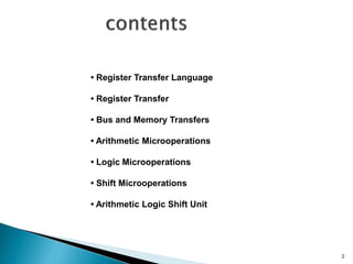
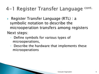
![ Assume that the address of a memory unit is
stored in a register called the Address
Register AR
Lets represent a Data Register with DR, then:
Read: DR ← M[AR]
Write: M[AR] ← DR
Computer Organization 21](https://image.slidesharecdn.com/microoperations-210212051642/85/Micro-operations-21-320.jpg)
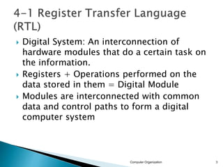
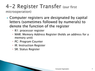
![Computer Organization 22
AR
x12
x0C
x0E
x10
x12
x14
x16
x18
19
34
45
66
0
13
22
R1←M[AR]
R1
100
R1
66
RAM
R1
100](https://image.slidesharecdn.com/microoperations-210212051642/85/Micro-operations-22-320.jpg)


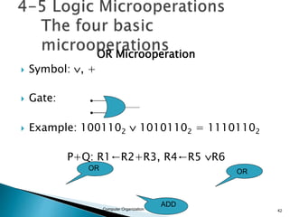
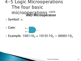
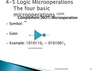
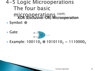


The document discusses register transfer and microoperations in computer organization. It defines register transfer language (RTL) as a symbolic notation used to describe microoperation transfers among registers. It describes different types of microoperations including register transfer, arithmetic, logic, and shift microoperations. It also provides examples of common microoperations like addition, AND, OR, complement, and selective operations.