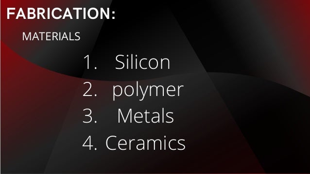
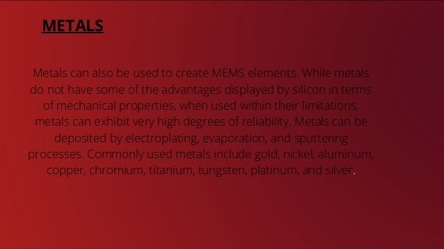
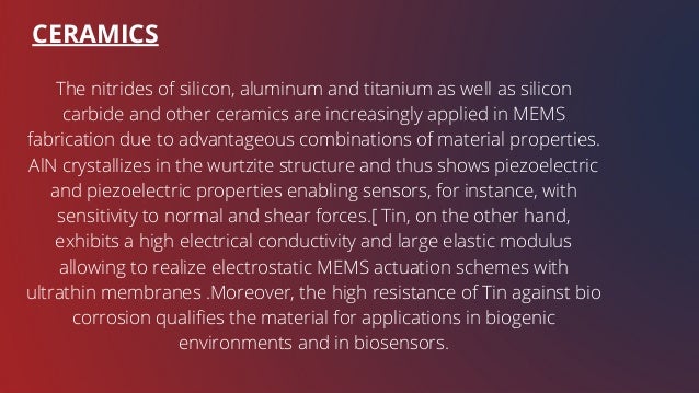
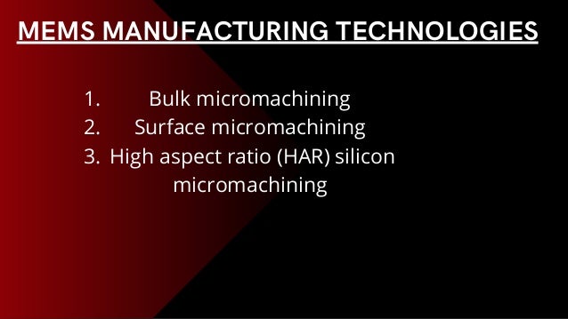
2. Topics Covered
WHAT IS MEMS?
WHAT IS SENSOR
FABRICATION
MEMS MANUFACTURING
TECHNOLOGIES:
Agenda
3. A d e v i c e u s e d t o m e a s u r e a p h y s i c a l q u a n t i t y ( s u c h a s
t e m p e r a t u r e ) a n d c o n v e r t i t i n t o a n e l e c t r o n i c s i g n a l o f
s o m e k i n d ( e . g a v o l t a g e ) , w i t h o u t m o d i f y i n g t h e
e n v i r o n m e n t . A s e n s o r i s a d e v i c e w h i c h r e c e i v e s a n d
r e s p o n d s t o a s i g n a l . A s e n s o r ' s s e n s i t i v i t y i n d i c a t e s h o w
m u c h t h e s e n s o r ' s o u t p u t c h a n g e s w h e n t h e m e a s u r e d
q u a n t i t y c h a n g e s . S e n s o r s a r e u s e d i n e v e r y d a y o b j e c t s s u c h
a s t o u c h - s e n s i t i v e e l e v a t o r b u t t o n s ( t a c t i l e s e n s o r ) a n d
l a m p s w h i c h d i m o r b r i g h t e n b y t o u c h i n g t h e b a s e . T h e r e
a r e a l s o i n n u m e r a b l e a p p l i c a t i o n s f o r s e n s o r s o f w h i c h m o s t
p e o p l e a r e n e v e r a w a r e . A p p l i c a t i o n s i n c l u d e c a r s ,
m a c h i n e s , a e r o s p a c e , m e d i c i n e , m a n u f a c t u r i n g a n d
r o b o t i c s .
WHAT IS SENSOR?
4. Microelectromechanical systems (MEMS) are small integrated devices or systems that combine
electrical and mechanical components. They range in size from the sub micrometer (or sub
micron) level to the millimeter level, and there can be any number, from a few to millions, in a
particular system. MEMS extend the fabrication techniques developed for the integrated circuit
industry to add mechanical elements such as beams, gears, diaphragms, and springs to devices.
These systems can sense, control, and activate mechanical processes on the micro scale, and
function individually or in arrays to generate effects on the macro scale. The micro fabrication
technology enables fabrication of large arrays of devices, which individually perform simple tasks,
but in combination can accomplish complicated functions.MicroElectro-Mechanical Systems, or
MEMS, is a technology that in its most general form can be defined as miniaturized mechanical
and electro-mechanical elements (i.e., devices and structures) that are made using the
techniques of micro fabrication.
WHAT IS MEMS?
6. SILICON
Silicon is the material used to create most integrated circuits used in consumer
electronics in the modern world. The economies of scale, ready availability of cheap
highquality materials and ability to incorporate electronic functionality make silicon
attractive for a wide variety of MEMS applications. Silicon also has significant
advantages engendered through its material properties. In single crystal form, silicon
is an almost perfect Hooke an material, meaning that when it is flexed there is
virtually no hysteresis and hence almost no energy dissipation. As well as making for
highly repeatable motion, this also makes silicon very reliable as it suffers very little
fatigue and can have service lifetimes in the range of billions to trillions of cycles
without breaking
7. POLYMER
Even though the electronics industry provides an economy of scale for the
silicon industry, crystalline silicon is still a complex and relatively expensive
material to produce. Polymers on the other hand can be produced in huge
volumes, with a great variety of material characteristics. MEMS devices can be
made from polymers by processes such as injection molding, embossing or
stereo lithography and are especially well suited to micro fluidic applications
such as disposable blood testing cartridges.
8. 7 out of 7
100%
7 million
METALS
Metals can also be used to create MEMS elements. While metals
do not have some of the advantages displayed by silicon in terms
of mechanical properties, when used within their limitations,
metals can exhibit very high degrees of reliability. Metals can be
deposited by electroplating, evaporation, and sputtering
processes. Commonly used metals include gold, nickel, aluminum,
copper, chromium, titanium, tungsten, platinum, and silver.
9. CERAMICS
The nitrides of silicon, aluminum and titanium as well as silicon
carbide and other ceramics are increasingly applied in MEMS
fabrication due to advantageous combinations of material properties.
AlN crystallizes in the wurtzite structure and thus shows piezoelectric
and piezoelectric properties enabling sensors, for instance, with
sensitivity to normal and shear forces.[ Tin, on the other hand,
exhibits a high electrical conductivity and large elastic modulus
allowing to realize electrostatic MEMS actuation schemes with
ultrathin membranes .Moreover, the high resistance of Tin against bio
corrosion qualifies the material for applications in biogenic
environments and in biosensors.
11. Bulk micromachining
Bulk micromachining is the oldest paradigm of silicon based MEMS. The whole thickness of
a silicon wafer is used for building the micro-mechanical structures. Silicon is machined
using various etching processes. Anodic bonding of glass plates or additional silicon wafers
is used for adding features in the third dimension and for hermetic encapsulation. Bulk
micromachining has been essential in enabling high performance pressure sensors and
accelerometers that have changed the shape of the sensor industry in the 80's and 90's.
The differences between the various sorts of etching procedures. The thin layer visible
between the photo resist and the silicon itself is silicon dioxide (SiO2). It serves as an etch
mask for the Si etch, since its etch rate in most of the acidic etchants is considerably lower
than that of Si, whereas photo resists do not stand up to the strong attack of most of the
etchants. It is either a naturally grown oxide of approximately 20 Å (oxidation of silicon is
nearlyunavoidable when exposed to an atmosphere containing oxygen) or is thermally
grown to a distinctive thickness.
12. SURFACE MICROMACHINING:
In contrast to the bulk micromachining described above, where three-
dimensional structures are etched into the substrate wafer, surface
micromachining consists of building them by layering thin films of new
material onto the surface of the substrate. Usually, sacrificial spacer layers
are used to create freestanding structures like air-bridges; after
depositing such a sacrificial layer and patterning it using micro
lithographic steps described above, the material for the final structure is
deposited. Afterwards, the spacer layer is removed by an appropriate
etchant, freeing the desired structure.
13. HIGH ASPECT RATIO (HAR) SILICON MICROMACHINING:
Both bulk and surface silicon micromachining are used in the industrial production of sensors, ink-jet
nozzles, and other devices. But in many cases the distinction between these two has diminished. A
new etching technology, deep reactive-ion etching, has made it possible to combine good
performance typical of bulk micromachining with comb structures and in-plane operation typical of
surface micromachining. While it is common in surface micromachining to have structural layer
thickness in the range of 2 µm, in HAR silicon micromachining the thickness can be from 10 to 100
µm. The materials commonly used in HAR silicon micromachining are thick polycrystalline silicon,
known as epi-poly, and bonded silicon-on-insulator (SOI) wafers although processes for bulk silicon
wafer also have been created (SCREAM). Bonding a second wafer by glass frit bonding, anodic
bonding or alloy bonding is used to protect the MEMS structures. Integrated circuits are typically not
combined with HAR silicon micromachining. The consensus of the industry at the moment seems to
be that the flexibility and reduced process complexity obtained by having the two functions
separated far outweighs the small penalty in packaging. A comparison of different high-aspect-ratio
microstructure technologies can be found in the HARMST article.