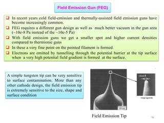
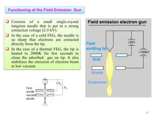
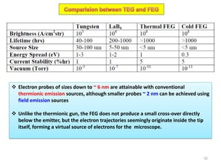
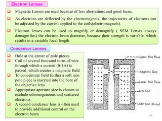
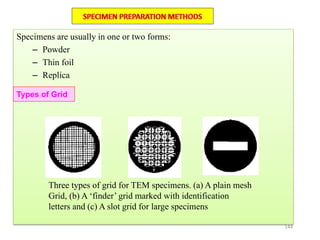
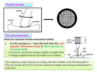
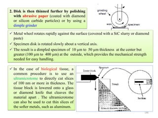
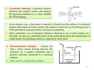
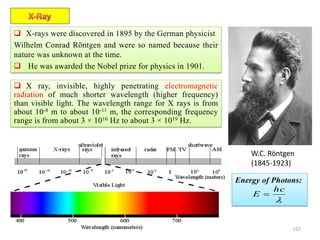
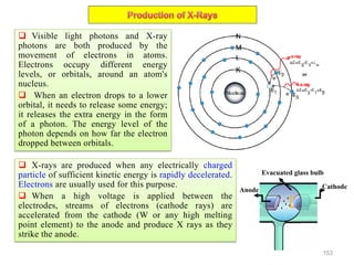
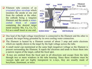
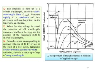
Downloaded 831 times
![Crystallographic Directions
A crystallographic direction is defined as a line between 2 points, or a vector.
The following steps are utilized in the determination of the 3 directional indices:
A vector of convenient length is positioned such that it passes through the origin of
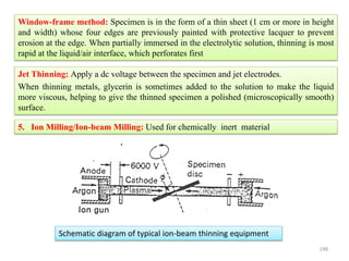
the coordinate system.
Any vector may be translated throughout the crystal lattice without alteration, if
parallelism in maintained.
The length of the vector projection on each of the 3 axes is determined; these are
measured in terms of the unit cell dimensions a, b, and c.
These 3 numbers are multiplied or divided by a common factor to reduce them to the
smallest integer values.
The 3 indices (not separated by commas) are enclosed in square brackets: [uvw]
where u, v, and w integers correspond to the reduced projection along the x, y, and z
axes, respectively.
A vector r passing from the origin to a lattice
point can be written as:
r = r1 a + r2 b + r3 c Where, a, b, c → basic
vectors
Note their length is not 1 unit! (like for the basis
vectors of a coordinate axis).
11](https://image.slidesharecdn.com/materialscharacterizationtechnique-160429090201/85/Materials-Characterization-Technique-Lecture-Notes-11-320.jpg)
![[010]
[100]
[001]
[110]
[101]
[011]
[110] [111]
Important directions in 3D represented by Miller Indices (cubic lattice)
Face diagonal
Body diagonal
X
Y
Z
Memorize these
116](https://image.slidesharecdn.com/materialscharacterizationtechnique-160429090201/85/Materials-Characterization-Technique-Lecture-Notes-12-320.jpg)
![[+ + -] [+ - -]
[+ - +]
[- - +][- + +]
[+ + +]
[- - -][- + -]
If you have confusion while selecting origin in negative indices refer this figure
Possible coordinates in 3D
X
Y
Z
117](https://image.slidesharecdn.com/materialscharacterizationtechnique-160429090201/85/Materials-Characterization-Technique-Lecture-Notes-13-320.jpg)
![Family of directions
Index Members in family for cubic lattice Number
<100> 3 x 2 = 6
<110>
6 x 2 =
12
<111> 4 x 2 = 8
Symbol
Alternate
symbol
[ ] → Particular direction
< > [[ ]] → Family of directions
[100],[100],[010],[010],[001],[001]
[110],[110],[110],[110],[101],[101],[101],[101],[011],[011],[011],[011]
[111],[111],[111],[111],[111],[111],[111],[111]
the ‘negatives’
(opposite direction)
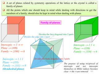
A set of directions related by symmetry operations of the lattice or the crystal is called a
family of directions
A family of directions is represented (Miller Index notation) as: <u v w>
118](https://image.slidesharecdn.com/materialscharacterizationtechnique-160429090201/85/Materials-Characterization-Technique-Lecture-Notes-14-320.jpg)
![• Trace a path along the basis vectors as required by the direction. In the current example move
1unit along a1, 1unit along a2 and 2 units along a3.
• Directions are projected onto the basis vectors to determine the components and hence the Miller-
Bravais indices can be determined as in the table.
[1120]Drawing the direction
Hexagonal crystals → Miller-Bravais Indices : DIRECTIONS
Drawing the [10 0] direction1
129](https://image.slidesharecdn.com/materialscharacterizationtechnique-160429090201/85/Materials-Characterization-Technique-Lecture-Notes-22-320.jpg)
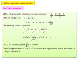
![ Unknown direction → [uvw]
Unknown plane → (hkl)
Double digit indices should be separated by commas → (12,22,3)
In cubic lattices/crystals [hkl] (hkl)
2 2 2
cubic lattice
hkl
a
d
h k l
Points about planes and directions
Interplanar spacing (dhkl) in cubic
lattice (& crystals)
Symbol
Alternate
symbols
Direction
[ ] [uvw] → Particular direction
< > <uvw> [[ ]] → Family of directions
Plane
( ) (hkl) → Particular plane
{ } {hkl} (( )) → Family of planes
122](https://image.slidesharecdn.com/materialscharacterizationtechnique-160429090201/85/Materials-Characterization-Technique-Lecture-Notes-23-320.jpg)


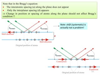
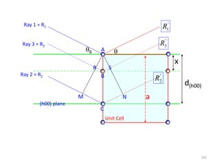
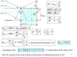
![Note: shift is actually not a problem! Why is ‘systematic’ shift not a problem?
n AY YB [180 ( )] ( )AY XY Cos XY Cos
( )YB XY Cos
[ ( ) ( )] [2 ]n AY YB XY Cos Cos XY Sin Sin
( )
d
Sin
XY
[2 ] 2
d
n Sin Sin d Sin
Sin
2n d Sin
172](https://image.slidesharecdn.com/materialscharacterizationtechnique-160429090201/85/Materials-Characterization-Technique-Lecture-Notes-172-320.jpg)
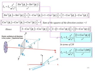
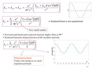
![0
0.2
0.4
0.6
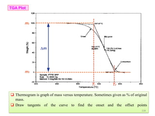
0.8
1
0 30 60 90 120 150 180
2t
[Cos(2t)]^2
In general P could lie anywhere in 3D
space.
For the specific case of Bragg scattering:
The incident direction IO
The diffracted beam direction OP
The trace of the scattering plane BB’
Are all coplanar OP is constrained to be
on the xz plane
x
z
r
P
2
2
2
42
4
0
2
r
Cos
cm
e
II
186](https://image.slidesharecdn.com/materialscharacterizationtechnique-160429090201/85/Materials-Characterization-Technique-Lecture-Notes-186-320.jpg)
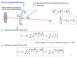
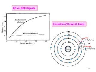
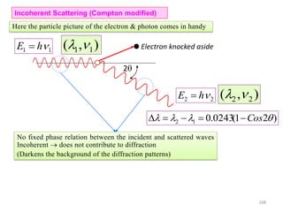
![B Scattering by an Atom
Scattering by an atom [Atomic number, (path difference suffered by scattering from
each e−, )]
Scattering by an atom [Z, (, )] Angle of scattering leads to path differences
In the forward direction all scattered waves are in phase
electronanbyscatteredwaveofAmplitude
atomanbyscatteredwaveofAmplitude
FactorScatteringAtomicf
f→
)(Sin
(Å−1) →
0.2 0.4 0.6 0.8 1.0
10
20
30
Schematic
)(Sin
Coherent
scattering
Incoherent
(Compton)
scattering
Z
Sin() /
189](https://image.slidesharecdn.com/materialscharacterizationtechnique-160429090201/85/Materials-Characterization-Technique-Lecture-Notes-189-320.jpg)
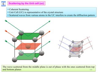
![ If atom B is different from atom A the amplitudes must be weighed by the respective
atomic scattering factors (f)
The resultant amplitude of all the waves scattered by all the atoms in the UC gives the
scattering factor for the unit cell
The unit cell scattering factor is called the Structure Factor (F)
Scattering by an unit cell = f(position of the atoms, atomic scattering factors)
electronanbyscatteredwaveofAmplitude
ucinatomsallbyscatteredwaveofAmplitude
FactorStructureF
[2 ( )]i i h x k y l z
E Ae fe
2 ( )h x k y l z
In complex notation
2
FI
[2 ( )]
1 1
j j j j
n n
i i h x k y l zhkl
n j j
j j
F f e f e
Structure factor is independent of the shape and size of the unit cell
For n atoms in the UC
If the UC distorts so do the planes in it!!
193](https://image.slidesharecdn.com/materialscharacterizationtechnique-160429090201/85/Materials-Characterization-Technique-Lecture-Notes-193-320.jpg)
![nni
e )1(
)(
2
Cos
ee ii
Structure factor calculations
A Atom at (0,0,0) and equivalent positions
[2 ( )]j j j ji i h x k y l z
j jF f e f e
[2 ( 0 0 0)] 0i h k l
F f e f e f
22
fF F is independent of the scattering plane (h k l)
nini
ee
Simple Cubic
1)(
inodd
e
1)(
ineven
e
194](https://image.slidesharecdn.com/materialscharacterizationtechnique-160429090201/85/Materials-Characterization-Technique-Lecture-Notes-194-320.jpg)
![B Atom at (0,0,0) & (½, ½, 0) and equivalent positions
[2 ( )]j j j ji i h x k y l z
j jF f e f e
1 1
[2 ( 0)]
[2 ( 0 0 0)] 2 2
[ 2 ( )]
0 ( )2
[1 ]
i h k l
i h k l
h k
i
i h k
F f e f e
f e f e f e
F is independent of the ‘l’index
C- centred Orthorhombic
Real
]1[ )( khi
efF
fF 2
0F
22
4 fF
02
F
e.g. (001), (110), (112); (021), (022), (023)
e.g. (100), (101), (102); (031), (032), (033)
195](https://image.slidesharecdn.com/materialscharacterizationtechnique-160429090201/85/Materials-Characterization-Technique-Lecture-Notes-195-320.jpg)
![C Atom at (0,0,0) & (½, ½, ½) and equivalent positions
[2 ( )]j j j ji i h x k y l z
j jF f e f e
1 1 1
[2 ( )]
[2 ( 0 0 0)] 2 2 2
[ 2 ( )]
0 ( )2
[1 ]
i h k l
i h k l
h k l
i
i h k l
F f e f e
f e f e f e
Body centred
Orthorhombic
Real
]1[ )( lkhi
efF
fF 2
0F
22
4 fF
02
F
e.g. (110), (200), (211); (220), (022), (310)
e.g. (100), (001), (111); (210), (032), (133)
196](https://image.slidesharecdn.com/materialscharacterizationtechnique-160429090201/85/Materials-Characterization-Technique-Lecture-Notes-196-320.jpg)
![D Atom at (0,0,0) & (½, ½, 0) and equivalent positions
[2 ( )]j j j ji i h x k y l z
j jF f e f e
]1[ )()()(
)]
2
(2[)]
2
(2[)]
2
(2[
)]0(2[
hlilkikhi
hl
i
lk
i
kh
i
i
eeef
eeeefF
Face Centred Cubic
Real
fF 4
0F
22
16 fF
02
F
(h, k, l) unmixed
(h, k, l) mixed
e.g. (111), (200), (220), (333), (420)
e.g. (100), (211); (210), (032), (033)
(½, ½, 0), (½, 0, ½), (0, ½, ½)
]1[ )()()( hlilkikhi
eeefF
Two odd and one even (e.g. 112); two even and one odd (e.g. 122) 197](https://image.slidesharecdn.com/materialscharacterizationtechnique-160429090201/85/Materials-Characterization-Technique-Lecture-Notes-197-320.jpg)
![Mixed indices CASE h k l
A o o e
B o e e
( ) ( ) ( )
CASE A : [1 ] [1 1 1 1] 0i e i o i o
e e e
( ) ( ) ( )
CASE B: [1 ] [1 1 1 1] 0i o i e i o
e e e
0F 02
F(h, k, l) mixed e.g. (100), (211); (210), (032), (033)
Mixed indices Two odd and one even (e.g. 112); two even and one odd (e.g. 122)
Unmixed indices CASE h k l
A o o o
B e e e
Unmixed indices
fF 4 22
16 fF (h, k, l) unmixed
e.g. (111), (200), (220), (333), (420)
All odd (e.g. 111); all even (e.g. 222)
( ) ( ) ( )
CASE A : [1 ] [1 1 1 1] 4i e i e i e
e e e
( ) ( ) ( )
CASE B: [1 ] [1 1 1 1] 4i e i e i e
e e e
198](https://image.slidesharecdn.com/materialscharacterizationtechnique-160429090201/85/Materials-Characterization-Technique-Lecture-Notes-198-320.jpg)
![E
Na+ at (0,0,0) + Face Centering Translations (½, ½, 0), (½, 0, ½), (0, ½, ½)
Cl− at (½, 0, 0) + FCT (0, ½, 0), (0, 0, ½), (½, ½, ½)
)]
2
(2[)]
2
(2[)]
2
(2[)]
2
(2[
)]
2
(2[)]
2
(2[)]
2
(2[
)]0(2[
lkh
i
l
i
k
i
h
i
Cl
hl
i
lk
i
kh
i
i
Na
eeeef
eeeefF
][
]1[
)()()()(
)()()(
lkhilikihi
Cl
hlilkikhi
Na
eeeef
eeefF
]1[
]1[
)()()()(
)()()(
khihlilkilkhi
Cl
hlilkikhi
Na
eeeef
eeefF
]1][[ )()()()( hlilkikhilkhi
ClNa
eeeeffF
NaCl:
Face Centred Cubic
199](https://image.slidesharecdn.com/materialscharacterizationtechnique-160429090201/85/Materials-Characterization-Technique-Lecture-Notes-199-320.jpg)
![]1][[ )()()()( hlilkikhilkhi
ClNa
eeeeffF
Zero for mixed indices
Mixed indices CASE h k l
A o o e
B o e e
]2][1[ TermTermF
0]1111[]1[2:ACASE )()()(
oioiei
eeeTerm
0]1111[]1[2:BCASE )()()(
oieioi
eeeTerm
0F 02
F(h, k, l) mixed e.g. (100), (211); (210), (032), (033)
Mixed indices
200](https://image.slidesharecdn.com/materialscharacterizationtechnique-160429090201/85/Materials-Characterization-Technique-Lecture-Notes-200-320.jpg)
![(h, k, l) unmixed ][4 )( lkhi
ClNa
effF
][4 ClNa
ffF If (h + k + l) is even
22
][16 ClNa
ffF
][4 ClNa
ffF If (h + k + l) is odd
22
][16 ClNa
ffF
e.g. (111), (222); (133), (244)
e.g. (222),(244)
e.g. (111), (133)
Unmixed indices CASE h k l
A o o o
B e e e
4]1111[]1[2:ACASE )()()(
eieiei
eeeTerm
4]1111[]1[2:BCASE )()()(
eieiei
eeeTerm
Unmixed indices
201](https://image.slidesharecdn.com/materialscharacterizationtechnique-160429090201/85/Materials-Characterization-Technique-Lecture-Notes-201-320.jpg)
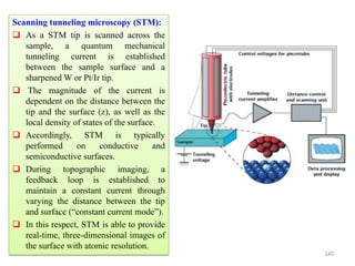
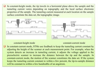
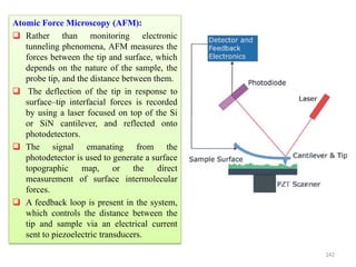
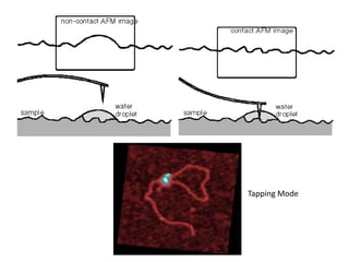

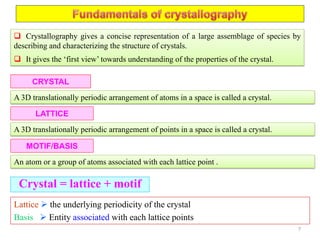
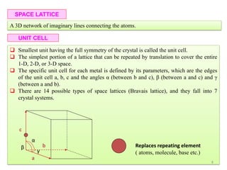
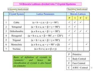
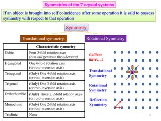
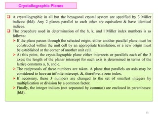
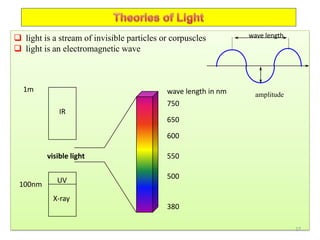
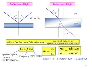
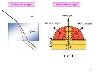
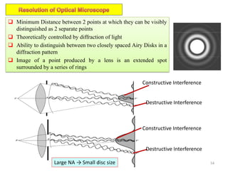
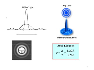
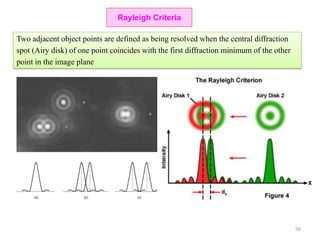
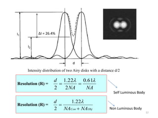
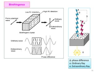
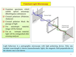
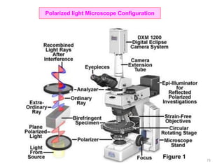
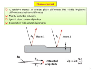
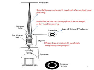
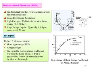
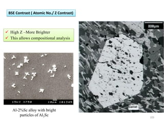
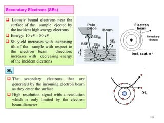
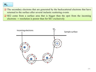
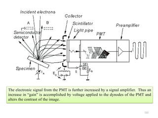
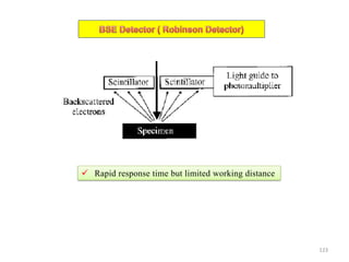
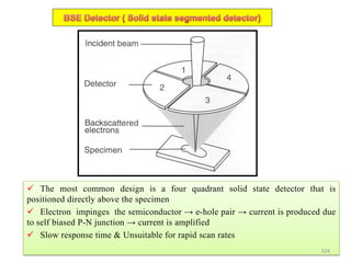
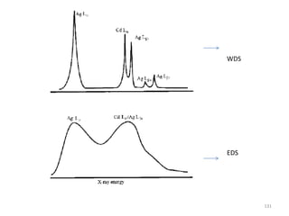
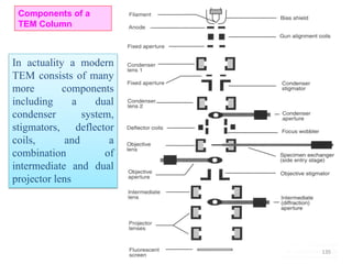
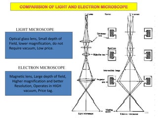
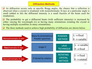
The document contains lecture notes on materials characterization, detailing essential topics such as optical microscopy, scanning electron microscopy, and X-ray diffraction. It emphasizes the importance of accurately measuring the physical and chemical properties of materials for structure-property correlation. Additionally, it includes information on crystallography, crystal structure definitions, and various microscopy techniques.


