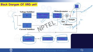
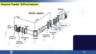
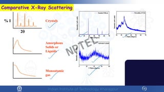
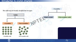
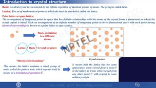
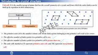
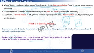
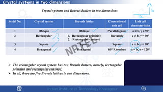
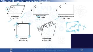
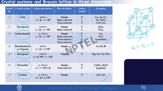
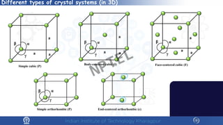
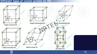
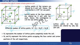
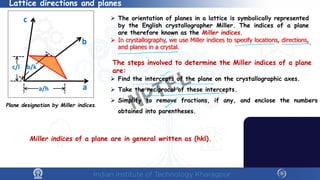
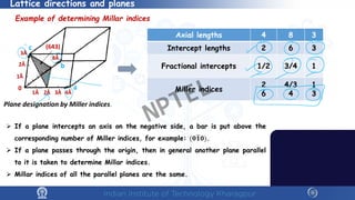
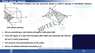
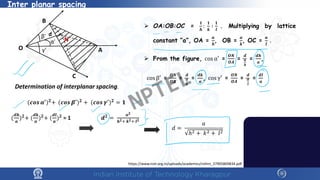
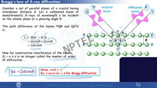
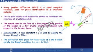
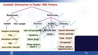
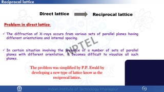
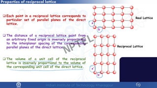
The document covers the synthesis protocols and crystal structures of materials, focusing on different types of lattices, unit cells, and crystal systems, including bravais lattices. It explains concepts like miller indices, inter-planar spacing, and x-ray diffraction for analyzing crystal structures. The lecture emphasizes the significance of symmetries within crystal structures and introduces techniques for visualizing crystalline states using x-ray diffraction methods.


![In Miller indices, the brackets and commas matter a lot!
Notation Representation
(h,k,l) Point
[hkl] Direction
<hkl> Family of directions
(hkl) Plane
{hkl} Family of planes
Negative weights can be represented with a bar over the relevant number
NPTEL](https://image.slidesharecdn.com/lm-week3-240831073155-f340f5b9/85/PHYSICS-OF-FUNCTIONAL-MATERIAL-AND-DEVICESpdf-22-320.jpg)


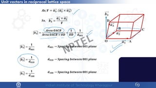
![Unit vectors in reciprocal lattice space
Unit vectors in real space:
𝒂𝒂𝟏𝟏 𝒂𝒂𝟐𝟐 𝒂𝒂𝟑𝟑
Unit vectors in reciprocal lattice space:
𝒃𝒃𝟏𝟏 𝒃𝒃𝟐𝟐 𝒃𝒃𝟑𝟑
𝒃𝒃𝟏𝟏 =
𝒂𝒂𝟐𝟐 × 𝒂𝒂𝟑𝟑
𝒂𝒂𝟏𝟏. (𝒂𝒂𝟐𝟐 × 𝒂𝒂𝟑𝟑)
𝒃𝒃𝟐𝟐 =
𝒂𝒂𝟑𝟑 × 𝒂𝒂𝟏𝟏
𝒂𝒂𝟏𝟏. (𝒂𝒂𝟐𝟐 × 𝒂𝒂𝟑𝟑)
𝒃𝒃𝟑𝟑 =
𝒂𝒂𝟏𝟏 × 𝒂𝒂𝟐𝟐
𝒂𝒂𝟏𝟏. (𝒂𝒂𝟐𝟐 × 𝒂𝒂𝟑𝟑)
Unit vectors relation between real space and reciprocal lattice space :
𝒂𝒂𝟏𝟏. 𝒂𝒂𝟐𝟐 × 𝒂𝒂𝟑𝟑 = 𝑽𝑽, 𝒗𝒗𝒗𝒗𝒗𝒗𝒗𝒗𝒗𝒗𝒗𝒗 𝒐𝒐𝒐𝒐 𝒕𝒕𝒕𝒕𝒕𝒕 𝒖𝒖𝒖𝒖𝒖𝒖𝒖𝒖 𝒄𝒄𝒄𝒄𝒄𝒄𝒄𝒄
𝒃𝒃𝟑𝟑 =
𝒂𝒂𝟏𝟏 × 𝒂𝒂𝟐𝟐
𝑽𝑽
𝑺𝑺𝑺𝑺, 𝒃𝒃𝟑𝟑 � 𝒂𝒂𝟐𝟐 = 𝟎𝟎
𝒃𝒃𝟑𝟑 � 𝒂𝒂𝟏𝟏 = 𝟎𝟎
𝒃𝒃𝟑𝟑 � 𝒂𝒂𝟑𝟑 = 𝟏𝟏
𝒃𝒃𝒊𝒊 � 𝒂𝒂𝒋𝒋 = 𝟎𝟎 [𝒊𝒊 ≠ 𝒋𝒋]
𝒃𝒃𝒊𝒊 � 𝒂𝒂𝒋𝒋 = 𝟏𝟏 [𝒊𝒊 = 𝒋𝒋]
𝒃𝒃𝟑𝟑 𝒊𝒊𝒊𝒊 𝒑𝒑𝒑𝒑𝒑𝒑𝒑𝒑𝒑𝒑𝒑𝒑𝒑𝒑𝒑𝒑𝒑𝒑𝒑𝒑𝒑𝒑𝒑𝒑𝒑𝒑 𝒕𝒕𝒕𝒕 𝒂𝒂𝟏𝟏 × 𝒂𝒂𝟐𝟐 𝒑𝒑𝒑𝒑𝒑𝒑𝒑𝒑𝒑𝒑
NPTEL](https://image.slidesharecdn.com/lm-week3-240831073155-f340f5b9/85/PHYSICS-OF-FUNCTIONAL-MATERIAL-AND-DEVICESpdf-41-320.jpg)
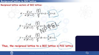
![Reciprocal lattice to BCC lattice
The primitive translation vectors of a body-centred
cubic lattice:
𝒂𝒂′ =
𝒂𝒂
𝟐𝟐
( ̂
𝒊𝒊 + ̂
𝒋𝒋 − �
𝒌𝒌) 𝒃𝒃′
=
𝒂𝒂
𝟐𝟐
(− ̂
𝒊𝒊 + ̂
𝒋𝒋 + �
𝒌𝒌) 𝒄𝒄′
=
𝒂𝒂
𝟐𝟐
( ̂
𝒊𝒊 − ̂
𝒋𝒋 + �
𝒌𝒌)
The volume of the primitive cell : 𝑽𝑽 = 𝒂𝒂′
. (𝒃𝒃′ × 𝒄𝒄′)
=
𝒂𝒂
𝟐𝟐
̂
𝒊𝒊 + ̂
𝒋𝒋 − �
𝒌𝒌 . [
𝒂𝒂𝟐𝟐
𝟒𝟒
(− ̂
𝒊𝒊 + ̂
𝒋𝒋 + �
𝒌𝒌) × ( ̂
𝒊𝒊 − ̂
𝒋𝒋 + �
𝒌𝒌)]
=
𝒂𝒂
𝟐𝟐
̂
𝒊𝒊 + ̂
𝒋𝒋 − �
𝒌𝒌 .
𝒂𝒂𝟐𝟐
𝟐𝟐
( ̂
𝒊𝒊 + ̂
𝒋𝒋)
=
𝒂𝒂𝟑𝟑
𝟐𝟐
NPTEL](https://image.slidesharecdn.com/lm-week3-240831073155-f340f5b9/85/PHYSICS-OF-FUNCTIONAL-MATERIAL-AND-DEVICESpdf-46-320.jpg)
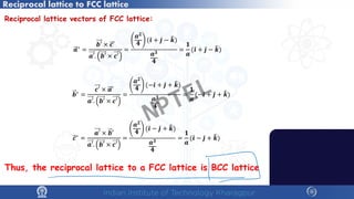
![Reciprocal lattice to FCC lattice
The primitive translation vectors of a face-centred cubic lattice:
𝒂𝒂′ =
𝒂𝒂
𝟐𝟐
( ̂
𝒊𝒊 + ̂
𝒋𝒋) 𝒃𝒃′
=
𝒂𝒂
𝟐𝟐
( ̂
𝒋𝒋 + �
𝒌𝒌) 𝒄𝒄′ =
𝒂𝒂
𝟐𝟐
(�
𝒌𝒌 + ̂
𝒊𝒊)
The volume of the primitive cell : 𝑽𝑽 = 𝒂𝒂′
. (𝒃𝒃′ × 𝒄𝒄′)
=
𝒂𝒂
𝟐𝟐
̂
𝒊𝒊 + ̂
𝒋𝒋 . [
𝒂𝒂𝟐𝟐
𝟒𝟒
( ̂
𝒋𝒋 + �
𝒌𝒌) × (�
𝒌𝒌 + ̂
𝒊𝒊)]
=
𝒂𝒂
𝟐𝟐
̂
𝒊𝒊 + ̂
𝒋𝒋 .
𝒂𝒂𝟐𝟐
𝟒𝟒
( ̂
𝒊𝒊 + ̂
𝒋𝒋 − �
𝒌𝒌)
=
𝒂𝒂𝟑𝟑
𝟒𝟒
NPTEL](https://image.slidesharecdn.com/lm-week3-240831073155-f340f5b9/85/PHYSICS-OF-FUNCTIONAL-MATERIAL-AND-DEVICESpdf-48-320.jpg)
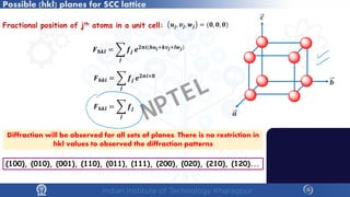
![(110), (200), (211), (220).....
Possible (hkl) planes for BCC lattice
Fractional position of jth atoms in a unit cell:
𝑭𝑭𝒉𝒉𝒉𝒉𝒉𝒉 = �
𝒋𝒋
𝒇𝒇𝒋𝒋 𝒆𝒆𝟐𝟐𝝅𝝅𝒊𝒊(𝒉𝒉𝒖𝒖𝒋𝒋+𝒌𝒌𝒗𝒗𝒋𝒋+𝒍𝒍𝒘𝒘𝒋𝒋)
𝒖𝒖𝒋𝒋, 𝒗𝒗𝒋𝒋, 𝒘𝒘𝒋𝒋 = 𝟎𝟎, 𝟎𝟎, 𝟎𝟎 , (
𝟏𝟏
𝟐𝟐
,
𝟏𝟏
𝟐𝟐
,
𝟏𝟏
𝟐𝟐
)
𝑭𝑭𝒉𝒉𝒉𝒉𝒉𝒉 = �
𝒋𝒋
𝒇𝒇𝒋𝒋 [𝒆𝒆𝟐𝟐𝝅𝝅𝒊𝒊×𝟎𝟎+𝒆𝒆𝝅𝝅𝝅𝝅(𝒉𝒉+𝒌𝒌+𝒍𝒍)]
𝑭𝑭𝒉𝒉𝒉𝒉𝒉𝒉 = �
𝒋𝒋
𝒇𝒇𝒋𝒋 [𝟏𝟏 + 𝒆𝒆𝝅𝝅𝝅𝝅(𝒉𝒉+𝒌𝒌+𝒍𝒍)
]
Diffraction will be observed for particular sets of planes for which
(h+k+l)=even
(100), (111), (120), (122)...
Diffraction pattern will be observed
No diffraction pattern will be observed
𝒂𝒂
𝒄𝒄
𝒃𝒃
NPTEL](https://image.slidesharecdn.com/lm-week3-240831073155-f340f5b9/85/PHYSICS-OF-FUNCTIONAL-MATERIAL-AND-DEVICESpdf-53-320.jpg)
![Possible (hkl) planes for FCC lattice
Fractional position of jth atoms in a unit cell:
𝑭𝑭𝒉𝒉𝒉𝒉𝒉𝒉 = �
𝒋𝒋
𝒇𝒇𝒋𝒋 𝒆𝒆𝟐𝟐𝝅𝝅𝒊𝒊(𝒉𝒉𝒖𝒖𝒋𝒋+𝒌𝒌𝒗𝒗𝒋𝒋+𝒍𝒍𝒘𝒘𝒋𝒋)
𝒖𝒖𝒋𝒋, 𝒗𝒗𝒋𝒋, 𝒘𝒘𝒋𝒋 = 𝟎𝟎, 𝟎𝟎, 𝟎𝟎 ,
𝟏𝟏
𝟐𝟐
,
𝟏𝟏
𝟐𝟐
, 𝟎𝟎 ,
𝟏𝟏
𝟐𝟐
, 𝟎𝟎,
𝟏𝟏
𝟐𝟐
, (𝟎𝟎,
𝟏𝟏
𝟐𝟐
,
𝟏𝟏
𝟐𝟐
)
𝑭𝑭𝒉𝒉𝒉𝒉𝒉𝒉 = �
𝒋𝒋
𝒇𝒇𝒋𝒋 [𝒆𝒆𝟐𝟐𝝅𝝅𝒊𝒊×𝟎𝟎
+𝒆𝒆𝝅𝝅𝝅𝝅(
𝒉𝒉
𝟐𝟐+
𝒌𝒌
𝟐𝟐+𝟎𝟎)
+ 𝒆𝒆𝝅𝝅𝝅𝝅(
𝒉𝒉
𝟐𝟐+𝟎𝟎+
𝒍𝒍
𝟎𝟎)
+ 𝒆𝒆𝝅𝝅𝝅𝝅(𝟎𝟎+
𝒌𝒌
𝟐𝟐+
𝒍𝒍
𝟐𝟐)
]
𝑭𝑭𝒉𝒉𝒉𝒉𝒉𝒉 = �
𝒋𝒋
𝒇𝒇𝒋𝒋 [𝟏𝟏 + 𝒆𝒆𝝅𝝅𝝅𝝅 𝒉𝒉+𝒌𝒌 + 𝒆𝒆𝝅𝝅𝝅𝝅(𝒉𝒉+𝒍𝒍) + 𝒆𝒆𝝅𝝅𝝅𝝅(𝒌𝒌+𝒍𝒍)]
Diffraction will be observed for particular sets of planes for which h,
k, and l is unmixed
(100), (120), (122), (311).....
Diffraction pattern will be observed
No diffraction pattern will be observed
(111), (200), (220), (311).....
𝒂𝒂
𝒄𝒄
𝒃𝒃
NPTEL](https://image.slidesharecdn.com/lm-week3-240831073155-f340f5b9/85/PHYSICS-OF-FUNCTIONAL-MATERIAL-AND-DEVICESpdf-54-320.jpg)