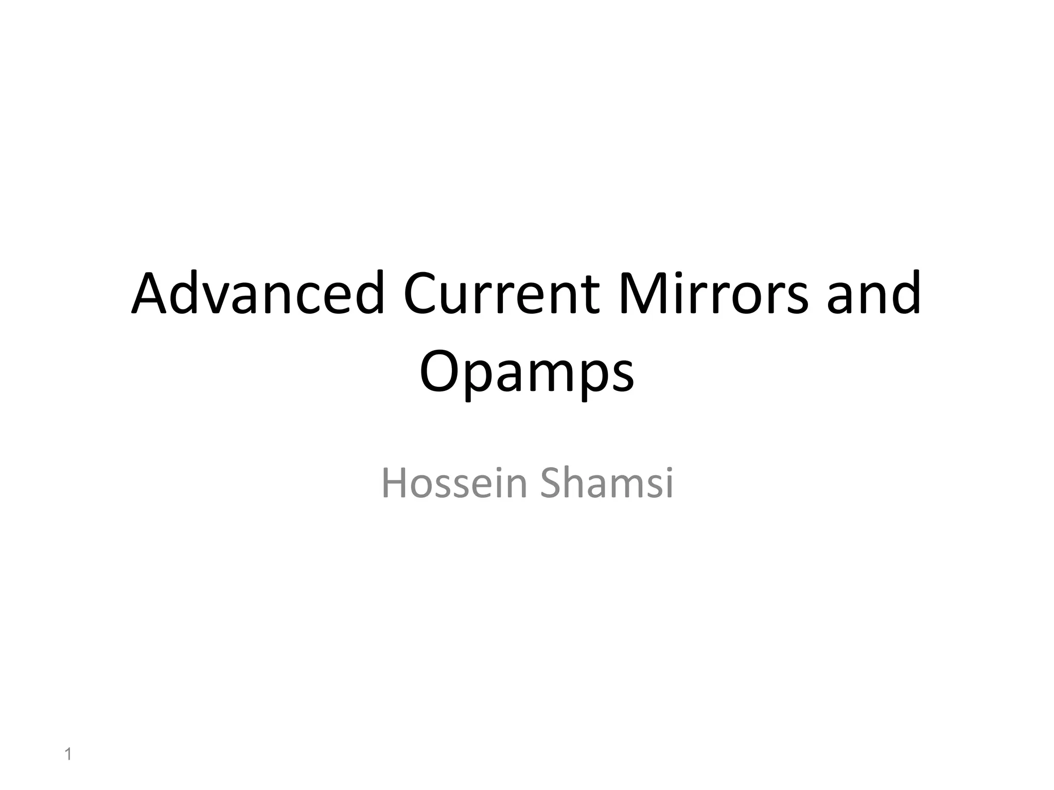
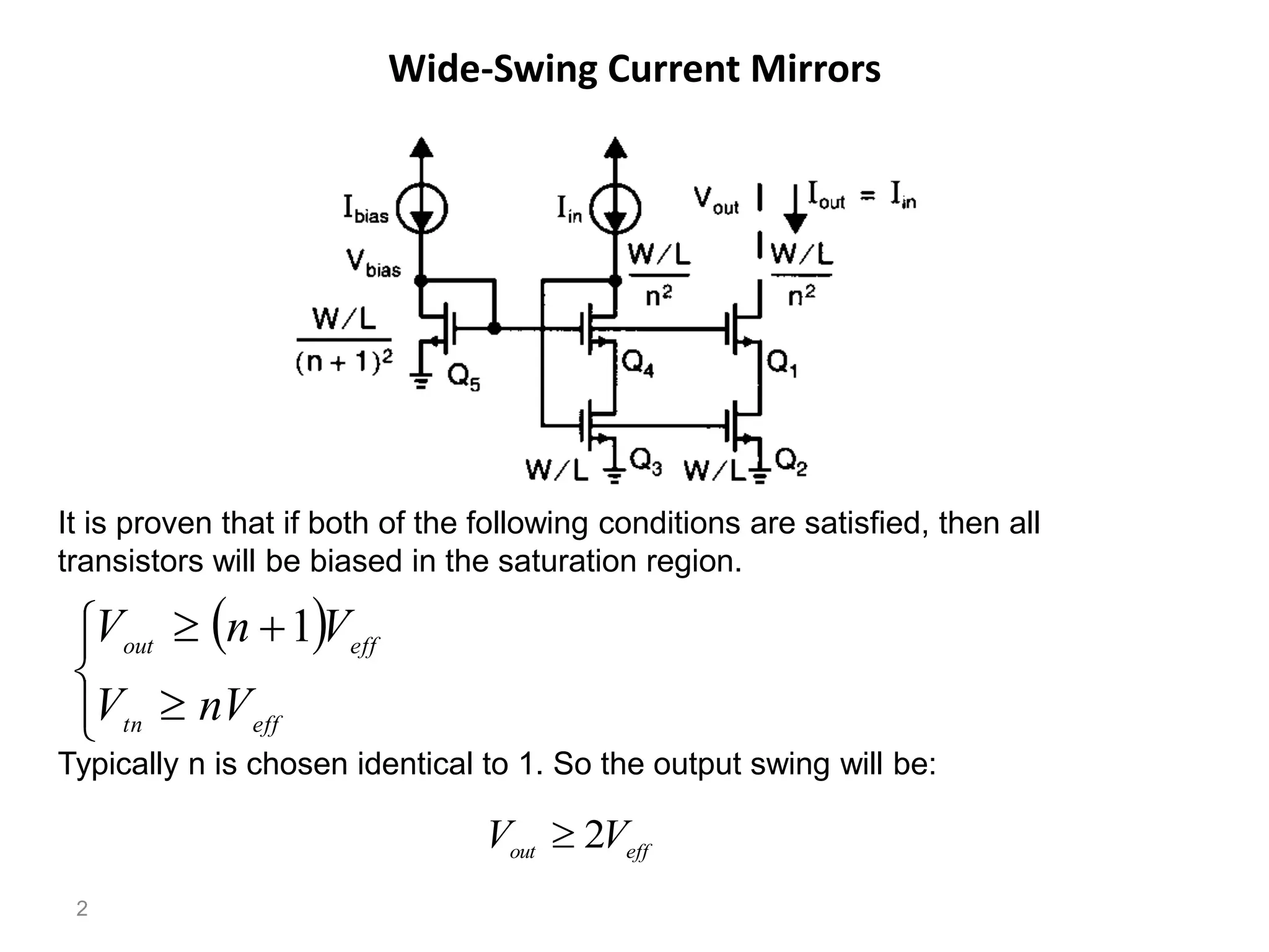
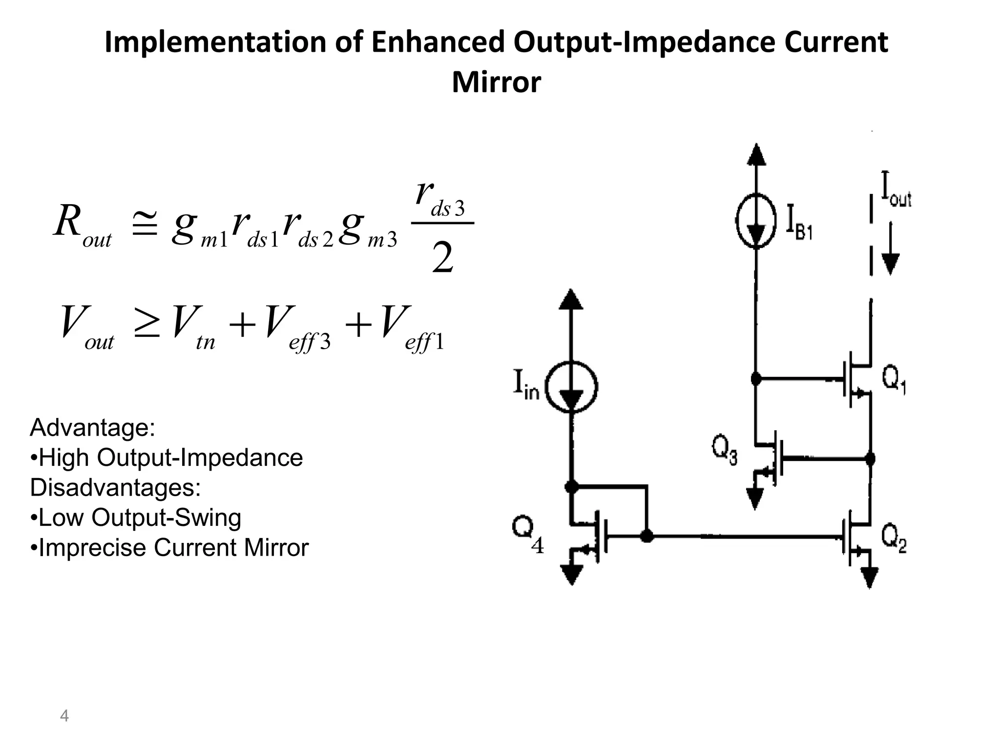
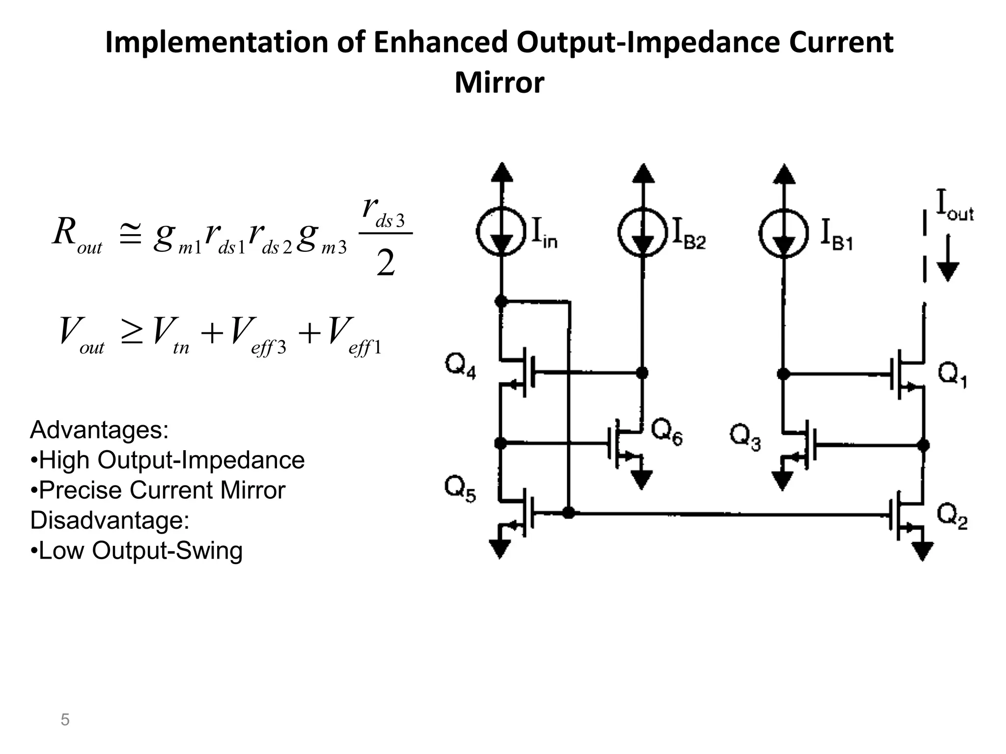
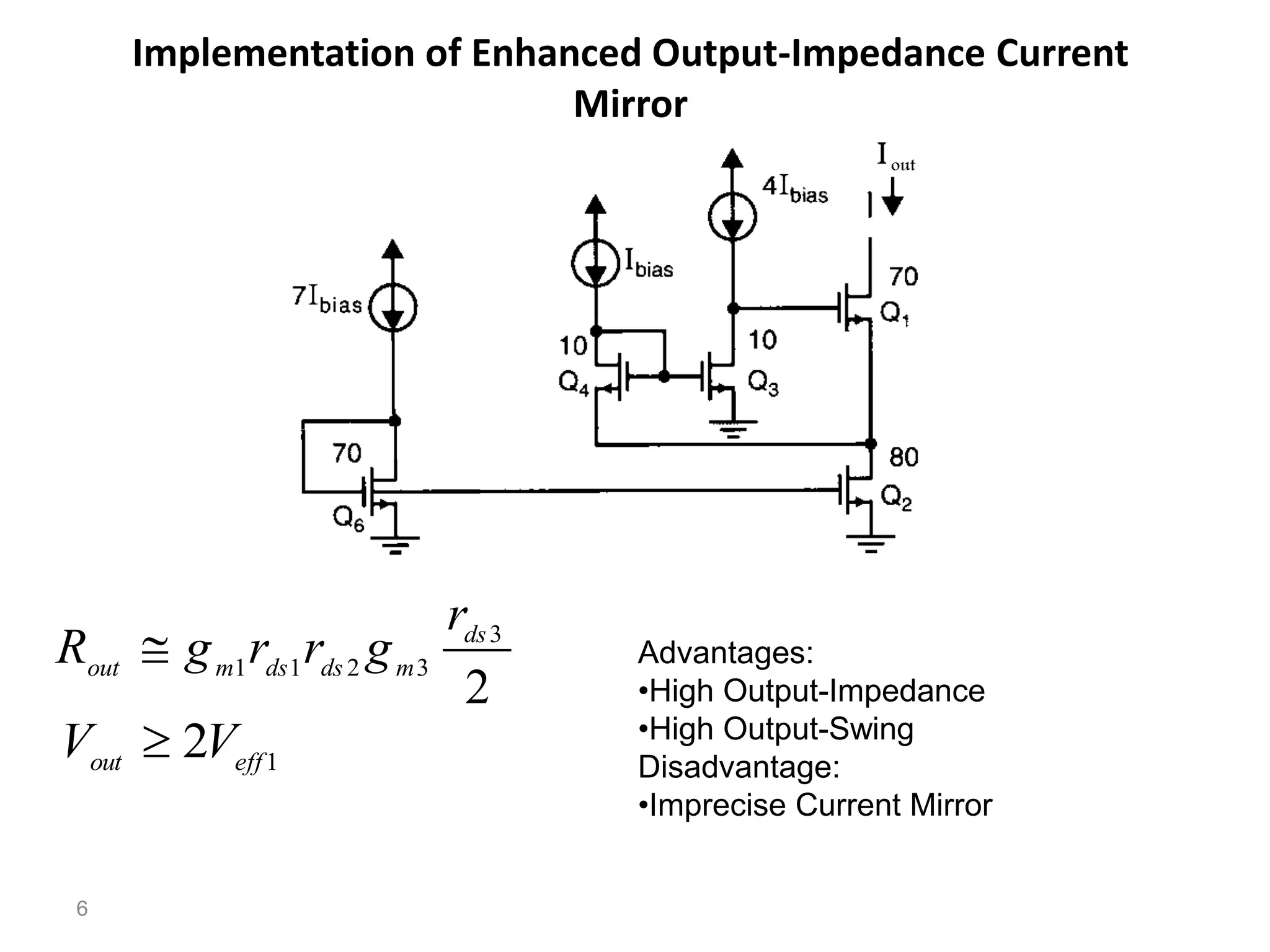
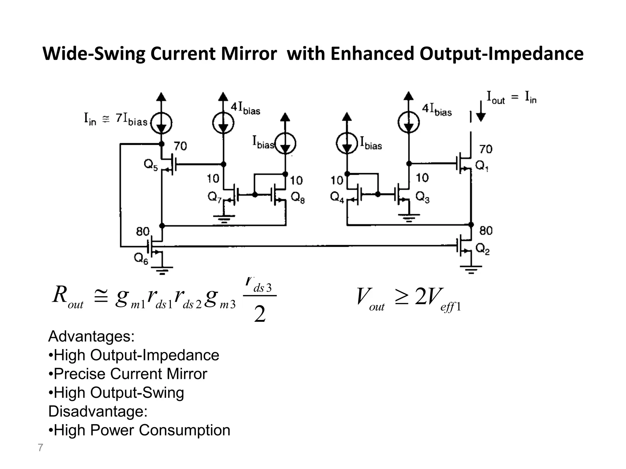
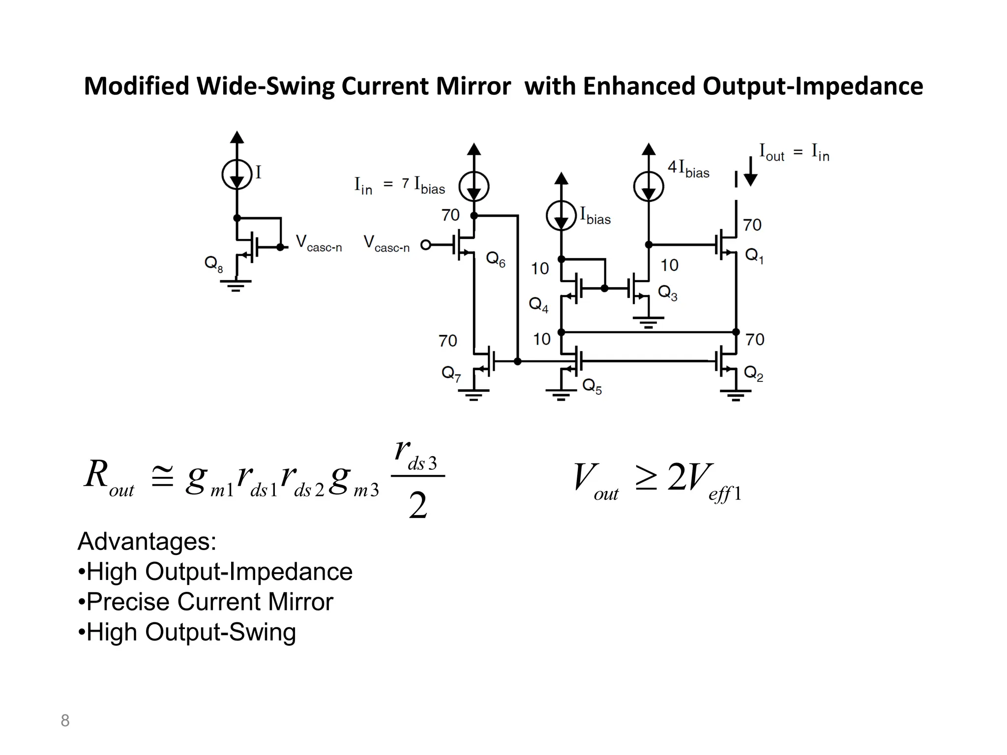
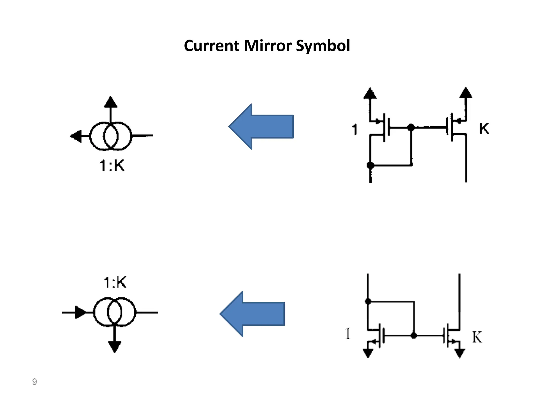
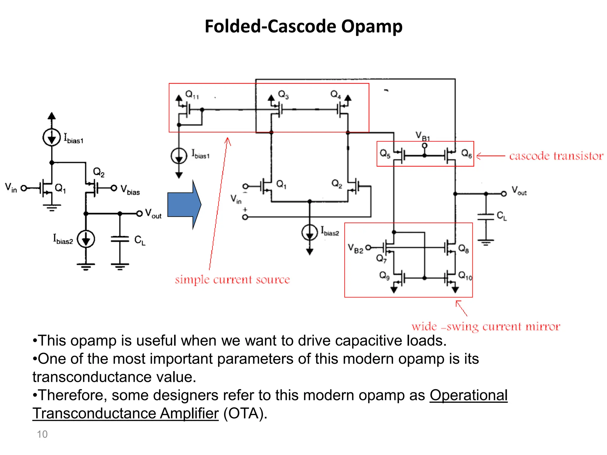
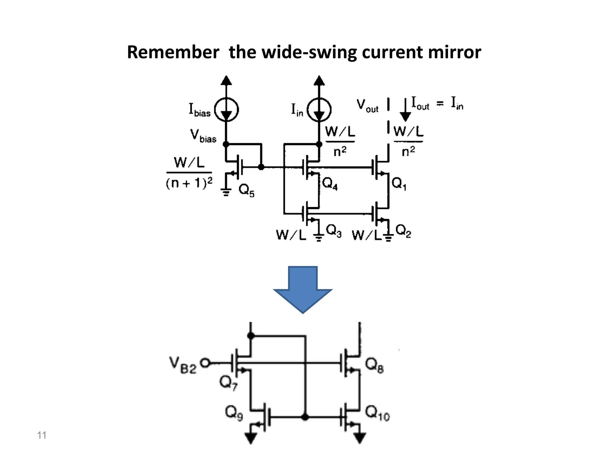
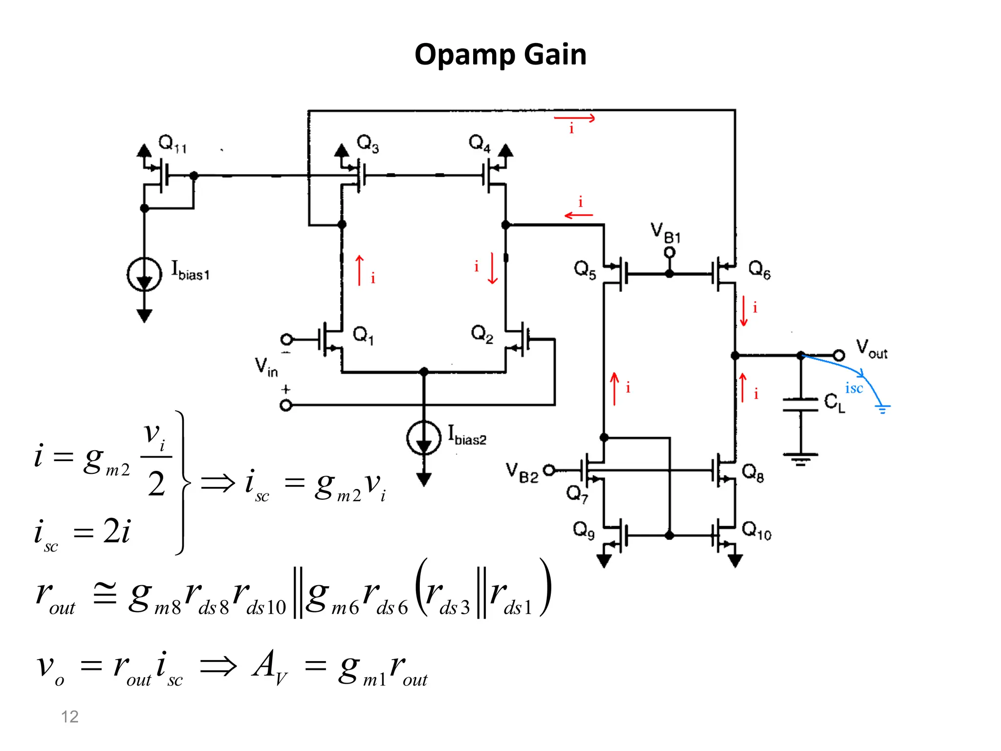
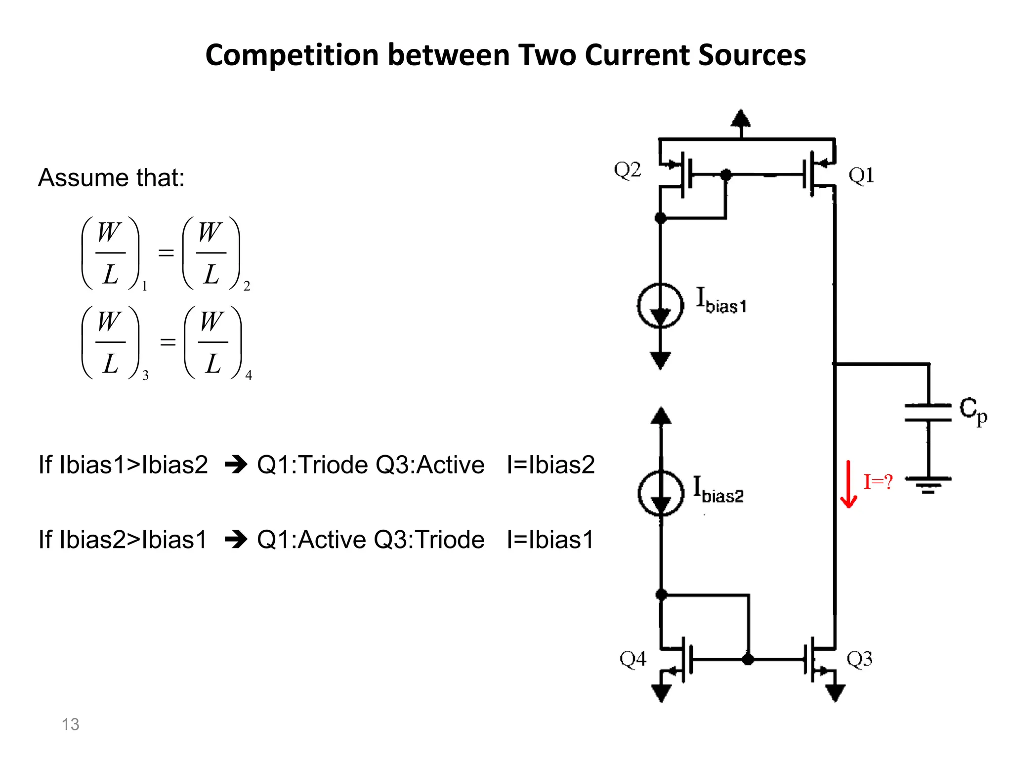
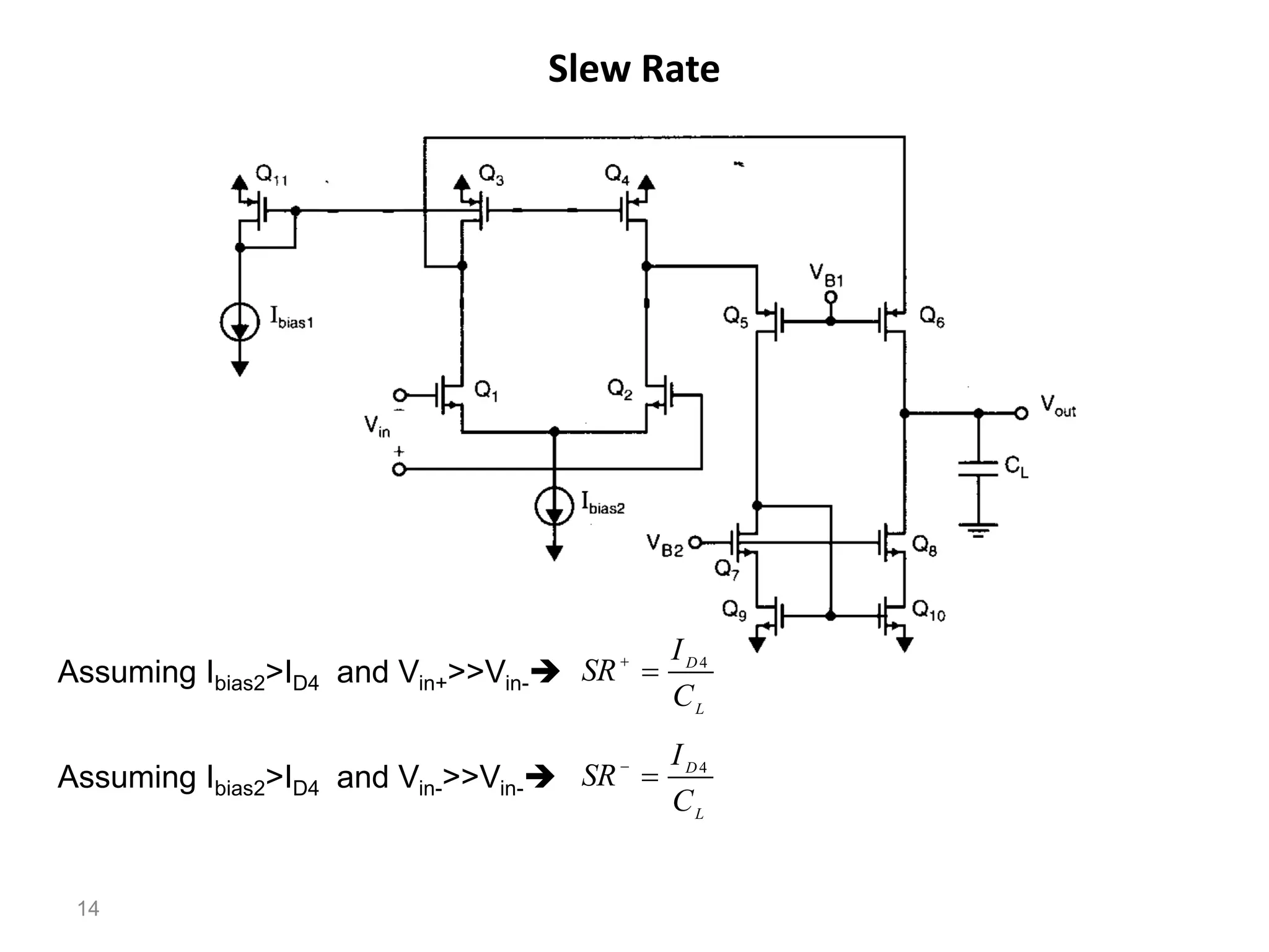
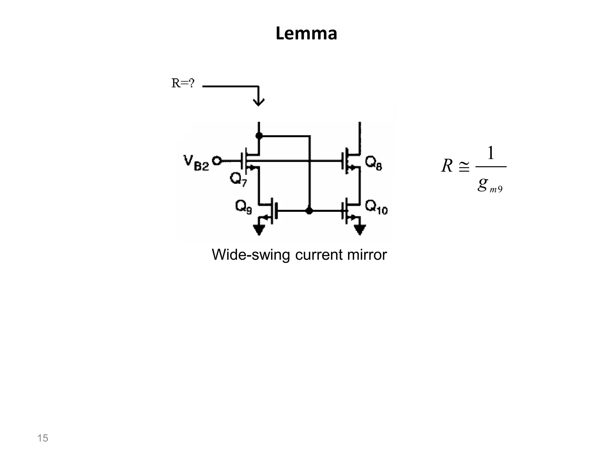
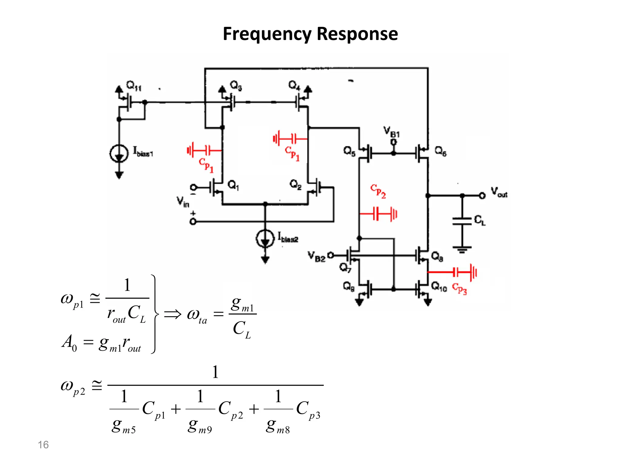
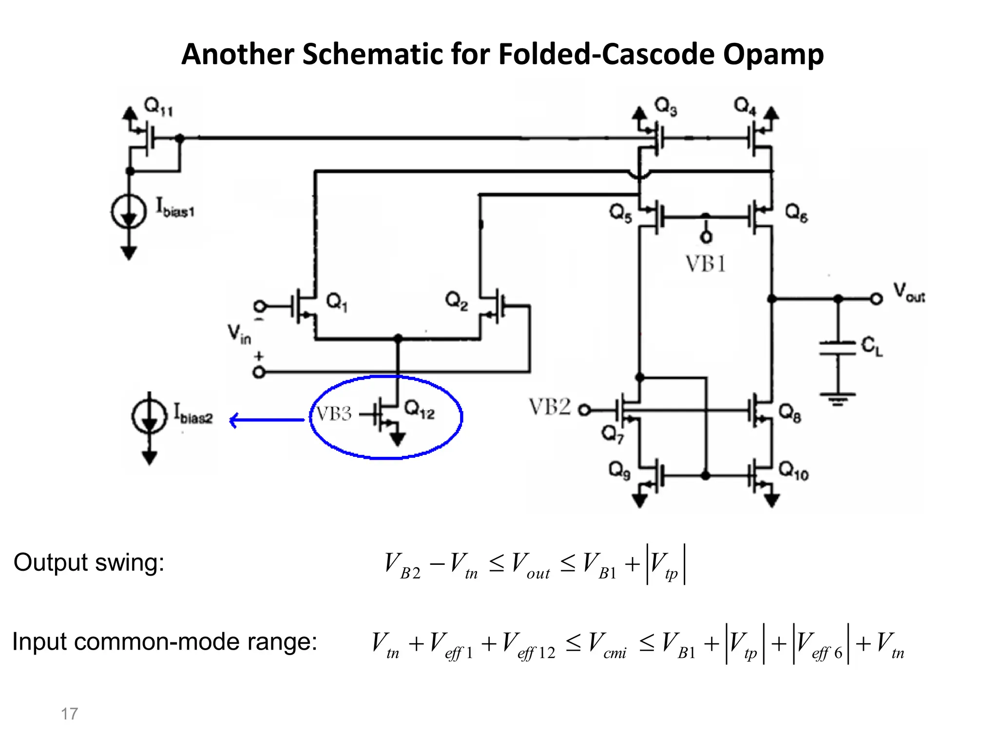
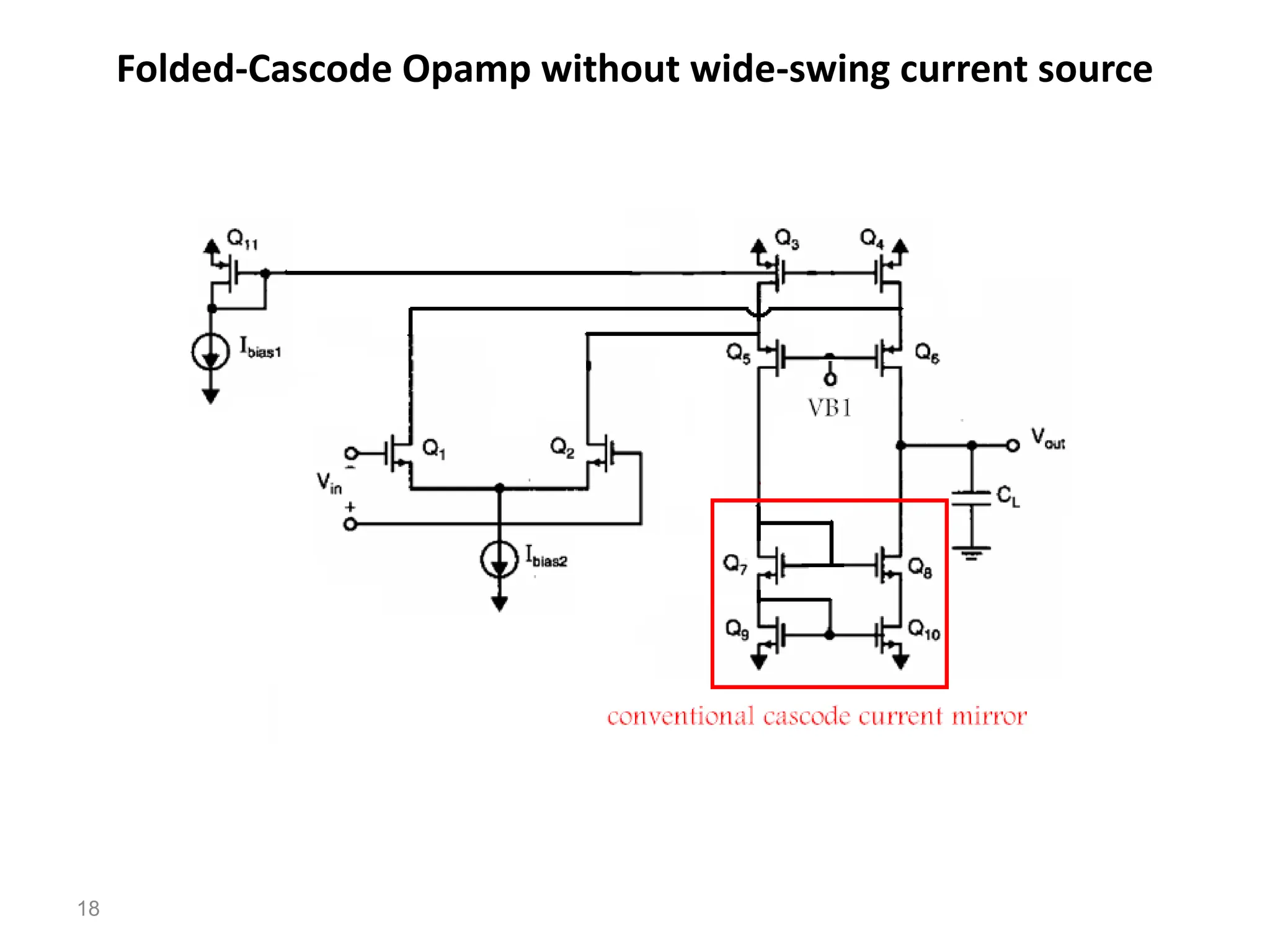
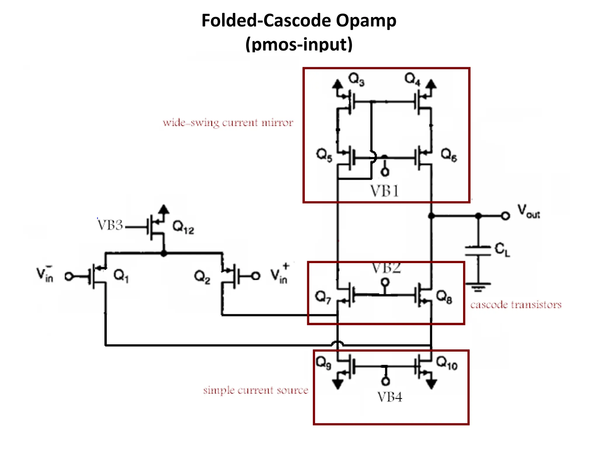
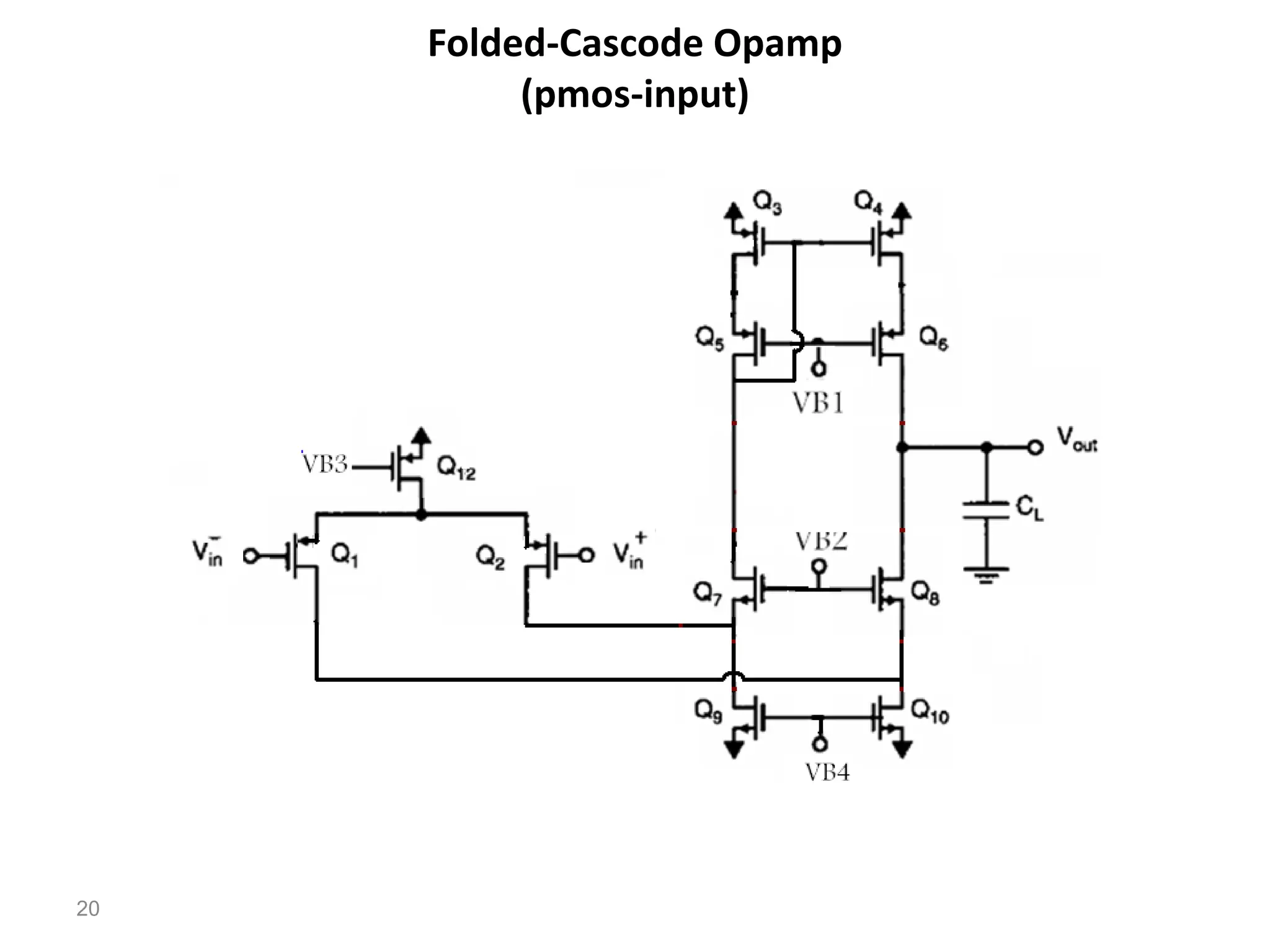
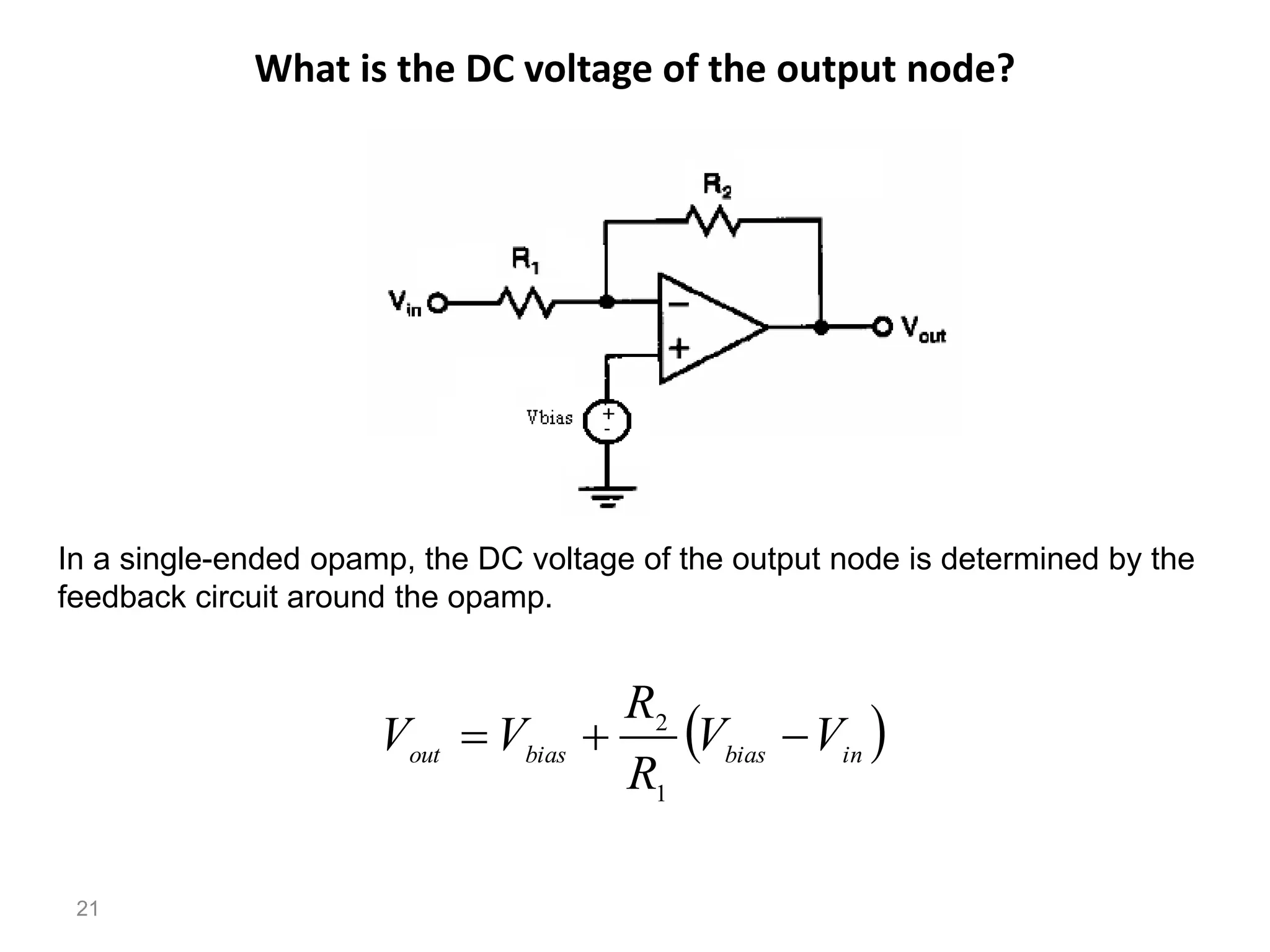
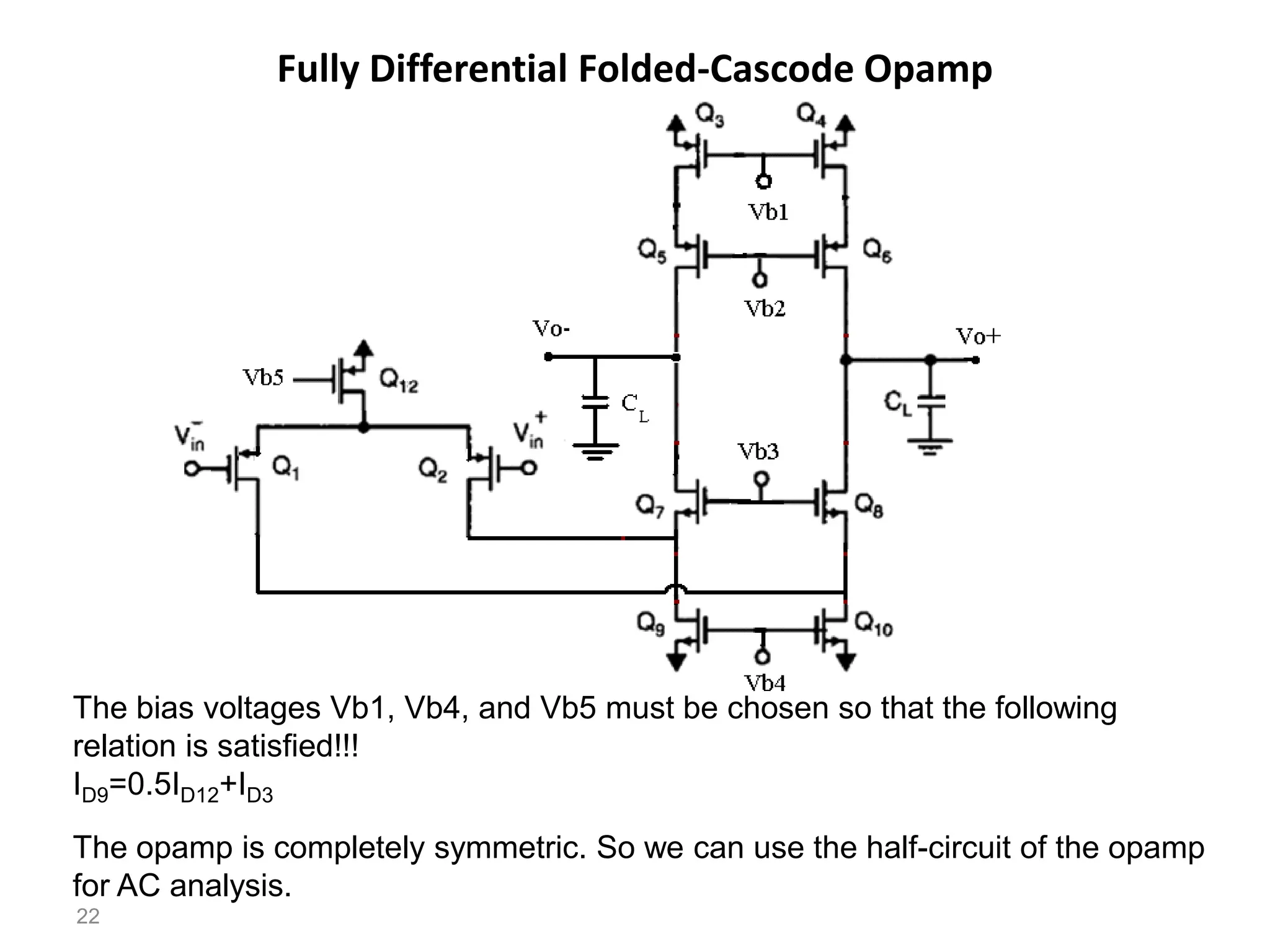
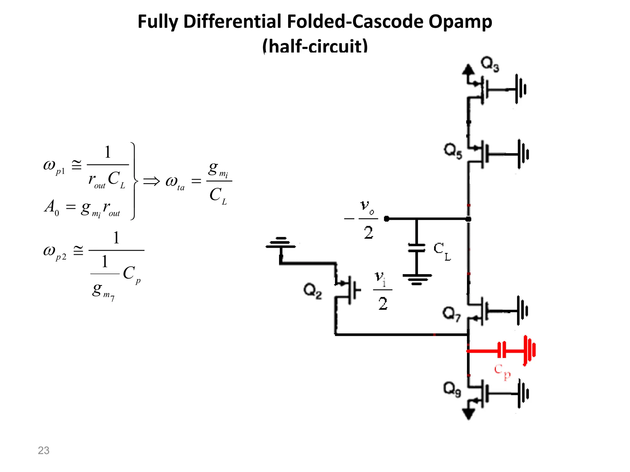
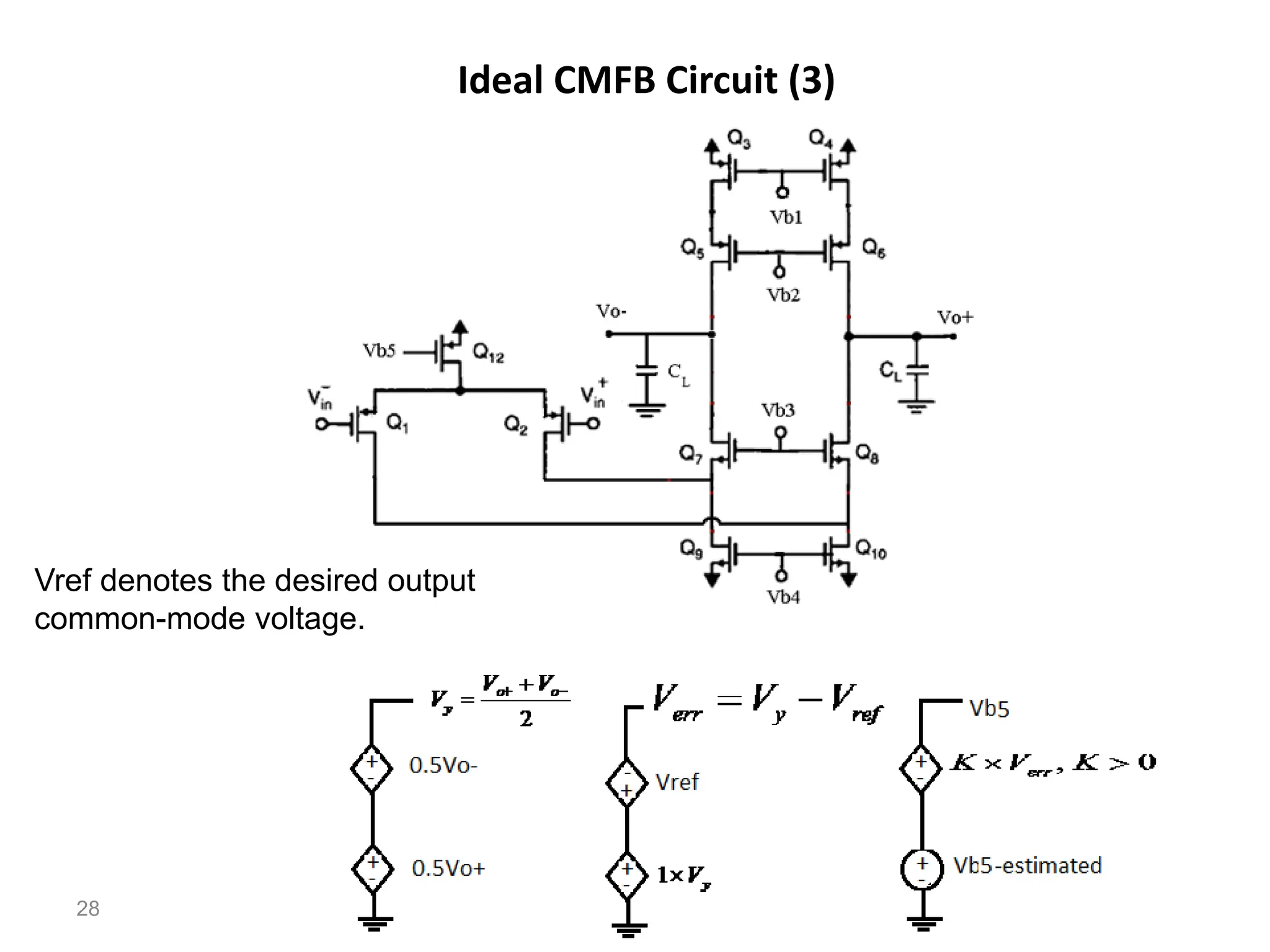
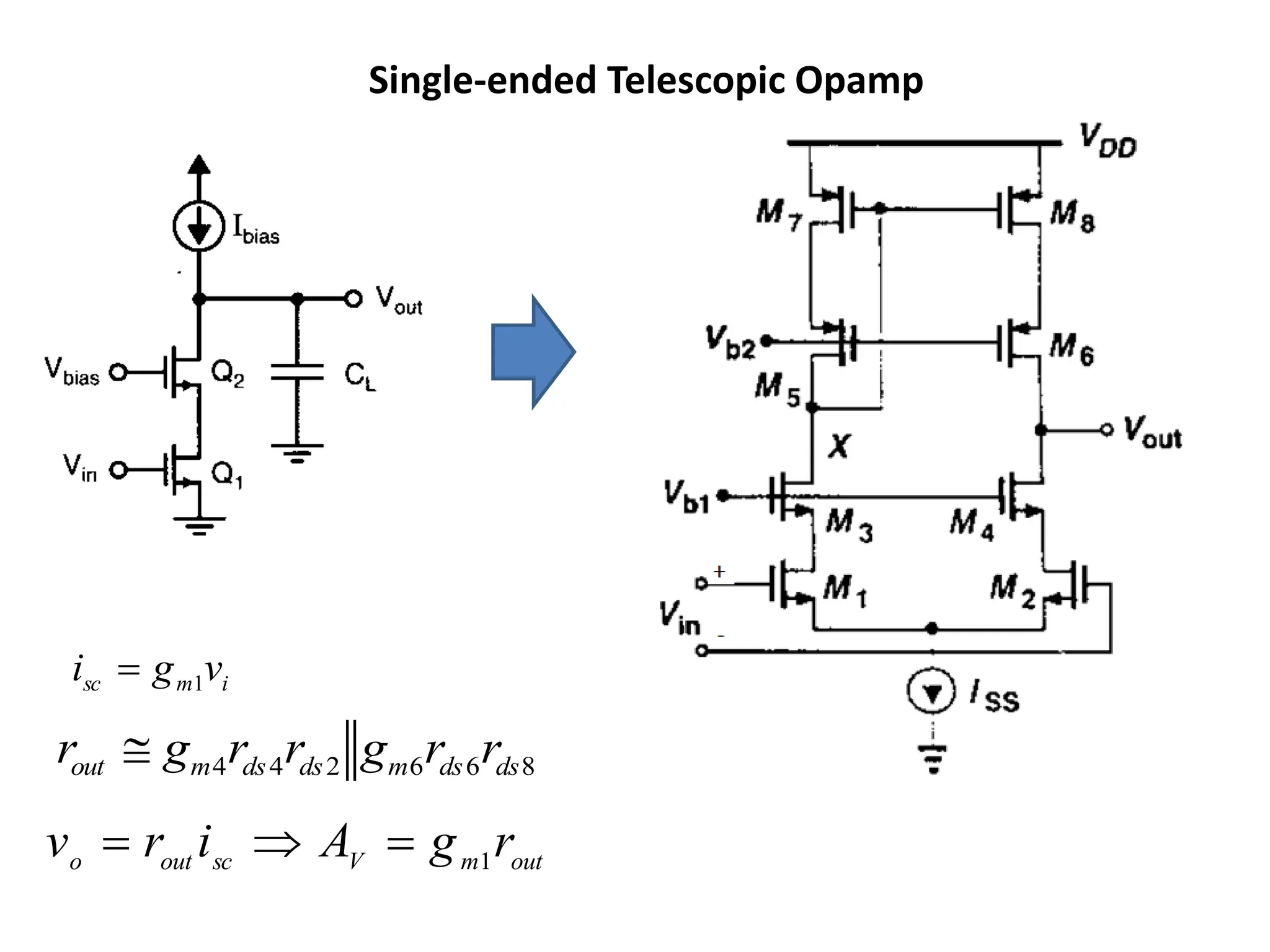
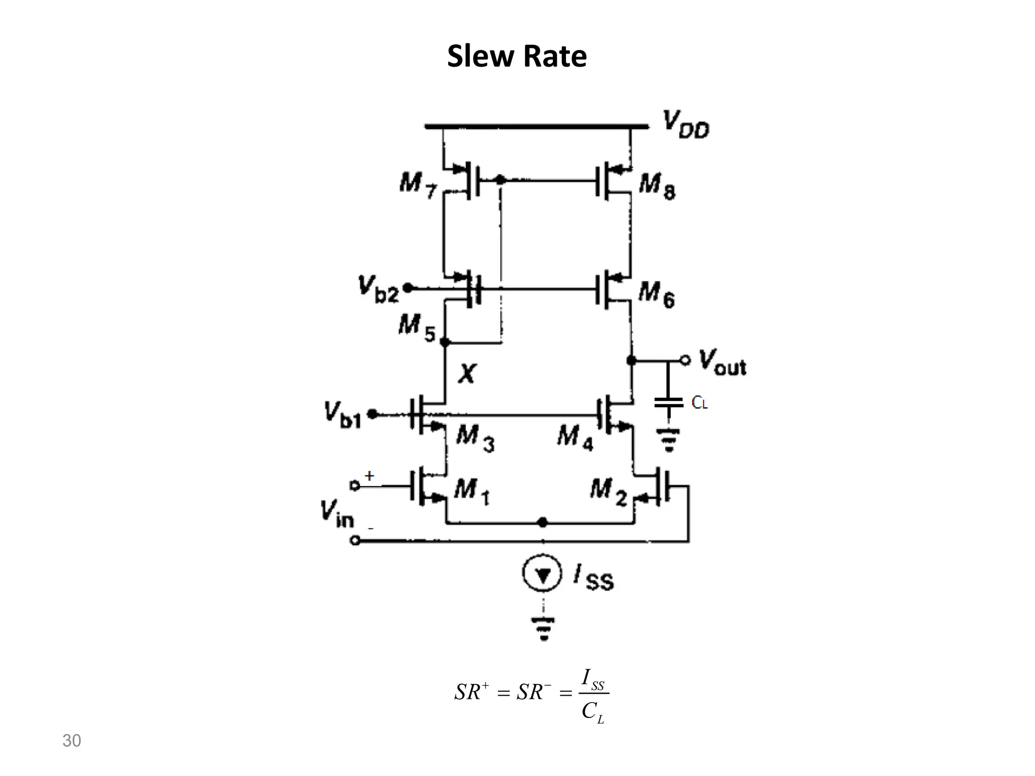
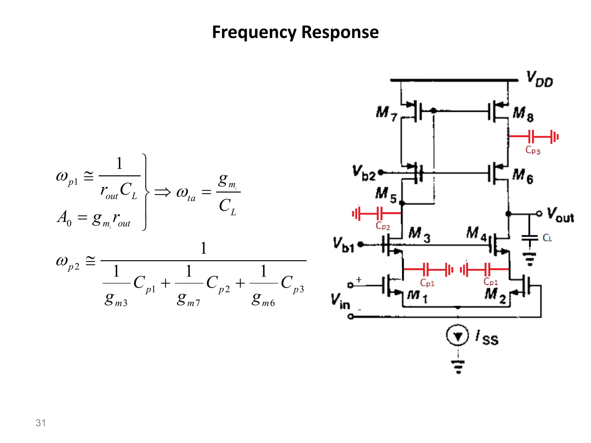
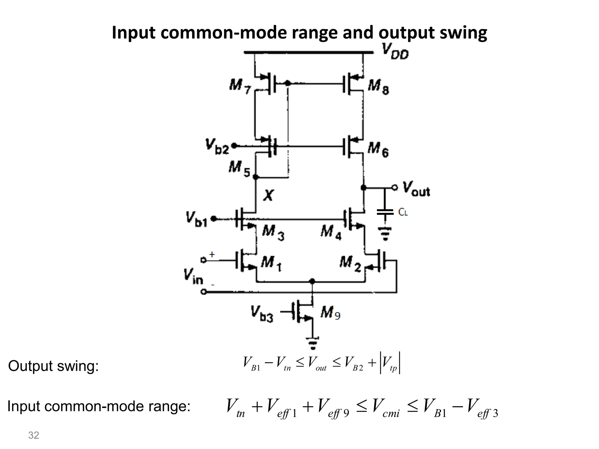
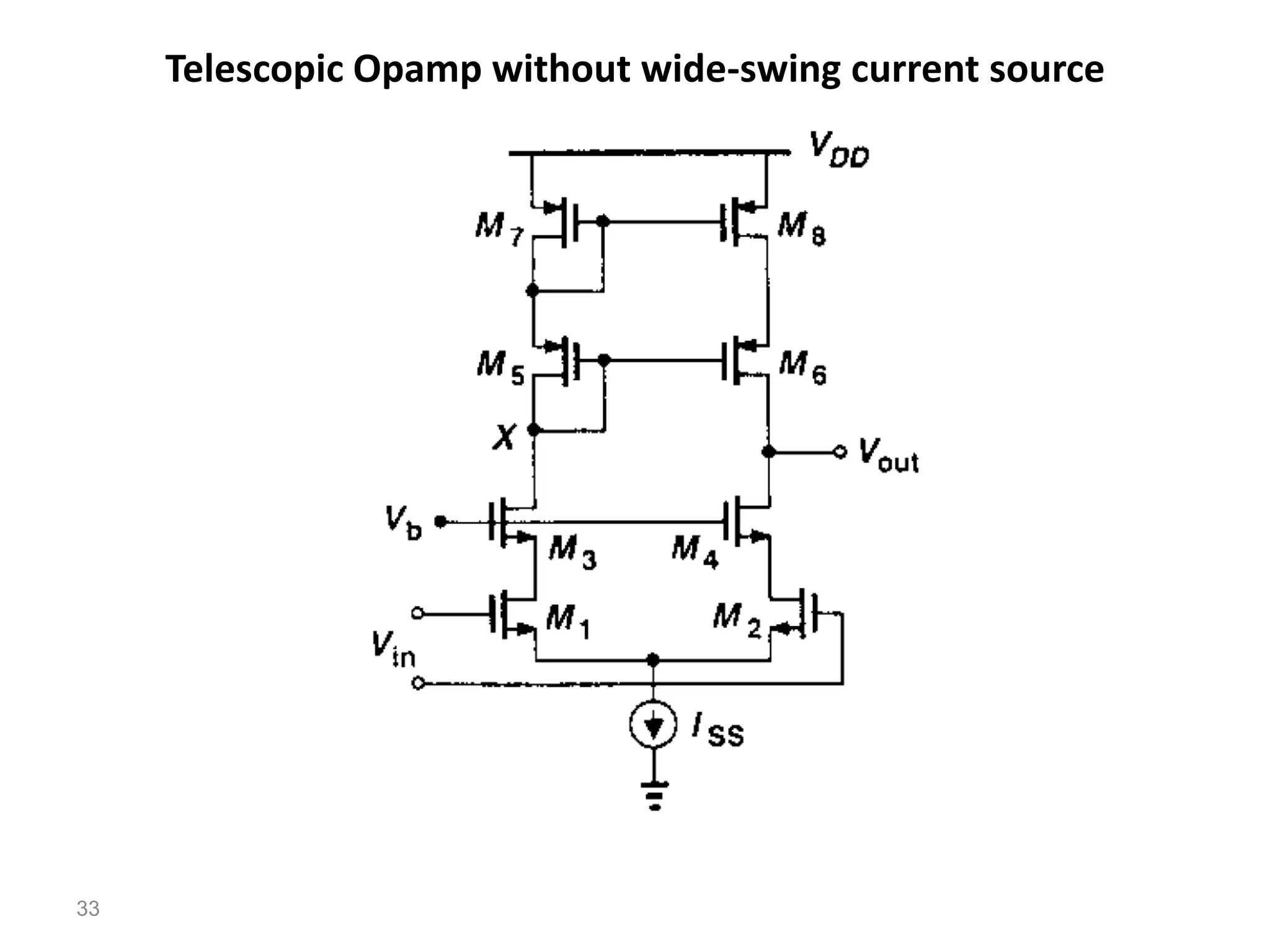
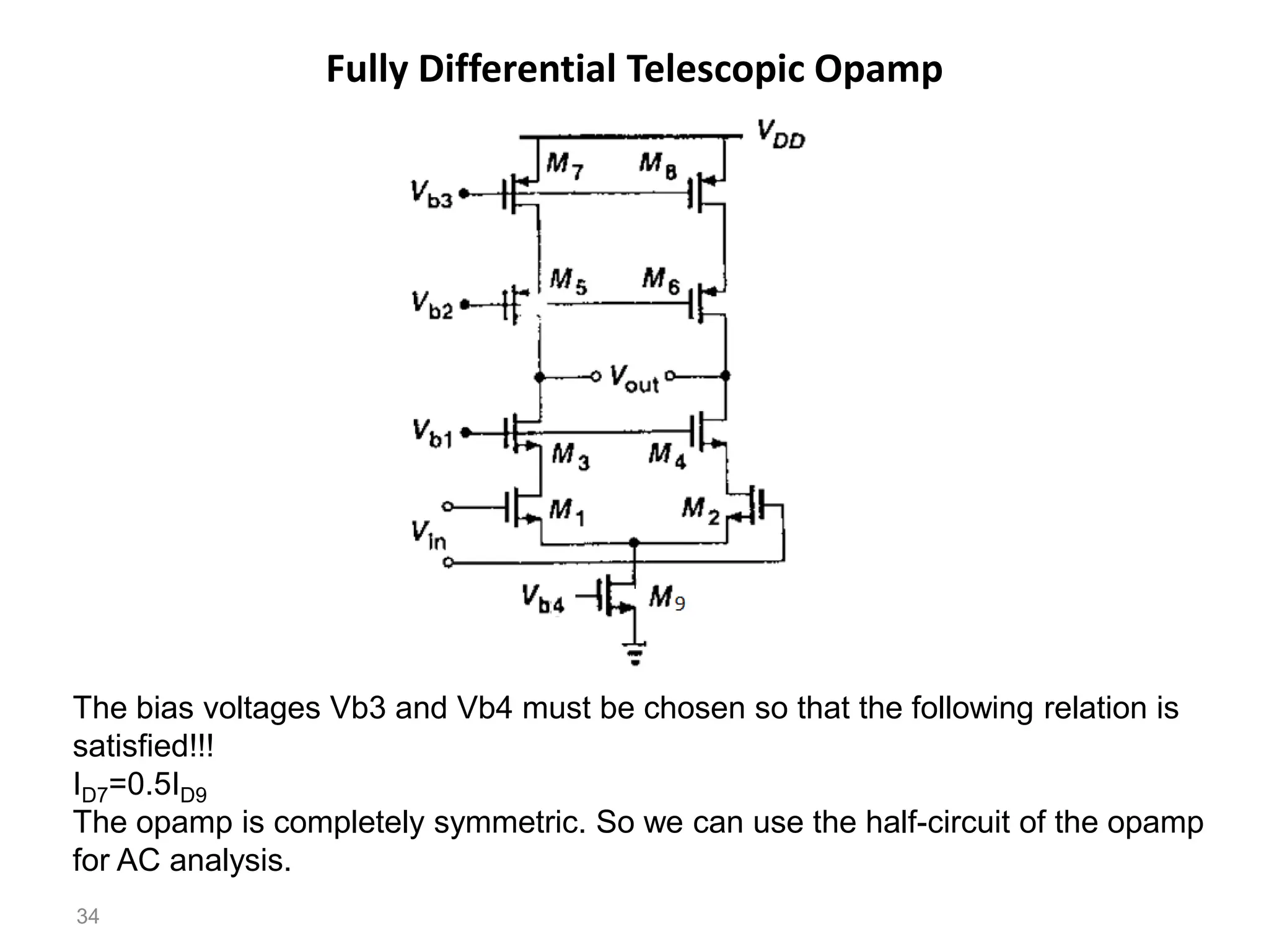
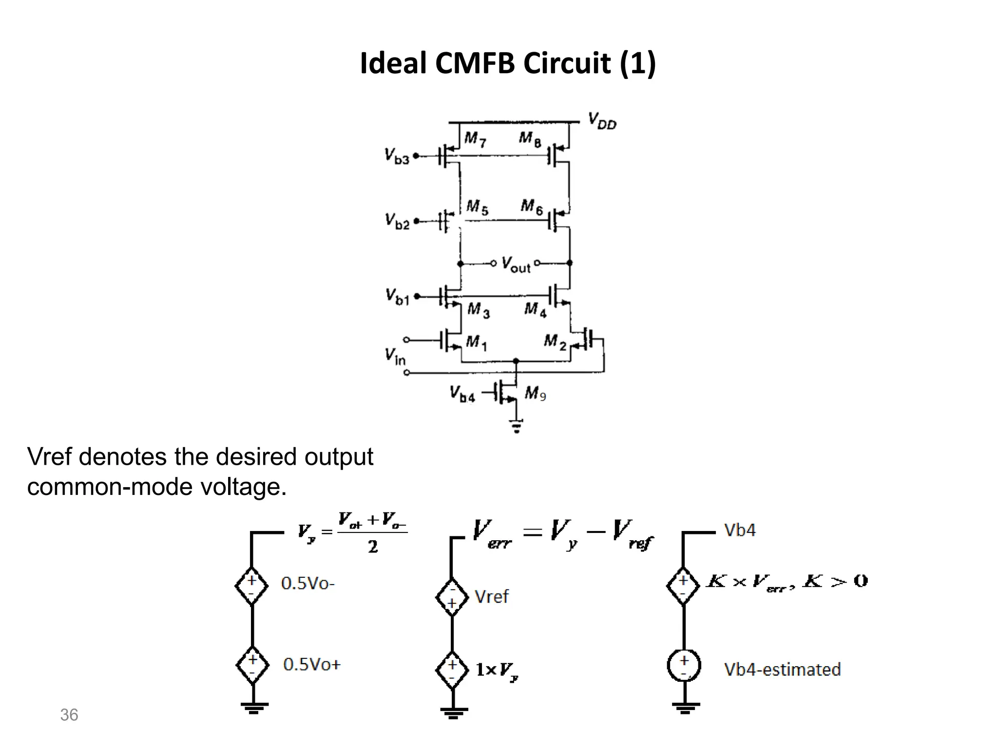
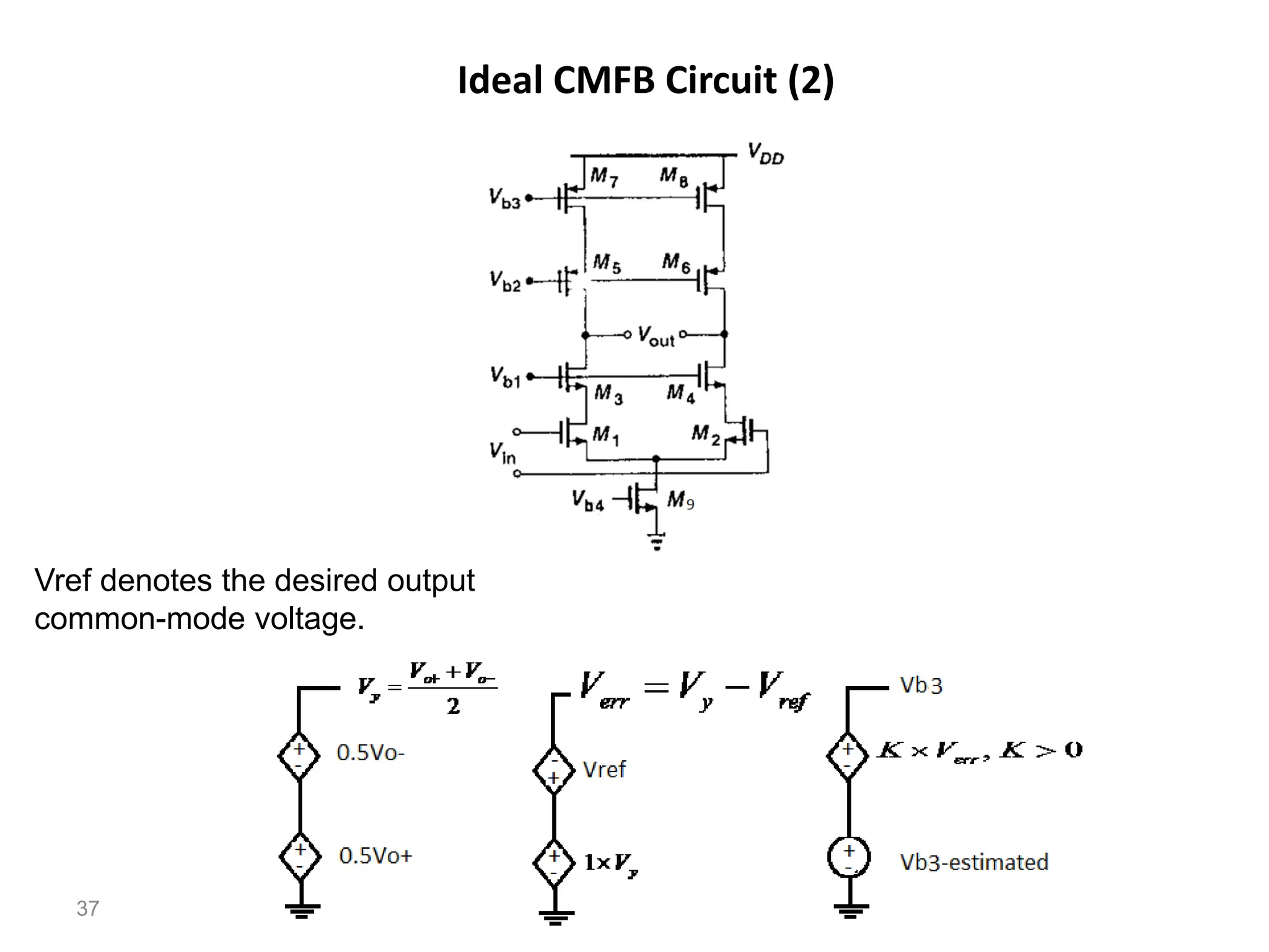
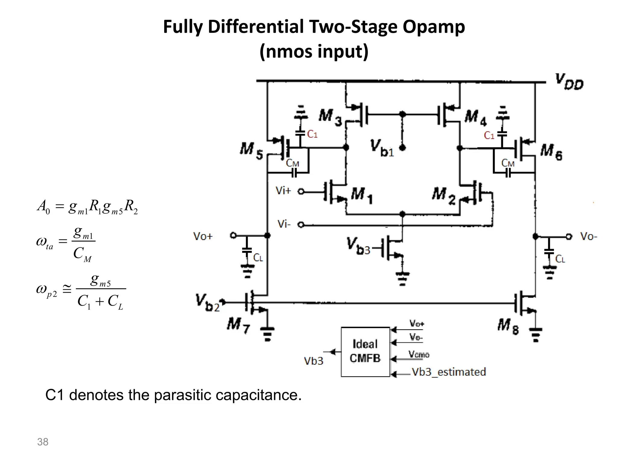
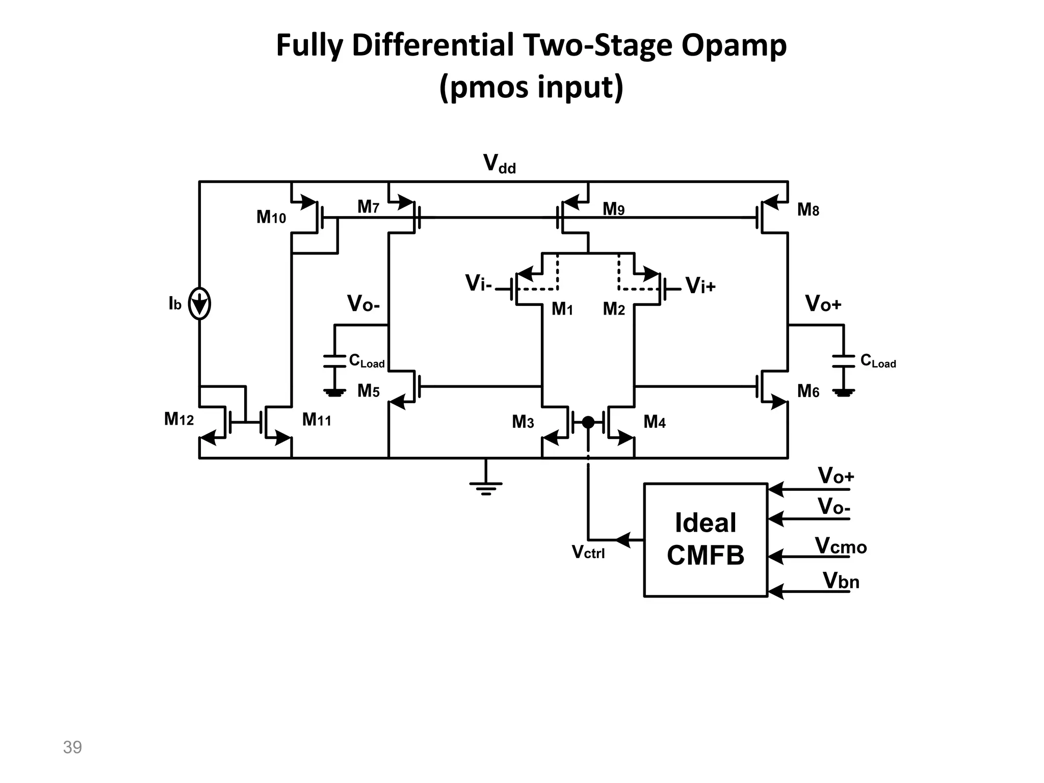
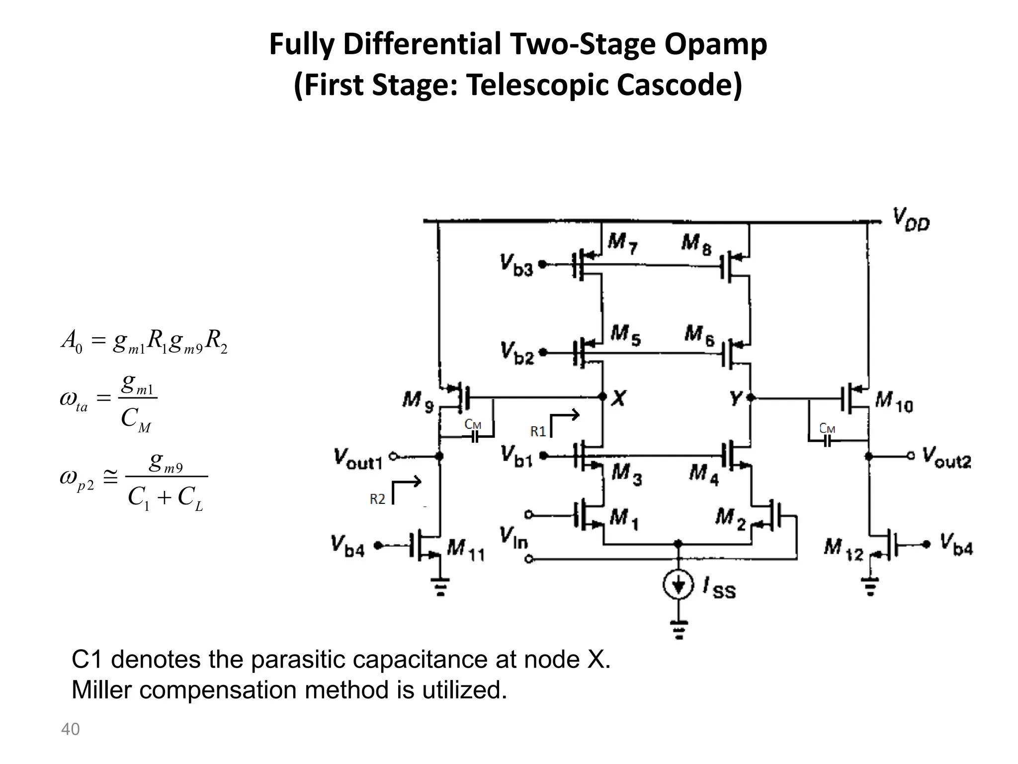
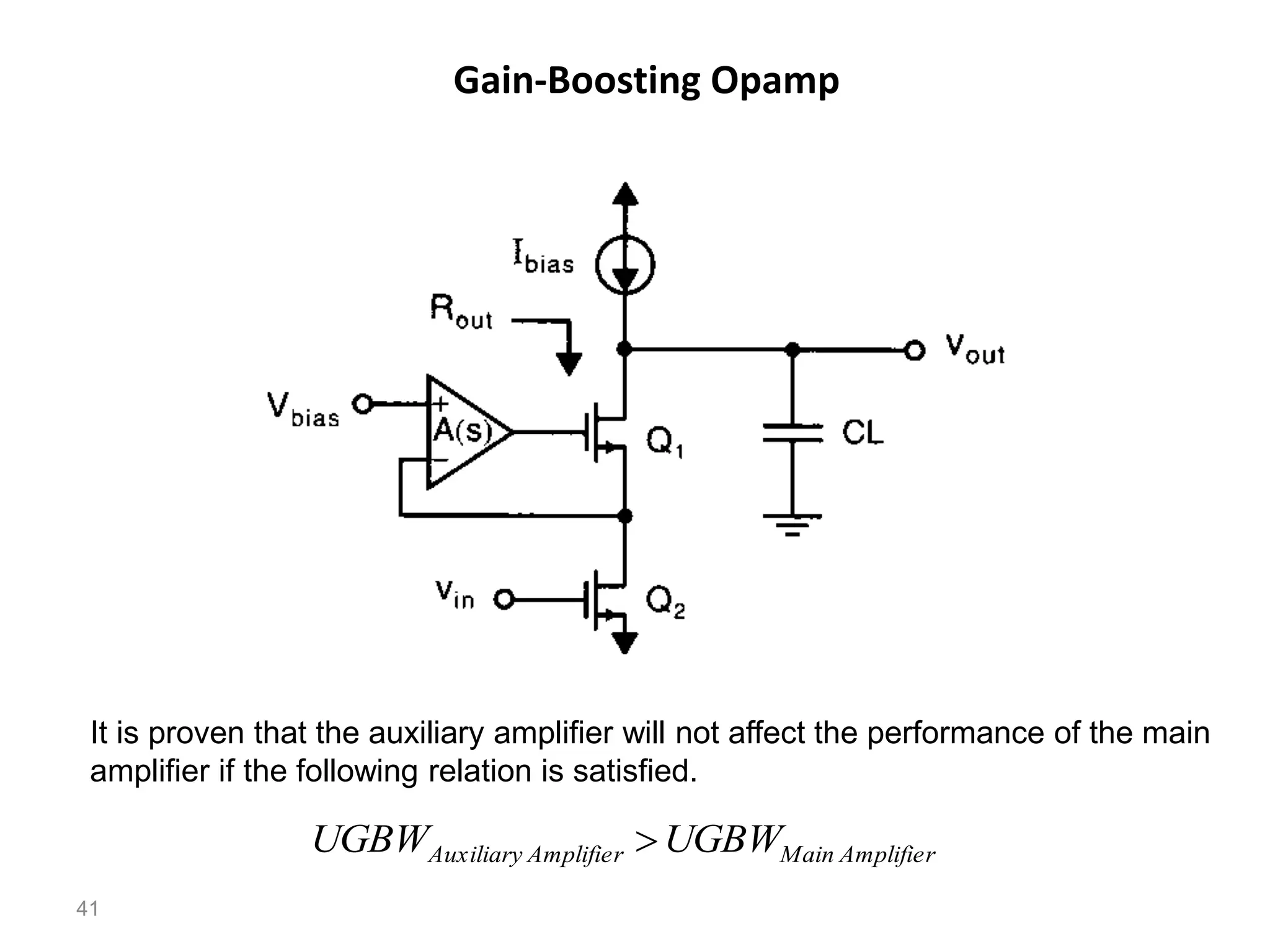
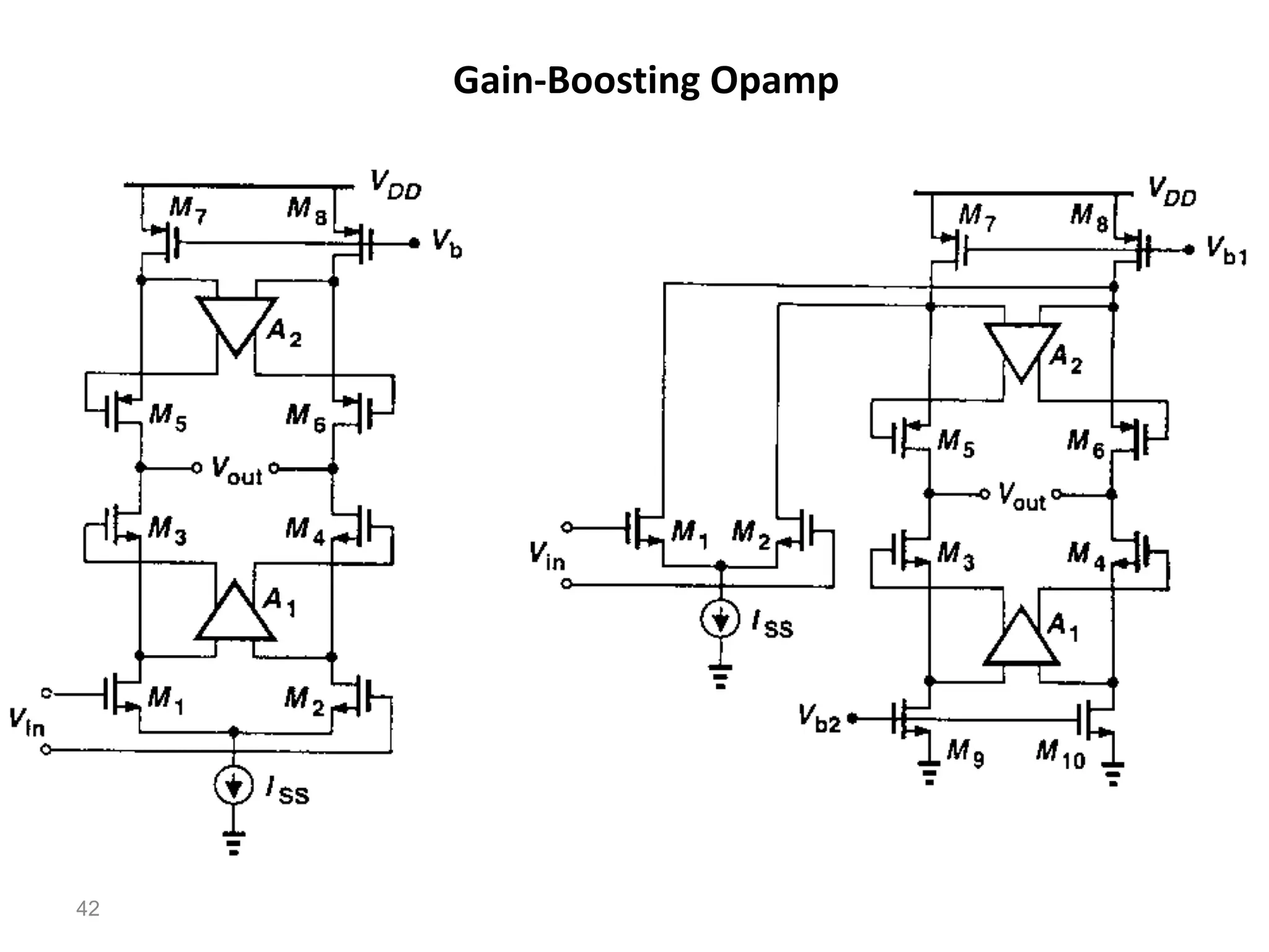
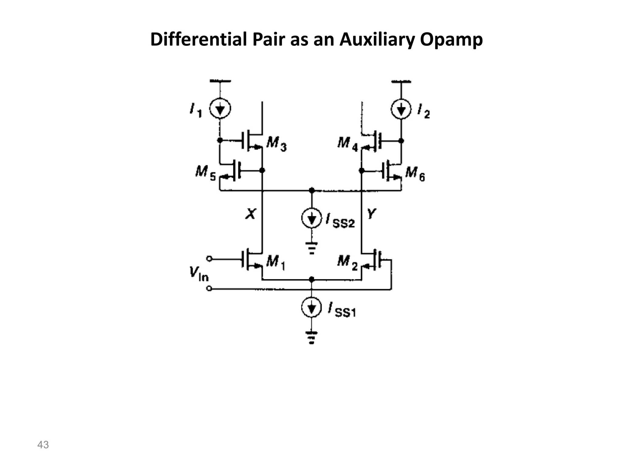
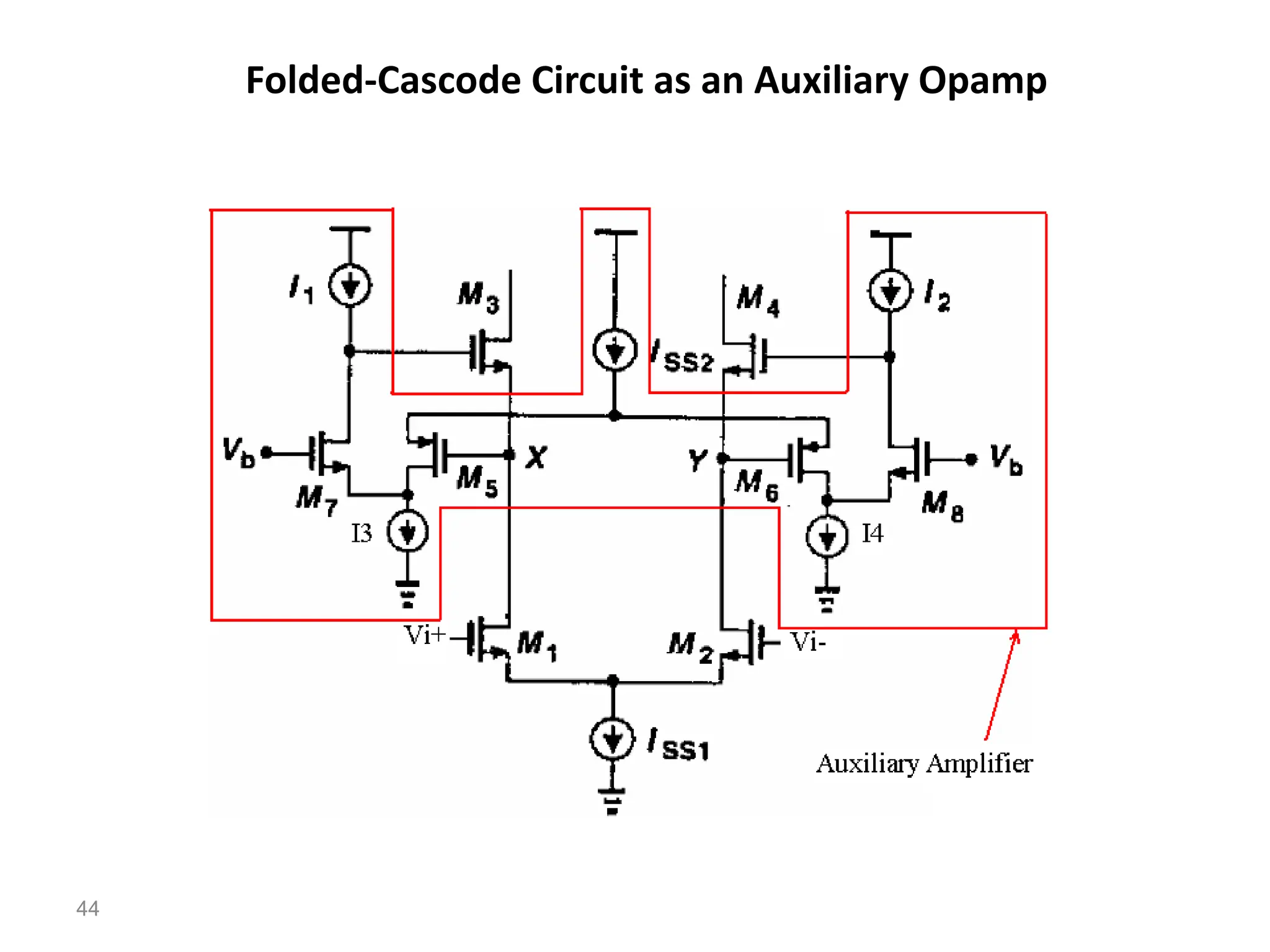
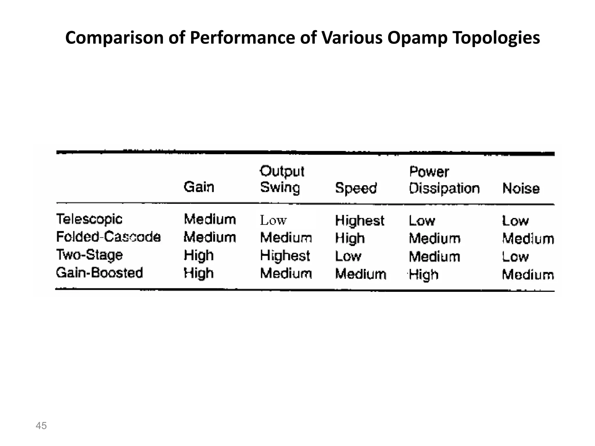
Advanced Current Mirrors and
Opamps
Hossein Shamsi
1
Wide-Swing Current Mirrors
2
It is proven that if both of the following conditions are satisfied, then all
transistors will be biased in the saturation region.
 








eff
tn
eff
out
nV
V
V
n
V 1
Typically n is chosen identical to 1. So the output swing will be:
eff
out
V
V 2

Enhanced Output-Impedance Current Mirrors
3
 
A
r
r
g
R ds
ds
m
out

 1
2
1
1
Implementation of Enhanced Output-Impedance Current
Mirror
4
1
3 eff
eff
tn
out
V
V
V
V 


2
3
3
2
1
1
ds
m
ds
ds
m
out
r
g
r
r
g
R 
Advantage:
•High Output-Impedance
Disadvantages:
•Low Output-Swing
•Imprecise Current Mirror
Implementation of Enhanced Output-Impedance Current
Mirror
5
1
3 eff
eff
tn
out
V
V
V
V 


2
3
3
2
1
1
ds
m
ds
ds
m
out
r
g
r
r
g
R 
Advantages:
•High Output-Impedance
•Precise Current Mirror
Disadvantage:
•Low Output-Swing
Implementation of Enhanced Output-Impedance Current
Mirror
6
1
2 eff
out
V
V 
2
3
3
2
1
1
ds
m
ds
ds
m
out
r
g
r
r
g
R  Advantages:
•High Output-Impedance
•High Output-Swing
Disadvantage:
•Imprecise Current Mirror
Wide-Swing Current Mirror with Enhanced Output-Impedance
7
1
2 eff
out
V
V 
2
3
3
2
1
1
ds
m
ds
ds
m
out
r
g
r
r
g
R 
Advantages:
•High Output-Impedance
•Precise Current Mirror
•High Output-Swing
Disadvantage:
•High Power Consumption
Modified Wide-Swing Current Mirror with Enhanced Output-Impedance
8
1
2 eff
out
V
V 
2
3
3
2
1
1
ds
m
ds
ds
m
out
r
g
r
r
g
R 
Advantages:
•High Output-Impedance
•Precise Current Mirror
•High Output-Swing
Current Mirror Symbol
9
Folded-Cascode Opamp
10
•This opamp is useful when we want to drive capacitive loads.
•One of the most important parameters of this modern opamp is its
transconductance value.
•Therefore, some designers refer to this modern opamp as Operational
Transconductance Amplifier (OTA).
Remember the wide-swing current mirror
11
Opamp Gain
12
i
m
sc
sc
i
m
v
g
i
i
i
v
g
i
2
2
2
2 








 
1
3
6
6
10
8
8 ds
ds
ds
m
ds
ds
m
out
r
r
r
g
r
r
g
r 
out
m
V
sc
out
o
r
g
A
i
r
v 1



Competition between Two Current Sources
13
If Ibias1>Ibias2  Q1:Triode Q3:Active I=Ibias2
If Ibias2>Ibias1  Q1:Active Q3:Triode I=Ibias1
Assume that:
4
3
2
1


























L
W
L
W
L
W
L
W
Slew Rate
14
Assuming Ibias2>ID4 and Vin+>>Vin-
L
D
C
I
SR 4


Assuming Ibias2>ID4 and Vin->>Vin-
L
D
C
I
SR 4


Lemma
15
9
1
m
g
R 
Wide-swing current mirror
Frequency Response
16
3
8
2
9
1
5
2
1
1
0
1
1
1
1
1
1
p
m
p
m
p
m
p
L
m
ta
out
m
L
out
p
C
g
C
g
C
g
C
g
r
g
A
C
r















Another Schematic for Folded-Cascode Opamp
17
tp
B
out
tn
B V
V
V
V
V 


 1
2
tn
eff
tp
B
cmi
eff
eff
tn V
V
V
V
V
V
V
V 





 6
1
12
1
Output swing:
Input common-mode range:
Folded-Cascode Opamp without wide-swing current source
18
Folded-Cascode Opamp
(pmos-input)
19
Folded-Cascode Opamp
(pmos-input)
20
What is the DC voltage of the output node?
21
In a single-ended opamp, the DC voltage of the output node is determined by the
feedback circuit around the opamp.
  

dc
Vout
 
in
bias
bias
out
V
V
R
R
V
V 


1
2
Fully Differential Folded-Cascode Opamp
22
The bias voltages Vb1, Vb4, and Vb5 must be chosen so that the following
relation is satisfied!!!
ID9=0.5ID12+ID3
The opamp is completely symmetric. So we can use the half-circuit of the opamp
for AC analysis.
Fully Differential Folded-Cascode Opamp
(half-circuit)
23
p
m
p
L
i
m
ta
out
i
m
L
out
p
C
g
C
g
r
g
A
C
r
7
2
0
1
1
1
1













What is the DC voltage of the output nodes?
24
In a single-ended opamp, the DC voltage of the output node is determined by the
feedback circuit around the opamp.
  

dc
Vout
  CM
x
o
o
o
x
CM
o
CM
o
CM
x
CM
V
V
V
V
V
V
V
V
V
RI
V
V
R
V
V
I



















 2
2
2
The DC voltage of the output nodes can not be determined!!!
CM
i
i V
V
V 
 

Common-Mode Feedback Circuit
(CMFB Circuit)
25
In a fully differential opamp, the CMFB circuit is employed inside the opamp to
adjust the common-mode voltage of the output nodes identical to a
predetermined voltage, Vref.
CM
x
o
V
V
V
KCL
and
KVL 

 2
ref
o
o
V
V
V
Circuit
CMFB 

 

2
2
CM
ref
x
ref
o
o
V
V
V
V
V
V



 

Ideal CMFB Circuit (1)
26
Vref denotes the desired output
common-mode voltage.
Ideal CMFB Circuit (2)
27
Vref denotes the desired output
common-mode voltage.
Ideal CMFB Circuit (3)
28
Vref denotes the desired output
common-mode voltage.
Single-ended Telescopic Opamp
i
m
sc v
g
i 1

8
6
6
2
4
4 ds
ds
m
ds
ds
m
out r
r
g
r
r
g
r 
out
m
V
sc
out
o
r
g
A
i
r
v 1



Slew Rate
30
L
SS
C
I
SR
SR 
 

Frequency Response
31
3
6
2
7
1
3
2
0
1
1
1
1
1
1
p
m
p
m
p
m
p
L
m
ta
out
m
L
out
p
C
g
C
g
C
g
C
g
r
g
A
C
r i
i















Input common-mode range and output swing
32
tp
B
out
tn
B V
V
V
V
V 


 2
1
3
1
9
1 eff
B
cmi
eff
eff
tn V
V
V
V
V
V 




Output swing:
Input common-mode range:
Telescopic Opamp without wide-swing current source
33
Fully Differential Telescopic Opamp
34
The bias voltages Vb3 and Vb4 must be chosen so that the following relation is
satisfied!!!
ID7=0.5ID9
The opamp is completely symmetric. So we can use the half-circuit of the opamp
for AC analysis.
Fully Differential Telescopic Opamp
(half-circuit)
35
p
m
p
L
m
ta
out
m
L
out
p
C
g
C
g
r
g
A
C
r
3
2
1
1
0
1
1
1
1













Ideal CMFB Circuit (1)
36
Vref denotes the desired output
common-mode voltage.
Ideal CMFB Circuit (2)
37
Vref denotes the desired output
common-mode voltage.
Fully Differential Two-Stage Opamp
(nmos input)
38
L
m
p
M
m
ta
m
m
C
C
g
C
g
R
g
R
g
A




1
5
2
1
2
5
1
1
0


C1 denotes the parasitic capacitance.
Fully Differential Two-Stage Opamp
(pmos input)
39
Vo+
Vdd
Ib M1 M2
M3 M4
M5 M6
M7 M8
M9
M10
M11
M12
Vo-
Vi+
Vi-
Vctrl
Ideal
CMFB
Vo+
Vo-
Vbn
Vcmo
CLoad
CLoad
40
Fully Differential Two-Stage Opamp
(First Stage: Telescopic Cascode)
C1 denotes the parasitic capacitance at node X.
Miller compensation method is utilized.
L
m
p
M
m
ta
m
m
C
C
g
C
g
R
g
R
g
A




1
9
2
1
2
9
1
1
0


41
Gain-Boosting Opamp
It is proven that the auxiliary amplifier will not affect the performance of the main
amplifier if the following relation is satisfied.
Amplifier
Main
Amplifier
Auxiliary UGBW
UGBW 
42
Gain-Boosting Opamp
43
Differential Pair as an Auxiliary Opamp
44
Folded-Cascode Circuit as an Auxiliary Opamp
45
Comparison of Performance of Various Opamp Topologies

Slide4-1.pdf