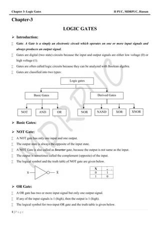
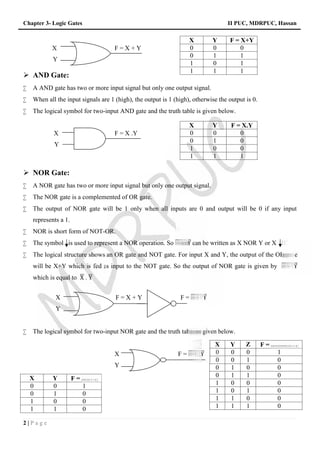
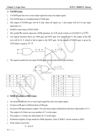
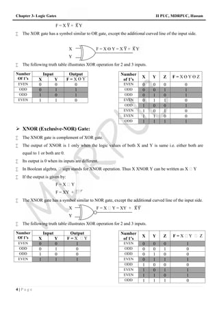
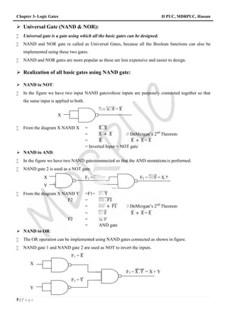
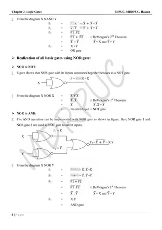
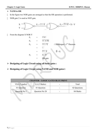
Chapter 3- Logic Gates II PUC, MDRPUC, Hassan
1 | P a g e
Chapter-3
LOGIC GATES
 Introduction:
 Gate: A Gate is a simply an electronic circuit which operates on one or more input signals and
always produces an output signal.
 Gates are digital (two state) circuits because the input and output signals are either low voltage (0) or
high voltage (1).
 Gates are often called logic circuits because they can be analyzed with Boolean algebra.
 Gates are classified into two types:
 Basic Gates:
 NOT Gate:
 A NOT gate has only one input and one output.
 The output state is always the opposite of the input state.
 A NOT Gate is also called as Inverter gate, because the output is not same as the input.
 The output is sometimes called the complement (opposite) of the input.
 The logical symbol and the truth table of NOT gate are given below.
X X
 OR Gate:
 A OR gate has two or more input signal but only one output signal.
 If any of the input signals is 1 (high), then the output is 1 (high).
 The logical symbol for two-input OR gate and the truth table is given below.
X
0 1
1 0
Logic gates
Basic Gates Derived Gates
AND OR NOR NAND XOR
NOT XNOR
Chapter 3- Logic Gates II PUC, MDRPUC, Hassan
2 | P a g e
X F = X + Y
Y
 AND Gate:
 A AND gate has two or more input signal but only one output signal.
 When all the input signals are 1 (high), the output is 1 (high), otherwise the output is 0.
 The logical symbol for two-input AND gate and the truth table is given below.
X F = X .Y
Y
 NOR Gate:
 A NOR gate has two or more input signal but only one output signal.
 The NOR gate is a complemented of OR gate.
 The output of NOR gate will be 1 only when all inputs are 0 and output will be 0 if any input
represents a 1.
 NOR is short form of NOT-OR.
 The symbol is used to represent a NOR operation. So X + Y can be written as X NOR Y or X Y.
 The logical structure shows an OR gate and NOT gate. For input X and Y, the output of the OR gate
will be X+Y which is fed as input to the NOT gate. So the output of NOR gate is given by X + Y
which is equal to X . Y
X F = X + Y F = X + Y
Y
 The logical symbol for two-input NOR gate and the truth table is given below.
X F = X + Y
Y
X Y F = X+Y
0 0 0
0 1 1
1 0 1
1 1 1
X Y F = X.Y
0 0 0
0 1 0
1 0 0
1 1 1
X Y Z F = + +
0 0 0 1
0 0 1 0
0 1 0 0
0 1 1 0
1 0 0 0
1 0 1 0
1 1 0 0
1 1 1 0
X Y F = +
0 0 1
0 1 0
1 0 0
1 1 0
Chapter 3- Logic Gates II PUC, MDRPUC, Hassan
3 | P a g e
 NAND Gate:
 A NAND gate has two or more input signal but only one output signal.
 The NAND gate is a complemented of AND gate.
 The output of NAND gate will be 0 only when all inputs are 1 and output will be 0 if any input
represents a 0.
 NAND is short form of NOT-AND.
 The symbol is used to represent a NOR operation. So X . Y can be written as X NAND Y or X Y.
 The logical structure shows an AND gate and NOT gate. For input X and Y, the output of the OR
gate will be X .Y which is fed as input to the NOT gate. So the output of NAND gate is given by
X . Y which is equal to X + Y
X F = X . Y F = X . Y
Y
 The logical symbol for two-input NAND gate and the truth table is given below.
X F = X . Y
Y
 XOR (Exclusive-OR) Gate:
 An exclusive-OR has two or more input signal but only one output signal.
 Exclusive-OR gate is different form of OR gate.
 Exclusive-OR gate produces output 1 for only those input combinations that have odd number of 1’s.
 The output is 0 if there are even number of 1’s in the input.
 The output is 1 if there are odd number of 1’s in the input.
 In Boolean algebra, ϴ sign stands for XOR operation. Thus X XOR Y can be written as XϴY
 If the output is given by:
F = X ϴ Y
X Y F = .
0 0 1
0 1 1
1 0 1
1 1 0
X Y Z F = . .
0 0 0 1
0 0 1 1
0 1 0 1
0 1 1 1
1 0 0 1
1 0 1 1
1 1 0 1
1 1 1 0
Chapter 3- Logic Gates II PUC, MDRPUC, Hassan
4 | P a g e
F = X Y + X Y
 The XOR gate has a symbol similar to OR gate, except the additional curved line of the input side.
X F = X ϴ Y = X Y + X Y
Y
 The following truth table illustrates XOR operation for 2 and 3 inputs.
 XNOR (Exclusive-NOR) Gate:
 The XNOR gate is complement of XOR gate.
 The output of XNOR is 1 only when the logic values of both X and Y is same i.e. either both are
equal to 1 or both are 0.
 Its output is 0 when its inputs are different.
 In Boolean algebra, ʘ sign stands for XNOR operation. Thus X XNOR Y can be written as X ʘ Y
 If the output is given by:
F = X ʘ Y
F = XY + XY
 The XNOR gate has a symbol similar to NOR gate, except the additional curved line of the input side.
X F = X ʘ Y = XY + X Y
Y
 The following truth table illustrates XOR operation for 2 and 3 inputs.
Number
Of 1’s
Input Output
X Y F = X ϴ Y
EVEN 0 0 0
ODD 0 1 1
ODD 1 0 1
EVEN 1 1 0
Number
of 1’s
X Y Z F = X ϴ Y ϴ Z
EVEN 0 0 0 0
ODD 0 0 1 1
ODD 0 1 0 1
EVEN 0 1 1 0
ODD 1 0 0 1
EVEN 1 0 1 0
EVEN 1 1 0 0
ODD 1 1 1 1
Number
Of 1’s
Input Output
X Y F = X ʘ Y
EVEN 0 0 1
ODD 0 1 0
ODD 1 0 0
EVEN 1 1 1
Number
of 1’s
X Y Z F = X ʘ Y ʘ Z
EVEN 0 0 0 1
ODD 0 0 1 0
ODD 0 1 0 0
EVEN 0 1 1 1
ODD 1 0 0 0
EVEN 1 0 1 1
EVEN 1 1 0 1
ODD 1 1 1 0
Chapter 3- Logic Gates II PUC, MDRPUC, Hassan
5 | P a g e
 Universal Gate (NAND & NOR):
 Universal gate is a gate using which all the basic gates can be designed.
 NAND and NOR gate re called as Universal Gates, because all the Boolean functions can also be
implemented using these two gates.
 NAND and NOR gates are more popular as these are less expensive and easier to design.
 Realization of all basic gates using NAND gate:
 NAND to NOT:
 In the figure we have two input NAND gate whose inputs are purposely connected together so that
the same input is applied to both.
F = X . X = X
X
 From the diagram X NAND X = X . X
= X + X // DeMorgan’s 2nd
Theorem
= X X + X = X
= Inverted Input = NOT gate
 NAND to AND:
 In the figure we have two NAND gates connected so that the AND operations is performed.
 NAND gate 2 is used as a NOT gate.
X F1 = X . Y F2 = X. Y = X.Y
Y
 From the diagram X NAND Y =F1= X . Y
F2 = F1 . F1
= F1 + F1 // DeMorgan’s 2nd
Theorem
= X. Y X + X = X
F2 = X.Y
= AND gate
 NAND to OR:
 The OR operation can be implemented using NAND gates connected as shown in figure.
 NAND gate 1 and NAND gate 2 are used as NOT to invert the inputs.
F1 = X
X
F3 = X . Y = X + Y
F2 = Y
Y
Chapter 3- Logic Gates II PUC, MDRPUC, Hassan
6 | P a g e
 From the diagram X NAND Y
F1 = X . X = X + X = X
F2 = Y . Y = Y + Y = Y
F3 = F1 . F2
= F1 + F2 // DeMorgan’s 2nd
Theorem
= X + Y X = X and Y = Y
F3 = X +Y
= OR gate
 Realization of all basic gates using NOR gate:
 NOR to NOT:
 Figure shows that NOR gate with its inputs connected together behaves as a NOT gate.
F = X + X = X
X
 From the diagram X NOR X = X + X
= X . X // DeMorgan’s 1st
Theorem
= X X . X = X
= Inverted Input = NOT gate
 NOR to AND:
 The AND operation can be implemented with NOR gate as shown in figure. Here NOR gate 1 and
NOR gate 2 are used as NOT gate to invert inputs.
F1 = X
X
F3= X + Y = X.Y
F2 = Y
Y
 From the diagram X NOR Y
F1 = X + X = X . X =X
F2 = Y + Y = Y . Y =Y
F3 = F1 + F2
= F1 . F2 // DeMorgan’s 1st
Theorem
= X . Y X = X and Y = Y
F3 = X.Y
= AND gate
Chapter 3- Logic Gates II PUC, MDRPUC, Hassan
7 | P a g e
 NAND to OR:
 In the figure two NOR gates are arranged so that the OR operation is performed.
 NOR gate 2 is used as NOT gate.
X F1 = X + Y F2 = X + Y = X + Y
Y
 From the diagram X NOR Y
F1 = X + Y
F2 = F1 + F1
F2 = F1 . F1 // DeMorgan’s 1st
Theorem
= F1
= X + Y X = X
F2 = X +Y
= OR gate
 Designing of Logic Circuit using all basic gates :
 Designing of Logic Circuit using NAND and NOR gates:
CHAPTER – LOGIC GATES BLUE PRINT
VSA (1 marks) LA (3 Marks) - Total
01 Question 01 Question - 02 Questions
Question No 1 Question No 20 - 04 Marks

chapter-3-logic-gates.pdf

  • 1.
    Chapter 3- LogicGates II PUC, MDRPUC, Hassan 1 | P a g e Chapter-3 LOGIC GATES  Introduction:  Gate: A Gate is a simply an electronic circuit which operates on one or more input signals and always produces an output signal.  Gates are digital (two state) circuits because the input and output signals are either low voltage (0) or high voltage (1).  Gates are often called logic circuits because they can be analyzed with Boolean algebra.  Gates are classified into two types:  Basic Gates:  NOT Gate:  A NOT gate has only one input and one output.  The output state is always the opposite of the input state.  A NOT Gate is also called as Inverter gate, because the output is not same as the input.  The output is sometimes called the complement (opposite) of the input.  The logical symbol and the truth table of NOT gate are given below. X X  OR Gate:  A OR gate has two or more input signal but only one output signal.  If any of the input signals is 1 (high), then the output is 1 (high).  The logical symbol for two-input OR gate and the truth table is given below. X 0 1 1 0 Logic gates Basic Gates Derived Gates AND OR NOR NAND XOR NOT XNOR
  • 2.
    Chapter 3- LogicGates II PUC, MDRPUC, Hassan 2 | P a g e X F = X + Y Y  AND Gate:  A AND gate has two or more input signal but only one output signal.  When all the input signals are 1 (high), the output is 1 (high), otherwise the output is 0.  The logical symbol for two-input AND gate and the truth table is given below. X F = X .Y Y  NOR Gate:  A NOR gate has two or more input signal but only one output signal.  The NOR gate is a complemented of OR gate.  The output of NOR gate will be 1 only when all inputs are 0 and output will be 0 if any input represents a 1.  NOR is short form of NOT-OR.  The symbol is used to represent a NOR operation. So X + Y can be written as X NOR Y or X Y.  The logical structure shows an OR gate and NOT gate. For input X and Y, the output of the OR gate will be X+Y which is fed as input to the NOT gate. So the output of NOR gate is given by X + Y which is equal to X . Y X F = X + Y F = X + Y Y  The logical symbol for two-input NOR gate and the truth table is given below. X F = X + Y Y X Y F = X+Y 0 0 0 0 1 1 1 0 1 1 1 1 X Y F = X.Y 0 0 0 0 1 0 1 0 0 1 1 1 X Y Z F = + + 0 0 0 1 0 0 1 0 0 1 0 0 0 1 1 0 1 0 0 0 1 0 1 0 1 1 0 0 1 1 1 0 X Y F = + 0 0 1 0 1 0 1 0 0 1 1 0
  • 3.
    Chapter 3- LogicGates II PUC, MDRPUC, Hassan 3 | P a g e  NAND Gate:  A NAND gate has two or more input signal but only one output signal.  The NAND gate is a complemented of AND gate.  The output of NAND gate will be 0 only when all inputs are 1 and output will be 0 if any input represents a 0.  NAND is short form of NOT-AND.  The symbol is used to represent a NOR operation. So X . Y can be written as X NAND Y or X Y.  The logical structure shows an AND gate and NOT gate. For input X and Y, the output of the OR gate will be X .Y which is fed as input to the NOT gate. So the output of NAND gate is given by X . Y which is equal to X + Y X F = X . Y F = X . Y Y  The logical symbol for two-input NAND gate and the truth table is given below. X F = X . Y Y  XOR (Exclusive-OR) Gate:  An exclusive-OR has two or more input signal but only one output signal.  Exclusive-OR gate is different form of OR gate.  Exclusive-OR gate produces output 1 for only those input combinations that have odd number of 1’s.  The output is 0 if there are even number of 1’s in the input.  The output is 1 if there are odd number of 1’s in the input.  In Boolean algebra, ϴ sign stands for XOR operation. Thus X XOR Y can be written as XϴY  If the output is given by: F = X ϴ Y X Y F = . 0 0 1 0 1 1 1 0 1 1 1 0 X Y Z F = . . 0 0 0 1 0 0 1 1 0 1 0 1 0 1 1 1 1 0 0 1 1 0 1 1 1 1 0 1 1 1 1 0
  • 4.
    Chapter 3- LogicGates II PUC, MDRPUC, Hassan 4 | P a g e F = X Y + X Y  The XOR gate has a symbol similar to OR gate, except the additional curved line of the input side. X F = X ϴ Y = X Y + X Y Y  The following truth table illustrates XOR operation for 2 and 3 inputs.  XNOR (Exclusive-NOR) Gate:  The XNOR gate is complement of XOR gate.  The output of XNOR is 1 only when the logic values of both X and Y is same i.e. either both are equal to 1 or both are 0.  Its output is 0 when its inputs are different.  In Boolean algebra, ʘ sign stands for XNOR operation. Thus X XNOR Y can be written as X ʘ Y  If the output is given by: F = X ʘ Y F = XY + XY  The XNOR gate has a symbol similar to NOR gate, except the additional curved line of the input side. X F = X ʘ Y = XY + X Y Y  The following truth table illustrates XOR operation for 2 and 3 inputs. Number Of 1’s Input Output X Y F = X ϴ Y EVEN 0 0 0 ODD 0 1 1 ODD 1 0 1 EVEN 1 1 0 Number of 1’s X Y Z F = X ϴ Y ϴ Z EVEN 0 0 0 0 ODD 0 0 1 1 ODD 0 1 0 1 EVEN 0 1 1 0 ODD 1 0 0 1 EVEN 1 0 1 0 EVEN 1 1 0 0 ODD 1 1 1 1 Number Of 1’s Input Output X Y F = X ʘ Y EVEN 0 0 1 ODD 0 1 0 ODD 1 0 0 EVEN 1 1 1 Number of 1’s X Y Z F = X ʘ Y ʘ Z EVEN 0 0 0 1 ODD 0 0 1 0 ODD 0 1 0 0 EVEN 0 1 1 1 ODD 1 0 0 0 EVEN 1 0 1 1 EVEN 1 1 0 1 ODD 1 1 1 0
  • 5.
    Chapter 3- LogicGates II PUC, MDRPUC, Hassan 5 | P a g e  Universal Gate (NAND & NOR):  Universal gate is a gate using which all the basic gates can be designed.  NAND and NOR gate re called as Universal Gates, because all the Boolean functions can also be implemented using these two gates.  NAND and NOR gates are more popular as these are less expensive and easier to design.  Realization of all basic gates using NAND gate:  NAND to NOT:  In the figure we have two input NAND gate whose inputs are purposely connected together so that the same input is applied to both. F = X . X = X X  From the diagram X NAND X = X . X = X + X // DeMorgan’s 2nd Theorem = X X + X = X = Inverted Input = NOT gate  NAND to AND:  In the figure we have two NAND gates connected so that the AND operations is performed.  NAND gate 2 is used as a NOT gate. X F1 = X . Y F2 = X. Y = X.Y Y  From the diagram X NAND Y =F1= X . Y F2 = F1 . F1 = F1 + F1 // DeMorgan’s 2nd Theorem = X. Y X + X = X F2 = X.Y = AND gate  NAND to OR:  The OR operation can be implemented using NAND gates connected as shown in figure.  NAND gate 1 and NAND gate 2 are used as NOT to invert the inputs. F1 = X X F3 = X . Y = X + Y F2 = Y Y
  • 6.
    Chapter 3- LogicGates II PUC, MDRPUC, Hassan 6 | P a g e  From the diagram X NAND Y F1 = X . X = X + X = X F2 = Y . Y = Y + Y = Y F3 = F1 . F2 = F1 + F2 // DeMorgan’s 2nd Theorem = X + Y X = X and Y = Y F3 = X +Y = OR gate  Realization of all basic gates using NOR gate:  NOR to NOT:  Figure shows that NOR gate with its inputs connected together behaves as a NOT gate. F = X + X = X X  From the diagram X NOR X = X + X = X . X // DeMorgan’s 1st Theorem = X X . X = X = Inverted Input = NOT gate  NOR to AND:  The AND operation can be implemented with NOR gate as shown in figure. Here NOR gate 1 and NOR gate 2 are used as NOT gate to invert inputs. F1 = X X F3= X + Y = X.Y F2 = Y Y  From the diagram X NOR Y F1 = X + X = X . X =X F2 = Y + Y = Y . Y =Y F3 = F1 + F2 = F1 . F2 // DeMorgan’s 1st Theorem = X . Y X = X and Y = Y F3 = X.Y = AND gate
  • 7.
    Chapter 3- LogicGates II PUC, MDRPUC, Hassan 7 | P a g e  NAND to OR:  In the figure two NOR gates are arranged so that the OR operation is performed.  NOR gate 2 is used as NOT gate. X F1 = X + Y F2 = X + Y = X + Y Y  From the diagram X NOR Y F1 = X + Y F2 = F1 + F1 F2 = F1 . F1 // DeMorgan’s 1st Theorem = F1 = X + Y X = X F2 = X +Y = OR gate  Designing of Logic Circuit using all basic gates :  Designing of Logic Circuit using NAND and NOR gates: CHAPTER – LOGIC GATES BLUE PRINT VSA (1 marks) LA (3 Marks) - Total 01 Question 01 Question - 02 Questions Question No 1 Question No 20 - 04 Marks