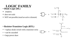
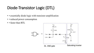
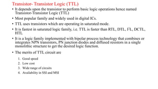
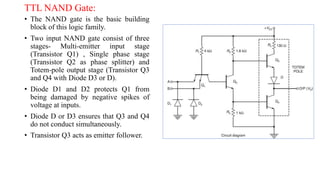
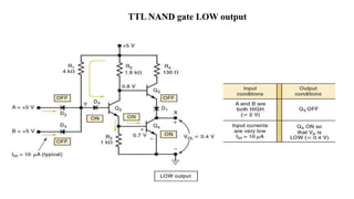
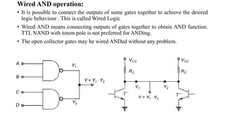
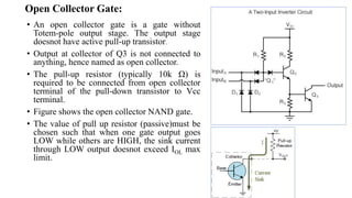
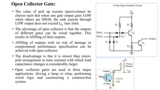
This document provides an introduction to different logic families including diode logic, resistor-transistor logic, diode-transistor logic, emitter-coupled logic, and transistor-transistor logic. It describes the characteristics and components of transistor-transistor logic gates including the TTL NAND gate structure with its input, phase splitter, and totem-pole output stages. It also discusses wired AND operation, open collector gates, and their advantages for interfacing logic families.
it covers topics Introduction
Classification of Logic Families
Important point
Level of Integration
Specification of Digital ICs
TTL Circuit
TTL NAND Gates
MOS/CMOS Circuits
CMOS NAND Gate
ECL Circuit
Comparison
Numbers of Digital ICs
Power point presentation on logical families.
A good presentation cover all topics.
For any other type of ppt's or pdf's to be created on demand contact -dhawalm8@gmail.com
mob. no-7023419969
Hierarchical Digital Twin of a Naval Power SystemKerry Sado
A hierarchical digital twin of a Naval DC power system has been developed and experimentally verified. Similar to other state-of-the-art digital twins, this technology creates a digital replica of the physical system executed in real-time or faster, which can modify hardware controls. However, its advantage stems from distributing computational efforts by utilizing a hierarchical structure composed of lower-level digital twin blocks and a higher-level system digital twin. Each digital twin block is associated with a physical subsystem of the hardware and communicates with a singular system digital twin, which creates a system-level response. By extracting information from each level of the hierarchy, power system controls of the hardware were reconfigured autonomously. This hierarchical digital twin development offers several advantages over other digital twins, particularly in the field of naval power systems. The hierarchical structure allows for greater computational efficiency and scalability while the ability to autonomously reconfigure hardware controls offers increased flexibility and responsiveness. The hierarchical decomposition and models utilized were well aligned with the physical twin, as indicated by the maximum deviations between the developed digital twin hierarchy and the hardware.
Final project report on grocery store management system..pdfKamal Acharya
In today’s fast-changing business environment, it’s extremely important to be able to respond to client needs in the most effective and timely manner. If your customers wish to see your business online and have instant access to your products or services.
Online Grocery Store is an e-commerce website, which retails various grocery products. This project allows viewing various products available enables registered users to purchase desired products instantly using Paytm, UPI payment processor (Instant Pay) and also can place order by using Cash on Delivery (Pay Later) option. This project provides an easy access to Administrators and Managers to view orders placed using Pay Later and Instant Pay options.
In order to develop an e-commerce website, a number of Technologies must be studied and understood. These include multi-tiered architecture, server and client-side scripting techniques, implementation technologies, programming language (such as PHP, HTML, CSS, JavaScript) and MySQL relational databases. This is a project with the objective to develop a basic website where a consumer is provided with a shopping cart website and also to know about the technologies used to develop such a website.
This document will discuss each of the underlying technologies to create and implement an e- commerce website.
1. Unit I:
Digital Logic Families
By
Dr. Anup Vibhute
Dr. D Y Patil Institute of Technology, Pimpri, Pune
2. Contents:
• Syllabus
• Logic families- Introduction
• Classification of Families
• Characteristics of Logic Families
• TTL families
• CMOS families
• Interfacing of TTL-CMOS
3. Syllabus:
Classification and Characteristics of digital Logic Families: -Speed, power
dissipation, figure of merit, fan in, fan out, current, voltage, noise immunity,
operating temperatures and power supply requirements.
TTL logic. Operation of TTL NAND gate, active pull up, wired AND, open
collector output, unconnected inputs. Tri-State logic.
CMOS logic: CMOS inverter, NAND, NOR gates, unconnected inputs, wired
logic, open drain output.
Interfacing CMOS and TTL and Data sheet specifications
Course Outcome:
CO1: Classify and characterize the digital logic families
• CO1.1 Classify the various Logic families on the basis of components
• CO1.2 Characterize the Logic families for various parameters.
6. LOGIC FAMILY
• Diode Logic (DL)
simplest;
does not scale
NOT not possible (need an active element)
• Resistor-Transistor Logic (RTL)
• • replace diode switch with a transistor switch
• • can be cascaded
• • large power draw
7. Diode-Transistor Logic (DTL)
• • essentially diode logic with transistor amplification
• • reduced power consumption
• • faster than RTL
8. ECL Emitter-Coupled Logic (ECL)
Based on BJT, but removes problems of delay time by preventing the transistors
from saturating
Very fast operation - propagation delays of 1ns or less
High power consumption, perhaps 60 mW/gate • Logic levels. “0”: –1.7V. “1”: –
0.8V
Such strange logic levels require extra effort when interfacing to TTL/CMOS
logic families. • low noise immunity of about 0.2-0.25 V
Used in some high speed specialist applications, but now largely replaced by high
speed CMOS
9. TTL Logic Families
• first introduced by in 1964 (Texas Instruments)
• TTL has shaped digital technology in many ways
• one of the most widely used families for small
and medium-scale devices – rarely used
for VLSI
• Standard TTL family (e.g. 7400) is obsolete
• Newer TTL families still used (e.g. 74ALS00)
• High energy consumption, but relatively
insensitive to electrostatic discharge (ESD)
• Distinct feature
10. Current Sourcing
• Current-sourcing action.
• When the output of gate 1 is HIGH, it supplies
current IIH to the input of gate 2.
• Which acts essentially as a resistance to ground.
• The output of gate 1 is acting as a source of
current for the gate 2 input.
11. Current Sinking
• Current-sinking action.
• Input circuitry of gate 2 is represented as a resistance tied to +VCC —the positive terminal of a power
supply.
• When gate 1 output goes LOW, current will flow from the input circuit of gate 2 back through the
output resistance of gate 1, to ground.
• Circuit output that drives the input of gate 2 must be able to sink a current, IIL , coming from that
input.
12. Transistor- Transistor Logic (TTL)
• It depends upon the transistor to perform basic logic operations hence named
Transistor-Transistor Logic (TTL)
• Most popular family and widely used in digital ICs.
• TTL uses transistors which are operating in saturated mode.
• It is fastest in saturated logic family, i.e. TTL is faster than RTL, DTL, I2L, DCTL,
HTL
• It is a logic family implemented with bipolar process technology that combines or
integrates NPN transistors, PN junction diodes and diffused resistors in a single
monolithic structure to get the desired logic function.
• The merits of TTL circuit are
1. Good speed
2. Low cost
3. Wide range of circuits
4. Availability in SSI and MSI
13. Transistor- Transistor Logic (TTL)
• Demerits are:
1. Tight Vcc Tolerance
2. Relatively high power consumption
3. Moderate packing density
4. Generation of noise spikes
5. Susceptibility to power transients
• TTL logic family have several subfamilies such as
• Standard TTL,
• High speed TTL,
• Low power TTL,
• Low power Schottky TTL,
• Advanced Schottky TTL,
• Advanced Low power Schottky TTL and
• Fast (F)TTL
14. TTL NAND Gate:
• The NAND gate is the basic building
block of this logic family.
• Two input NAND gate consist of three
stages- Multi-emitter input stage
(Transistor Q1) , Single phase stage
(Transistor Q2 as phase splitter) and
Totem-pole output stage (Transistor Q3
and Q4 with Diode D3 or D).
• Diode D1 and D2 protects Q1 from
being damaged by negative spikes of
voltage at inputs.
• Diode D or D3 ensures that Q3 and Q4
do not conduct simultaneously.
• Transistor Q3 acts as emitter follower.
15. TTL NAND Gate:
A B Vo Q1 Q2 Q3 Q4
0 (L) 0 (L) 1 (H) ON OFF ON OFF
0 1 1 ON OFF ON OFF
1 0 1 ON OFF ON OFF
1 1 0 OFF ON OFF ON
17. Q4 is performing a current-sinking action—
deriving its current from the input
current (IIL) of the load gate.
Q4 is often called the current-sinking
transistor or pull-down transistor because
it brings the output voltage down to its LOW
state.
TTL NAND gate LOW output..Cont
19. • A TTL output acts as a current source in the HIGH state.
Transistor Q3 is supplying the input current
(IIH) required
by Q1 of the load gate.
Q3 is often called the current-sourcing or pull-
up transistor.
In more modern TTL series,
the pull-up circuit is made
up of two transistors.
TTL NAND gate HIGH output…..Cont.
20. Totem Pole:
• Transistor Q3 & Q4 constitutes the
Totem-pole arrangement at the output
of NAND gate.
• At any time, only one of the transistors
is conducting, i.e., both cannot be
turned ON or OFF simultaneously and
its is ensured by diode D or D3.
21. Totem Pole:
• Advantages of Totem pole:
• It offers low output resistance in High & Low output
states.
• Because of low output impedance, any stray
capacitance at the output can be charged or
discharged rapidly allowing to change output from
one state to other quickly.
• When output is in low state, transistor Q4 need to
conduct large current through R3. Inclusion of Q3
and D keeps circuit power dissipation low.
22. Totem Pole:
• Disadvantages of Totem-pole:
• Switch off action of Q4 is slower than the switch-off
action of Q3. Because of this for fraction of time,
few nanoseconds both the transistors are ON, which
results in drawing heavy current from supply.
• TTL-pole outputs cannot be wire ANDed, i.e.
outputs of a number of gates cannot be tied together
to obtain AND operation.
• When two totem poles are wired together. with the
output of one gale high and the output of the second
gate low, the excessive amount of current drawn can
produce enough heat to damage the transistors in the
circuit.
23. Wired AND operation:
• It is possible to connect the outputs of some gates together to achieve the desired
logic behaviour . This is called Wired Logic
• Wired AND means connecting outputs of gates together to obtain AND function.
TTL NAND with totem pole is not preferred for ANDing.
• The open collector gates may be wired ANDed without any problem.
24. Wired AND operation:
• AND gate operation can be achieved
by using additional NAND gates as
shown in figure b
• The same logic can be performed
simply tying out the outputs of
NAND gates as shown in figure a.
25. Open Collector Gate:
• An open collector gate is a gate without
Totem-pole output stage. The output stage
doesnot have active pull-up transistor.
• Output at collector of Q3 is not connected to
anything, hence named as open collector.
• The pull-up resistor (typically 10k Ω) is
required to be connected from open collector
terminal of the pull-down transistor to Vcc
terminal.
• Figure shows the open collector NAND gate.
• The value of pull up resistor (passive)must be
chosen such that when one gate output goes
LOW while others are HIGH, the sink current
through LOW output doesnot exceed IOL max
limit.
26. Open Collector Gate:
• The value of pull up resistor (passive)must be
chosen such that when one gate output goes LOW
while others are HIGH, the sink current through
LOW output does not exceed IOL max limit.
• The advantage of open collector is that the outputs
of different gates can be wired together. This
results in ANDing of their outputs.
• ANDing of outputs with no risk of damage or
compromised performance specification can be
achieved with open collector.
• The disadvantage is that it is slower than totem-
pole arrangement as time constant with which load
capacitance changes is considerably larger.
• Open -collector gates are used in three major
applications: driving a lamp or relay, performing
wired logic and constructing a common-bus
system.