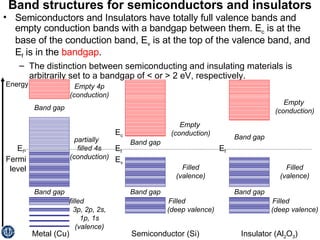
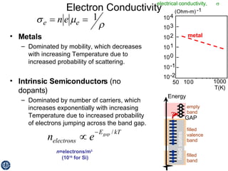
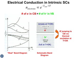
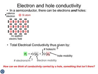
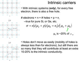
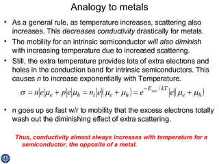
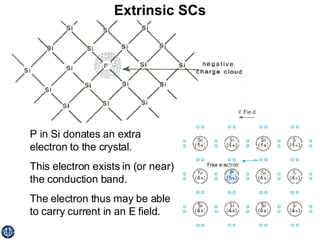
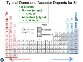
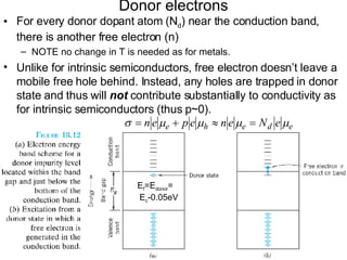
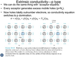
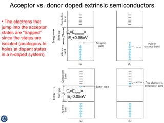
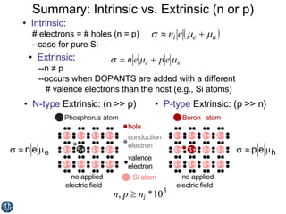
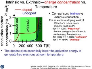
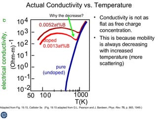
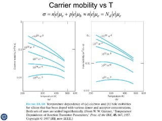
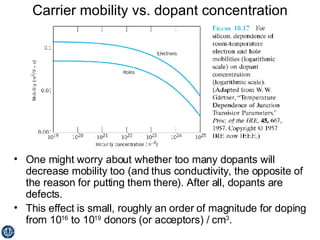
Today’s objectives-  Semiconductors and Integrated Circuits Draw band diagrams for metals, insulators, intrinsic semiconductor, and n and p type doped semiconductors, including E c , E f , and E v . How does conductivity change as a function of temperature for metals and intrinsic semiconductors. What about for extrinsic (doped) semiconductors?  What are common n and p type dopants? What is the appropriate conductivity equation for intrinsic, n, and p type semiconductors. How does the concentration of free charges change with temperature and doping (for intrinsic and extrinsic semiconductors)? How does mobility change with temperature  and doping?
Semiconductor Industry in 2003 The semiconductor business: $166B. 10 18  transistors produced during the year. US semiconductor industry:  $80B.  $13B reinvested in research, $10B in equipment. 226 000 jobs in US alone. http://www.infras.com/Tutorial/sld001.htm
Typical Semiconductors GaAs ZnS (Zinc Blende) Structure 4 Ga atoms at (0,0,0)+ FCC translations 4 As atoms at ( ¼,¼,¼)+FCC translations Bonding: covalent, partially ionic Silicon Diamond Cubic Structure 4 atoms at (0,0,0)+ FCC translations 4 atoms at ( ¼,¼,¼)+FCC translations Bonding: covalent
Band structures for semiconductors and insulators Semiconductors and Insulators have totally full valence bands and empty conduction bands with a bandgap between them. E c  is at the base of the conduction band, E v  is at the top of the valence band, and E f  is in the  bandgap . The distinction between semiconducting and insulating materials is arbitrarily set to a bandgap of < or > 2 eV, respectively. E f , Fermi level Metal (Cu) partially  filled 4s (conduction) filled  3p, 2p, 2s, 1p, 1s (valence) Empty 4p (conduction) Band gap Band gap Energy Filled  (deep valence) E f Insulator (Al 2 O 3 ) Filled (valence) Empty  (conduction) Band gap Band gap Filled  (deep valence) E f Semiconductor (Si) Filled (valence) Empty  (conduction) Band gap Band gap E c E v
Electron Conductivity Metals Dominated by mobility, which decreases with increasing Temperature due to increased probability of scattering. Intrinsic Semiconductors  (no dopants) Dominated by number of carriers, which increases exponentially with increasing Temperature due to increased probability of electrons jumping across the band gap. n =electrons/m 3   (10 16  for Si) metal
Electrical Conduction in Intrinsic SCs  Schematic Band Diagram “ Real” Band Diagram (empty at T=OK) (full at T=OK) h + e - # of e -  in CB  =  # of h +  in VB e -   jumping to CB via thermal excitation at T>OK
Electron and hole conductivity How can we think of conductivity carried by a hole, something that isn’t there? •  Total Electrical Conductivity thus given by: # electrons/m 3 electron mobility # holes/m 3 hole mobility •  In a semiconductor, there can be electrons  and  holes:
Intrinsic carriers With intrinsic systems ( only ), for every free electron, there is also a free hole. # electrons = n = # holes = p = n i --true for pure Si, or Ge, etc. Holes don’t move as easily (mobility of holes is always less than for electrons), but still there are so many that they will contribute at least an extra 10-20% to the intrinsic conductivity. μ h  is  ~ 20% of  μ e
Analogy to metals As a general rule, as temperature increases, scattering also increases. This  decreases conductivity  drastically for metals. The mobility for an intrinsic semiconductor  will also diminish  with increasing temperature   due to increased scattering.  Still, the extra temperature provides lots of extra electrons and holes in the conduction band for intrinsic semiconductors. This causes  n  to increase exponentially with Temperature. n goes up so fast w/r to mobility that the excess electrons totally wash out the diminishing effect of extra scattering. Thus, conductivity almost always increases with temperature for a semiconductor, the opposite of a metal.
Extrinsic SCs P in Si donates an extra electron to the crystal. This electron exists in (or near) the conduction band. The electron thus may be able to carry current in an E field.
Typical Donor and Acceptor Dopants for Si For Silicon: Donors (n type): P, As, Sb Acceptors (p type): B, Al, Ga, In
Donor electrons For every donor dopant atom (N d ) near the conduction band, there is another free electron (n) NOTE no change in T is needed as for metals. Unlike for intrinsic semiconductors, free electron doesn’t leave a mobile free hole behind. Instead, any holes are trapped in donor state and thus will  not  contribute substantially to conductivity as for intrinsic semiconductors (thus p ~ 0). E f =E donor =  E c -0.05eV
Extrinsic conductivity—p type We can do the same thing with “acceptor dopants.”  Every acceptor generates excess mobile holes (p=N a ). Now holes totally outnumber electrons, so conductivity equation switches to p domination.
Acceptor vs. donor doped extrinsic semiconductors E f =E donor =  E c -0.05eV E f =E acceptor =  E v +0.05eV The electrons that jump into the acceptor states are “trapped” since the states are isolated (analogous to holes at dopant states in a n-doped system).
Summary: Intrinsic vs. Extrinsic (n or p) •  Intrinsic : # electrons = # holes (n = p) --case for pure Si •  Extrinsic : --n ≠ p --occurs when DOPANTS are added with a different # valence electrons than the host (e.g., Si atoms) •  N-type  Extrinsic: (n >> p) •  P-type  Extrinsic: (p >> n)
Intrinsic vs. Extrinsic— charge concentration  vs. Temperature The dopant sites essentially lower the activation energy to generate free electrons at room temperature. •  Comparison:   intrinsic  vs extrinsic  conduction... For an extrinsic doping level of: 10 21 /m 3  of a n-type donor impurity (such as P). --for T < 100K:  &quot; freeze-out” thermal energy only sufficient to excite a very few electrons. --for 150K < T < 450K:  &quot;extrinsic&quot; --for T >> 450K:  &quot;intrinsic&quot; Adapted from Fig. 18.16,  Callister 6e .  (Fig. 18.16 from S.M. Sze,  Semiconductor Devices, Physics, and Technology , Bell Telephone Laboratories, Inc., 1985.)
Actual Conductivity vs. Temperature Conductivity is not as flat as free charge concentration. This is because mobility is always decreasing with increased temperature (more scattering) Adapted from Fig. 19.15,  Callister 5e .  (Fig. 19.15 adapted from G.L. Pearson and J. Bardeen,  Phys. Rev.  75 , p. 865, 1949.) Why the decrease?
Carrier mobility vs T
Carrier mobility vs. dopant concentration One might worry about whether too many dopants will decrease mobility too (and thus conductivity, the opposite of the reason for putting them there). After all, dopants are defects. This effect is small, roughly an order of magnitude for doping from 10 16  to 10 19  donors (or acceptors) / cm 3 .
SUMMARY Draw band diagrams for metals, insulators, intrinsic semiconductor, and n and p type doped semiconductors, including E c , E f , and E v . How does conductivity change as a function of temperature for metals and intrinsic semiconductors. What about for extrinsic (doped) semiconductors?  What are common n and p type dopants? What is the appropriate conductivity equation for intrinsic, n, and p type semiconductors. How does the concentration of free charges change with temperature and doping (for intrinsic and extrinsic semiconductors)? How does mobility change with temperature and doping?

Lecture 15

  • 1.
    Today’s objectives- Semiconductors and Integrated Circuits Draw band diagrams for metals, insulators, intrinsic semiconductor, and n and p type doped semiconductors, including E c , E f , and E v . How does conductivity change as a function of temperature for metals and intrinsic semiconductors. What about for extrinsic (doped) semiconductors? What are common n and p type dopants? What is the appropriate conductivity equation for intrinsic, n, and p type semiconductors. How does the concentration of free charges change with temperature and doping (for intrinsic and extrinsic semiconductors)? How does mobility change with temperature and doping?
  • 2.
    Semiconductor Industry in2003 The semiconductor business: $166B. 10 18 transistors produced during the year. US semiconductor industry: $80B. $13B reinvested in research, $10B in equipment. 226 000 jobs in US alone. http://www.infras.com/Tutorial/sld001.htm
  • 3.
    Typical Semiconductors GaAsZnS (Zinc Blende) Structure 4 Ga atoms at (0,0,0)+ FCC translations 4 As atoms at ( ¼,¼,¼)+FCC translations Bonding: covalent, partially ionic Silicon Diamond Cubic Structure 4 atoms at (0,0,0)+ FCC translations 4 atoms at ( ¼,¼,¼)+FCC translations Bonding: covalent
  • 4.
    Band structures forsemiconductors and insulators Semiconductors and Insulators have totally full valence bands and empty conduction bands with a bandgap between them. E c is at the base of the conduction band, E v is at the top of the valence band, and E f is in the bandgap . The distinction between semiconducting and insulating materials is arbitrarily set to a bandgap of < or > 2 eV, respectively. E f , Fermi level Metal (Cu) partially filled 4s (conduction) filled 3p, 2p, 2s, 1p, 1s (valence) Empty 4p (conduction) Band gap Band gap Energy Filled (deep valence) E f Insulator (Al 2 O 3 ) Filled (valence) Empty (conduction) Band gap Band gap Filled (deep valence) E f Semiconductor (Si) Filled (valence) Empty (conduction) Band gap Band gap E c E v
  • 5.
    Electron Conductivity MetalsDominated by mobility, which decreases with increasing Temperature due to increased probability of scattering. Intrinsic Semiconductors (no dopants) Dominated by number of carriers, which increases exponentially with increasing Temperature due to increased probability of electrons jumping across the band gap. n =electrons/m 3 (10 16 for Si) metal
  • 6.
    Electrical Conduction inIntrinsic SCs Schematic Band Diagram “ Real” Band Diagram (empty at T=OK) (full at T=OK) h + e - # of e - in CB = # of h + in VB e - jumping to CB via thermal excitation at T>OK
  • 7.
    Electron and holeconductivity How can we think of conductivity carried by a hole, something that isn’t there? • Total Electrical Conductivity thus given by: # electrons/m 3 electron mobility # holes/m 3 hole mobility • In a semiconductor, there can be electrons and holes:
  • 8.
    Intrinsic carriers Withintrinsic systems ( only ), for every free electron, there is also a free hole. # electrons = n = # holes = p = n i --true for pure Si, or Ge, etc. Holes don’t move as easily (mobility of holes is always less than for electrons), but still there are so many that they will contribute at least an extra 10-20% to the intrinsic conductivity. μ h is ~ 20% of μ e
  • 9.
    Analogy to metalsAs a general rule, as temperature increases, scattering also increases. This decreases conductivity drastically for metals. The mobility for an intrinsic semiconductor will also diminish with increasing temperature due to increased scattering. Still, the extra temperature provides lots of extra electrons and holes in the conduction band for intrinsic semiconductors. This causes n to increase exponentially with Temperature. n goes up so fast w/r to mobility that the excess electrons totally wash out the diminishing effect of extra scattering. Thus, conductivity almost always increases with temperature for a semiconductor, the opposite of a metal.
  • 10.
    Extrinsic SCs Pin Si donates an extra electron to the crystal. This electron exists in (or near) the conduction band. The electron thus may be able to carry current in an E field.
  • 11.
    Typical Donor andAcceptor Dopants for Si For Silicon: Donors (n type): P, As, Sb Acceptors (p type): B, Al, Ga, In
  • 12.
    Donor electrons Forevery donor dopant atom (N d ) near the conduction band, there is another free electron (n) NOTE no change in T is needed as for metals. Unlike for intrinsic semiconductors, free electron doesn’t leave a mobile free hole behind. Instead, any holes are trapped in donor state and thus will not contribute substantially to conductivity as for intrinsic semiconductors (thus p ~ 0). E f =E donor = E c -0.05eV
  • 13.
    Extrinsic conductivity—p typeWe can do the same thing with “acceptor dopants.” Every acceptor generates excess mobile holes (p=N a ). Now holes totally outnumber electrons, so conductivity equation switches to p domination.
  • 14.
    Acceptor vs. donordoped extrinsic semiconductors E f =E donor = E c -0.05eV E f =E acceptor = E v +0.05eV The electrons that jump into the acceptor states are “trapped” since the states are isolated (analogous to holes at dopant states in a n-doped system).
  • 15.
    Summary: Intrinsic vs.Extrinsic (n or p) • Intrinsic : # electrons = # holes (n = p) --case for pure Si • Extrinsic : --n ≠ p --occurs when DOPANTS are added with a different # valence electrons than the host (e.g., Si atoms) • N-type Extrinsic: (n >> p) • P-type Extrinsic: (p >> n)
  • 16.
    Intrinsic vs. Extrinsic—charge concentration vs. Temperature The dopant sites essentially lower the activation energy to generate free electrons at room temperature. • Comparison: intrinsic vs extrinsic conduction... For an extrinsic doping level of: 10 21 /m 3 of a n-type donor impurity (such as P). --for T < 100K: &quot; freeze-out” thermal energy only sufficient to excite a very few electrons. --for 150K < T < 450K: &quot;extrinsic&quot; --for T >> 450K: &quot;intrinsic&quot; Adapted from Fig. 18.16, Callister 6e . (Fig. 18.16 from S.M. Sze, Semiconductor Devices, Physics, and Technology , Bell Telephone Laboratories, Inc., 1985.)
  • 17.
    Actual Conductivity vs.Temperature Conductivity is not as flat as free charge concentration. This is because mobility is always decreasing with increased temperature (more scattering) Adapted from Fig. 19.15, Callister 5e . (Fig. 19.15 adapted from G.L. Pearson and J. Bardeen, Phys. Rev. 75 , p. 865, 1949.) Why the decrease?
  • 18.
  • 19.
    Carrier mobility vs.dopant concentration One might worry about whether too many dopants will decrease mobility too (and thus conductivity, the opposite of the reason for putting them there). After all, dopants are defects. This effect is small, roughly an order of magnitude for doping from 10 16 to 10 19 donors (or acceptors) / cm 3 .
  • 20.
    SUMMARY Draw banddiagrams for metals, insulators, intrinsic semiconductor, and n and p type doped semiconductors, including E c , E f , and E v . How does conductivity change as a function of temperature for metals and intrinsic semiconductors. What about for extrinsic (doped) semiconductors? What are common n and p type dopants? What is the appropriate conductivity equation for intrinsic, n, and p type semiconductors. How does the concentration of free charges change with temperature and doping (for intrinsic and extrinsic semiconductors)? How does mobility change with temperature and doping?