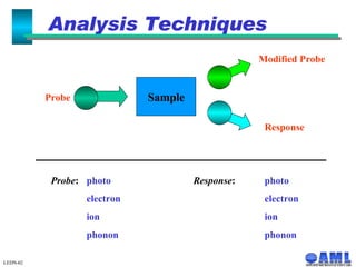
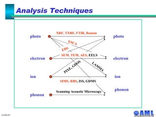
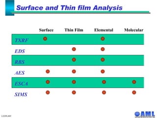
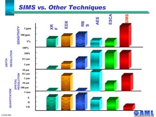
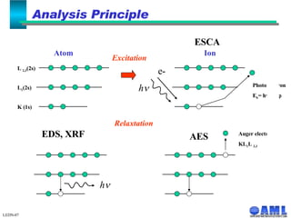
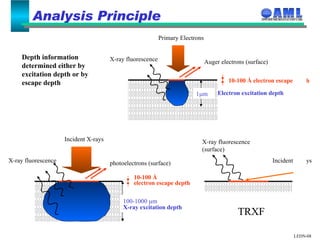
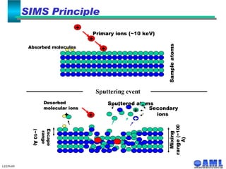
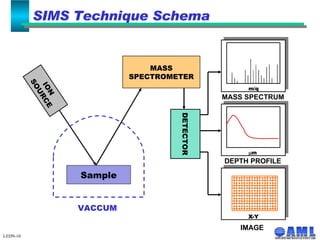
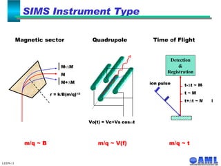
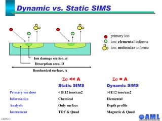
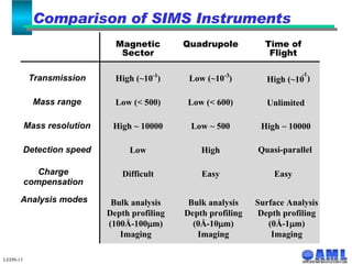
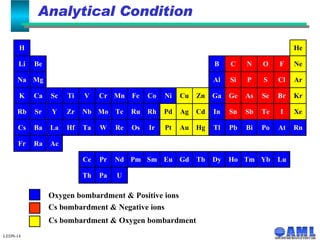
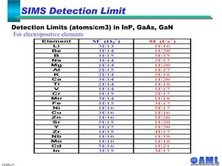
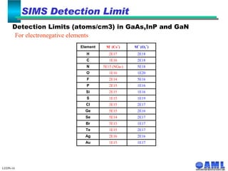
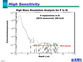
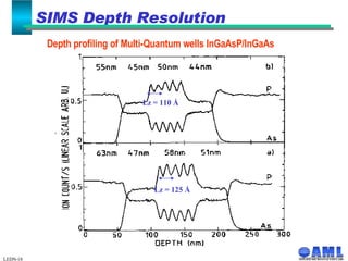
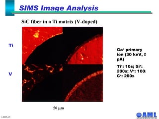
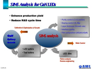
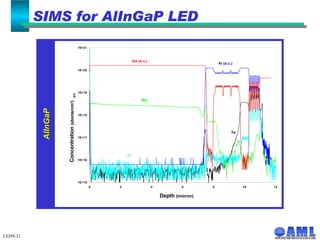
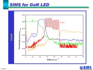
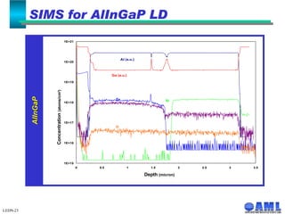
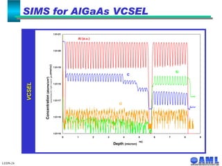
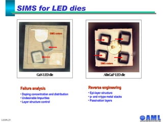
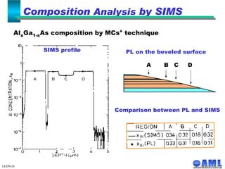
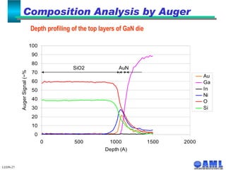
LEDN-02 Analysis Techniques Sample Probe Response Modified Probe Probe : photo Response : photo electron electron ion ion phonon phonon
Analysis Techniques phonon photo photo XRF, TXRF, FTIR, Raman electron electron ion ion phonon SIMS, RBS , ISS, GDMS ESCA EDS PIXE, GDOS SEM, TEM, AES,  EELS LAMMA LEDN-03 Scanning Acoustic Microscopy
LEDN-004 Analysis Techniques Elemental   Molecular Surface  ( <10 Å) Thin film  ( <100 Å - 1  m) Bulk ( > 10  m) Types of information provided by chemical analysis
LEDN-005 Surface and Thin film Analysis    Surface  Thin Film  Elemental  Molecular TXRF EDS RBS  AES ESCA SIMS
100% 100 ppm 1% 1 ppm XRF ESCA AES RBS SIMS EDX 100Å 10 µm 0.1 µm 1 µm 1 µm 0.1 µm 10 µm 100 µm 1 mm VD D E SENSITIVITY SPATIAL RESOLUTION QUANTITATION DEPTH  RESOLUTION LEDN-006 SIMS vs. Other Techniques
LEDN-07 Analysis Principle  Excitation Photoelectron E b = h  -E k -  Relaxtation ESCA EDS, XRF AES Auger electron KL 1 L  2,3 K (1s) L 1 (2s) L  2,3 (2s) Atom Ion e- h  h 
LEDN-08 Analysis Principle  X-ray fluorescence (surface) Incident X-rays TRXF Depth information determined either by excitation depth or by escape depth 10-100 Å electron escape depth 1  m Electron excitation depth Auger electrons (surface) X-ray fluorescence Primary Electrons 10-100 Å  electron escape depth 100-1000   m   X-ray excitation depth photoelectrons (surface) X-ray fluorescence Incident X-rays
LEDN-09 Absorbed molecules Sputtered atoms SIMS Principle Sputtering event + + + Primary ions (~10 keV) Sample atoms + + - + + Secondary ions  Mixing range  (~100 Å) Escape range (~10 Å) Desorbed molecular ions
LEDN-10 SIMS Technique Schema ION SOURCE Sample MASS SPECTROMETER DETECTOR MASS SPECTRUM  m DEPTH PROFILE X-Y IMAGE VACCUM m/q
Magnetic sector   Quadrupole   Time of Flight LEDN-11 SIMS Instrument Type r = k/B(m/q) 1/2 M-  M M M+  M Vo(t) = Vc+Vs cos  t t-  t ~ M-  M t ~ M t+  t ~ M+  M ion pulse Detection & Registration m/q ~ B     m/q ~ V(f)  m/q ~ t
   <<  A      =  A  Static SIMS Dynamic SIMS Primary ion dose <1E12 ions/cm2 >1E12 ions/cm2 Information Chemical Elemental Analysis Only surface Depth profile Instrument TOF & Quad Magnetic & Quad Ion damage section,   Desorption area, D Bombarded surface, A LEDN-12 Dynamic vs. Static SIMS primary ion ion:  elementa l information ion:  molecular  information
LEDN-13 Comparison of SIMS Instruments   Magnetic Sector Quadrupole Time of Flight Transmission High (~10 -1 ) Low (~10 -3 ) High (~10  -1 ) Mass range Low (< 500) Low (< 600) Unlimited Mass resolution High ~ 10000 Low ~ 500 High ~ 10000 Detection speed Low High Quasi-parallel Charge compensation Difficult Easy Easy Analysis modes Bulk analysis Depth profiling (100Å-100  m) Imaging Bulk analysis Depth profiling (0Å-10  m) Imaging Surface Analysis Depth profiling (0Å-1  m) Imaging
Analytical Condition LEDN-14 Oxygen bombardment & Positive ions Cs bombardment & Negative ions Cs bombardment & Oxygen bombardment
LEDN-15 Detection Limits (atoms/cm3) in InP, GaAs, GaN For electropositive elements   SIMS Detection Limit
LEDN-16 Detection Limits (atoms/cm3) in GaAs,InP and GaN For electronegative elements   SIMS Detection Limit
Depth (  m) 1E13 at/cm3 LEDN-17 High Mass Resolution Analysis for P in Si  High Sensitivity Concentration(at/cm3) P implantation in Si (2E12 atoms/cm2, 300 keV)
LEDN-18 Depth profiling of Multi-Quantum wells InGaAsP/InGaAs SIMS Depth Resolution Lz = 110 Å Lz = 125 Å
SiC fiber in a Ti matrix (V-doped)   LEDN-19 Ti C Si V 50   m Ga +  primary ion (30 keV, 50 pA) Ti + : 10s; Si + : 200s; V + : 100s; C + : 200s SIMS Image Analysis
SIMS Analysis for GaN LEDs LEDN-20 Enhance production yield Wafer Control LED wafers Test wafers Purity control (C,H,O,metals) Doping control (Si, Mg) Layer thickness (Growth rate) Interface quality Film composition (AlGaN,InGaN) SIMS analysis   Calibration &   Optimization of Growth GaN Epitaxy Growth Failure analysis Reverse engineering LED  dies Reduce R&D cycle time
SIMS for AlInGaP LED LEDN-21 Depth  (micron) Concentration  (atoms/cm 3 ) AlInGaP
LEDN-22 SIMS for GaN LED Depth  (micron) Concentration  (atoms/cm 3 ) InGaN
SIMS for AlInGaP LD LEDN-23 Depth  (micron) Concentration  (atoms/cm 3 ) AlInGaP
SIMS for AlGaAs VCSEL LEDN-24 Depth  (micron) Concentration  (atoms/cm 3 ) VCSEL
SIMS for LED dies LEDN-25 GaN LED die SIMS craters AlInGaP LED die  SIMS craters Doping concentration and distribution Undesirable Impurities Layer structure control Failure analysis Epi-layer structure p- and n-type metal stacks Passivation layers Reverse engineering
PL on the beveled surface SIMS profile Comparison between PL and SIMS LEDN-26 Composition  Analysis  by SIMS Al x Ga 1-x As composition by MCs +  technique A  B  C  D
Composition Analysis by Auger LEDN-27 Depth profiling of the top layers of GaN die

Surface Analysis

  • 1.
    LEDN-02 Analysis TechniquesSample Probe Response Modified Probe Probe : photo Response : photo electron electron ion ion phonon phonon
  • 2.
    Analysis Techniques phononphoto photo XRF, TXRF, FTIR, Raman electron electron ion ion phonon SIMS, RBS , ISS, GDMS ESCA EDS PIXE, GDOS SEM, TEM, AES, EELS LAMMA LEDN-03 Scanning Acoustic Microscopy
  • 3.
    LEDN-004 Analysis TechniquesElemental Molecular Surface ( <10 Å) Thin film ( <100 Å - 1  m) Bulk ( > 10  m) Types of information provided by chemical analysis
  • 4.
    LEDN-005 Surface andThin film Analysis Surface Thin Film Elemental Molecular TXRF EDS RBS AES ESCA SIMS
  • 5.
    100% 100 ppm1% 1 ppm XRF ESCA AES RBS SIMS EDX 100Å 10 µm 0.1 µm 1 µm 1 µm 0.1 µm 10 µm 100 µm 1 mm VD D E SENSITIVITY SPATIAL RESOLUTION QUANTITATION DEPTH RESOLUTION LEDN-006 SIMS vs. Other Techniques
  • 6.
    LEDN-07 Analysis Principle Excitation Photoelectron E b = h  -E k -  Relaxtation ESCA EDS, XRF AES Auger electron KL 1 L 2,3 K (1s) L 1 (2s) L 2,3 (2s) Atom Ion e- h  h 
  • 7.
    LEDN-08 Analysis Principle X-ray fluorescence (surface) Incident X-rays TRXF Depth information determined either by excitation depth or by escape depth 10-100 Å electron escape depth 1  m Electron excitation depth Auger electrons (surface) X-ray fluorescence Primary Electrons 10-100 Å electron escape depth 100-1000  m X-ray excitation depth photoelectrons (surface) X-ray fluorescence Incident X-rays
  • 8.
    LEDN-09 Absorbed moleculesSputtered atoms SIMS Principle Sputtering event + + + Primary ions (~10 keV) Sample atoms + + - + + Secondary ions Mixing range (~100 Å) Escape range (~10 Å) Desorbed molecular ions
  • 9.
    LEDN-10 SIMS TechniqueSchema ION SOURCE Sample MASS SPECTROMETER DETECTOR MASS SPECTRUM  m DEPTH PROFILE X-Y IMAGE VACCUM m/q
  • 10.
    Magnetic sector Quadrupole Time of Flight LEDN-11 SIMS Instrument Type r = k/B(m/q) 1/2 M-  M M M+  M Vo(t) = Vc+Vs cos  t t-  t ~ M-  M t ~ M t+  t ~ M+  M ion pulse Detection & Registration m/q ~ B m/q ~ V(f) m/q ~ t
  • 11.
     << A  = A Static SIMS Dynamic SIMS Primary ion dose <1E12 ions/cm2 >1E12 ions/cm2 Information Chemical Elemental Analysis Only surface Depth profile Instrument TOF & Quad Magnetic & Quad Ion damage section,  Desorption area, D Bombarded surface, A LEDN-12 Dynamic vs. Static SIMS primary ion ion: elementa l information ion: molecular information
  • 12.
    LEDN-13 Comparison ofSIMS Instruments Magnetic Sector Quadrupole Time of Flight Transmission High (~10 -1 ) Low (~10 -3 ) High (~10 -1 ) Mass range Low (< 500) Low (< 600) Unlimited Mass resolution High ~ 10000 Low ~ 500 High ~ 10000 Detection speed Low High Quasi-parallel Charge compensation Difficult Easy Easy Analysis modes Bulk analysis Depth profiling (100Å-100  m) Imaging Bulk analysis Depth profiling (0Å-10  m) Imaging Surface Analysis Depth profiling (0Å-1  m) Imaging
  • 13.
    Analytical Condition LEDN-14Oxygen bombardment & Positive ions Cs bombardment & Negative ions Cs bombardment & Oxygen bombardment
  • 14.
    LEDN-15 Detection Limits(atoms/cm3) in InP, GaAs, GaN For electropositive elements SIMS Detection Limit
  • 15.
    LEDN-16 Detection Limits(atoms/cm3) in GaAs,InP and GaN For electronegative elements SIMS Detection Limit
  • 16.
    Depth ( m) 1E13 at/cm3 LEDN-17 High Mass Resolution Analysis for P in Si High Sensitivity Concentration(at/cm3) P implantation in Si (2E12 atoms/cm2, 300 keV)
  • 17.
    LEDN-18 Depth profilingof Multi-Quantum wells InGaAsP/InGaAs SIMS Depth Resolution Lz = 110 Å Lz = 125 Å
  • 18.
    SiC fiber ina Ti matrix (V-doped) LEDN-19 Ti C Si V 50  m Ga + primary ion (30 keV, 50 pA) Ti + : 10s; Si + : 200s; V + : 100s; C + : 200s SIMS Image Analysis
  • 19.
    SIMS Analysis forGaN LEDs LEDN-20 Enhance production yield Wafer Control LED wafers Test wafers Purity control (C,H,O,metals) Doping control (Si, Mg) Layer thickness (Growth rate) Interface quality Film composition (AlGaN,InGaN) SIMS analysis Calibration & Optimization of Growth GaN Epitaxy Growth Failure analysis Reverse engineering LED dies Reduce R&D cycle time
  • 20.
    SIMS for AlInGaPLED LEDN-21 Depth (micron) Concentration (atoms/cm 3 ) AlInGaP
  • 21.
    LEDN-22 SIMS forGaN LED Depth (micron) Concentration (atoms/cm 3 ) InGaN
  • 22.
    SIMS for AlInGaPLD LEDN-23 Depth (micron) Concentration (atoms/cm 3 ) AlInGaP
  • 23.
    SIMS for AlGaAsVCSEL LEDN-24 Depth (micron) Concentration (atoms/cm 3 ) VCSEL
  • 24.
    SIMS for LEDdies LEDN-25 GaN LED die SIMS craters AlInGaP LED die SIMS craters Doping concentration and distribution Undesirable Impurities Layer structure control Failure analysis Epi-layer structure p- and n-type metal stacks Passivation layers Reverse engineering
  • 25.
    PL on thebeveled surface SIMS profile Comparison between PL and SIMS LEDN-26 Composition Analysis by SIMS Al x Ga 1-x As composition by MCs + technique A B C D
  • 26.
    Composition Analysis byAuger LEDN-27 Depth profiling of the top layers of GaN die