Download as PDF, PPTX
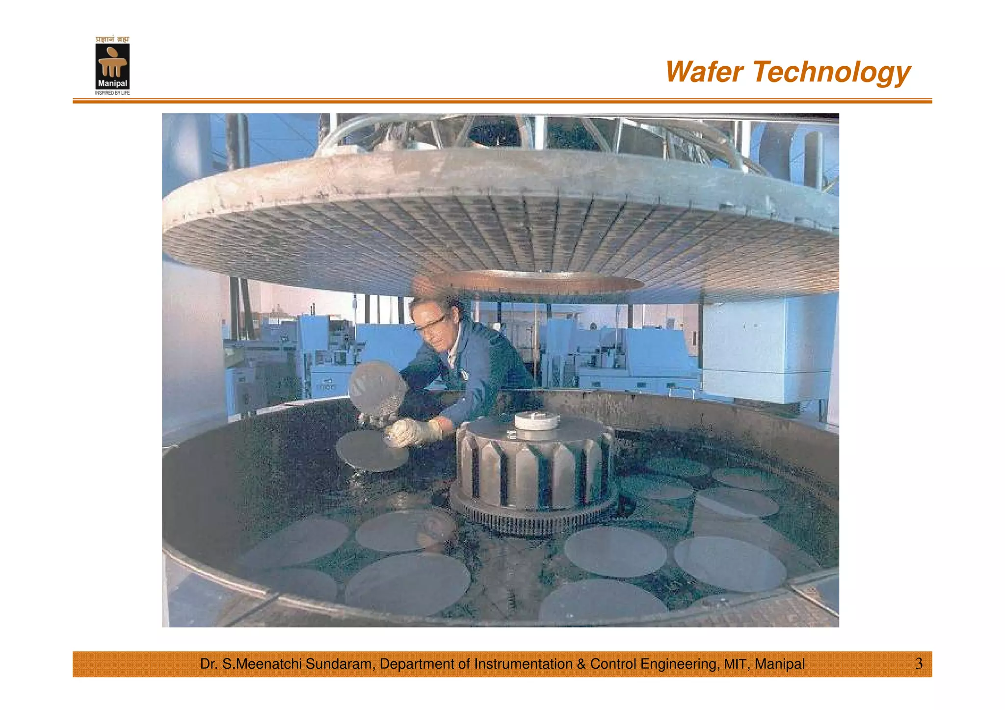
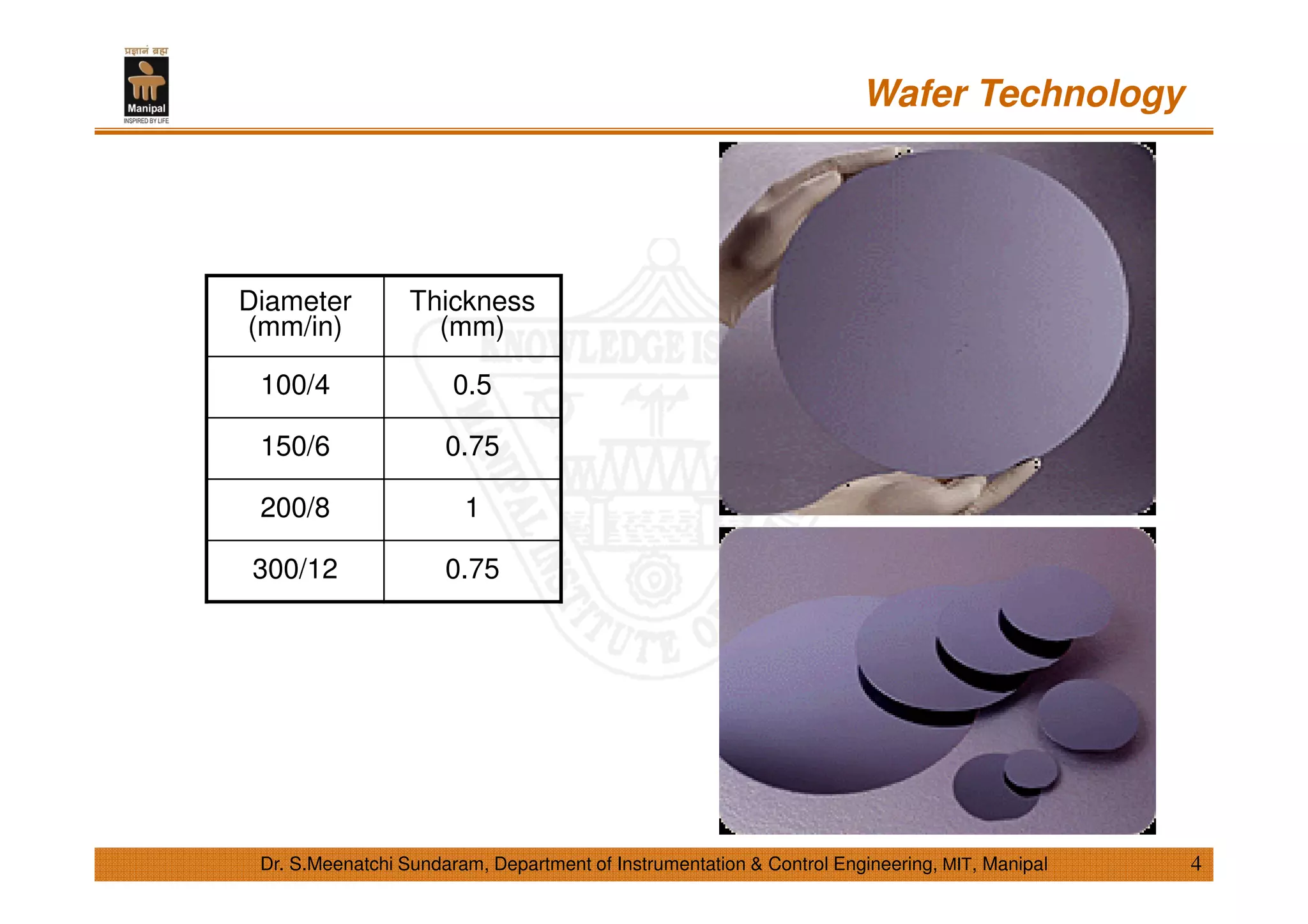
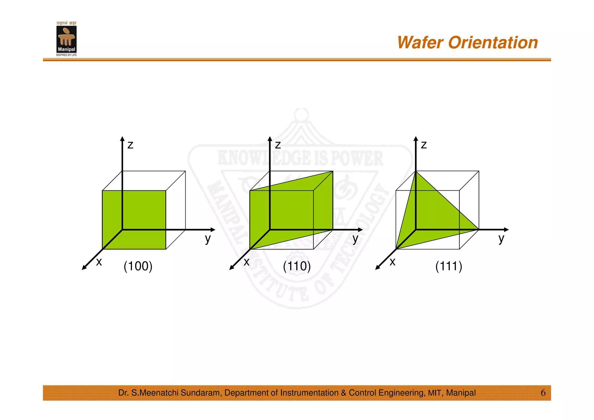
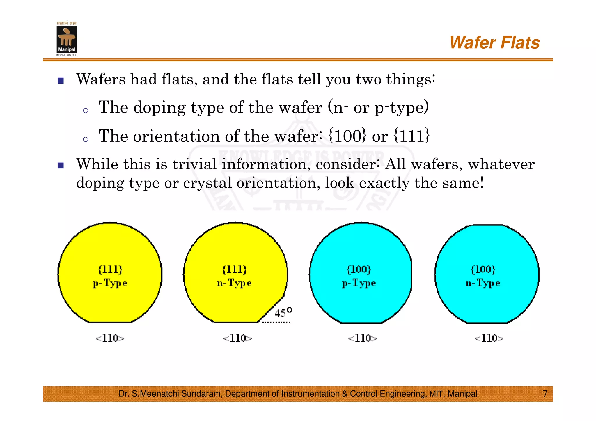
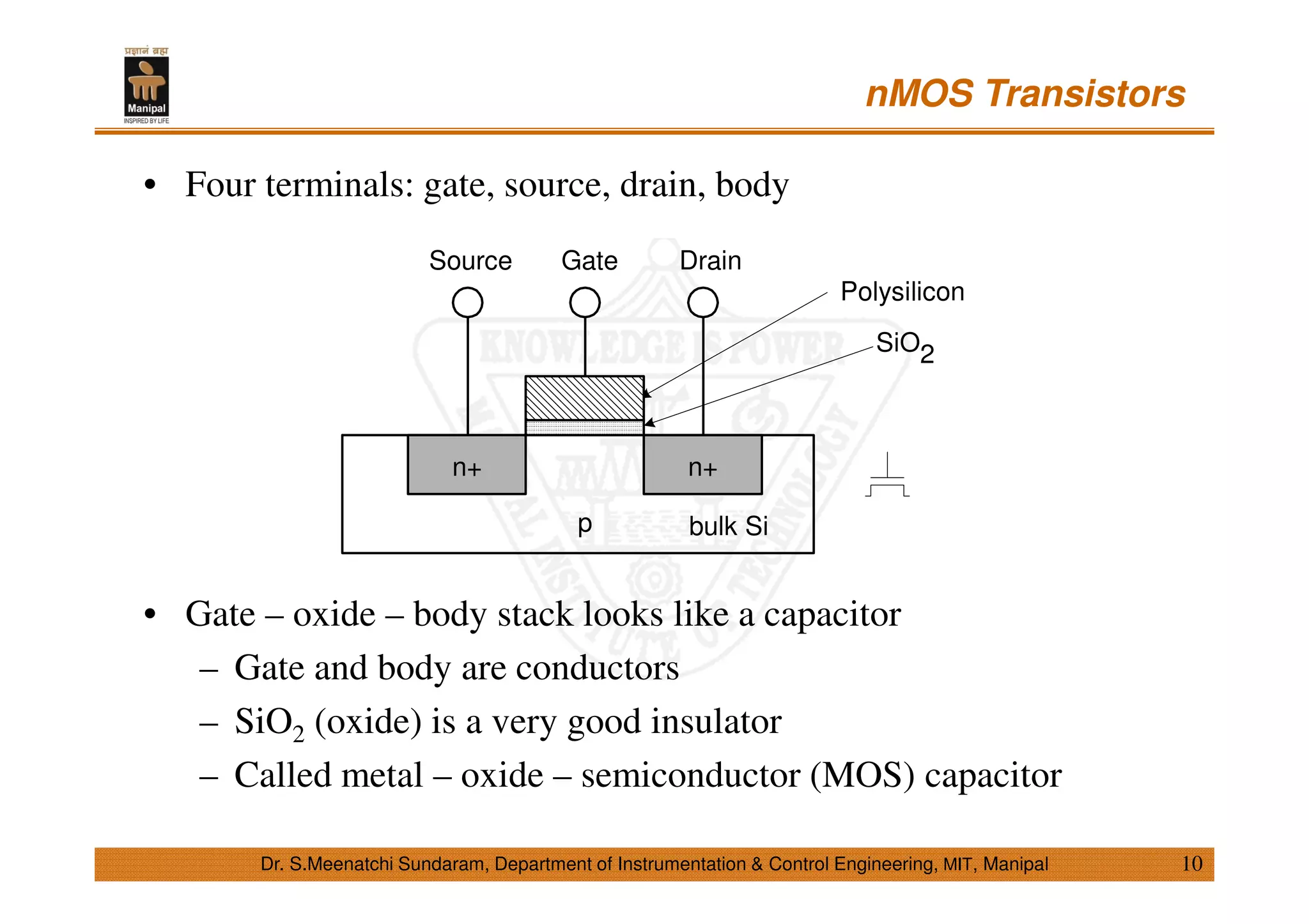
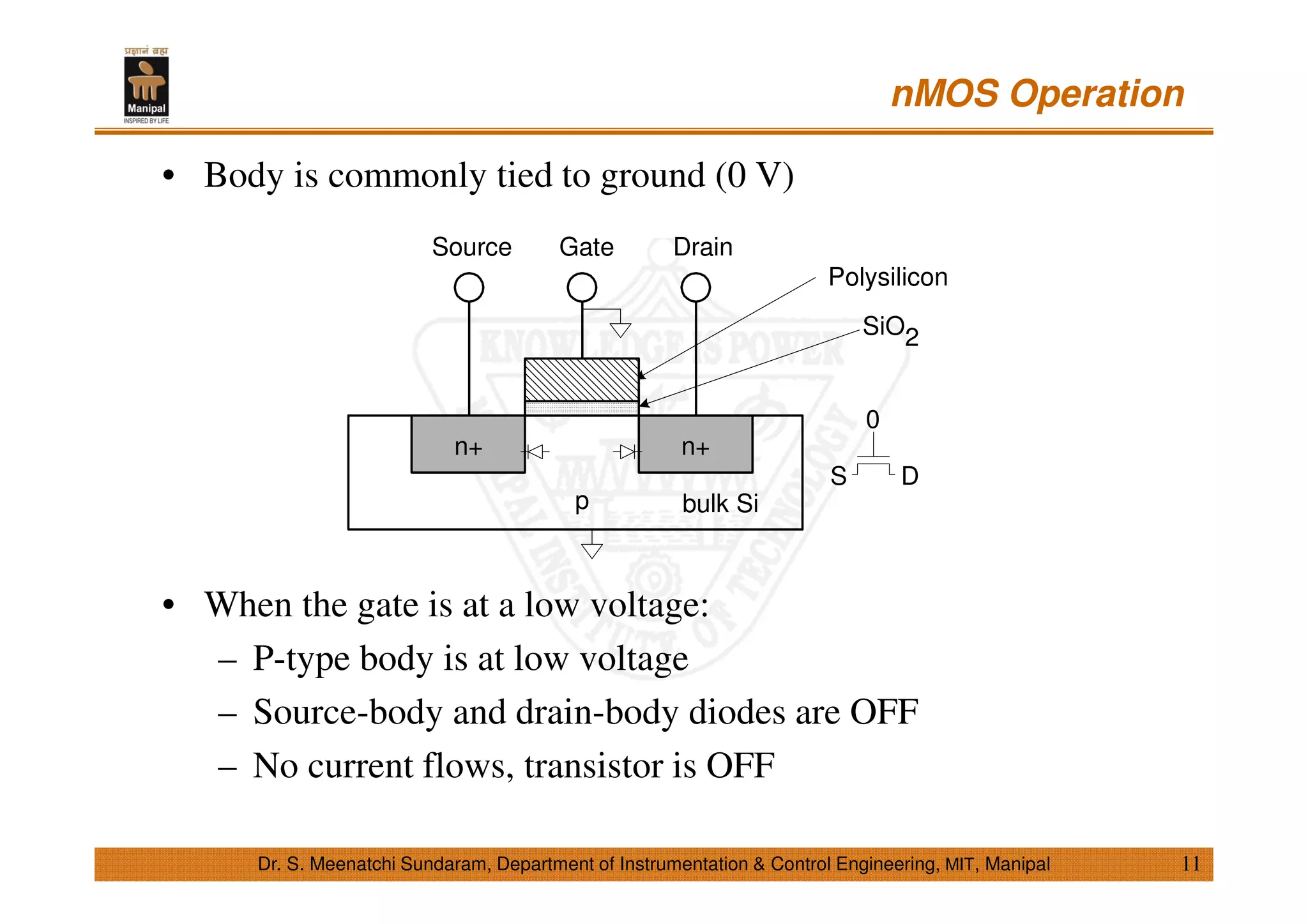
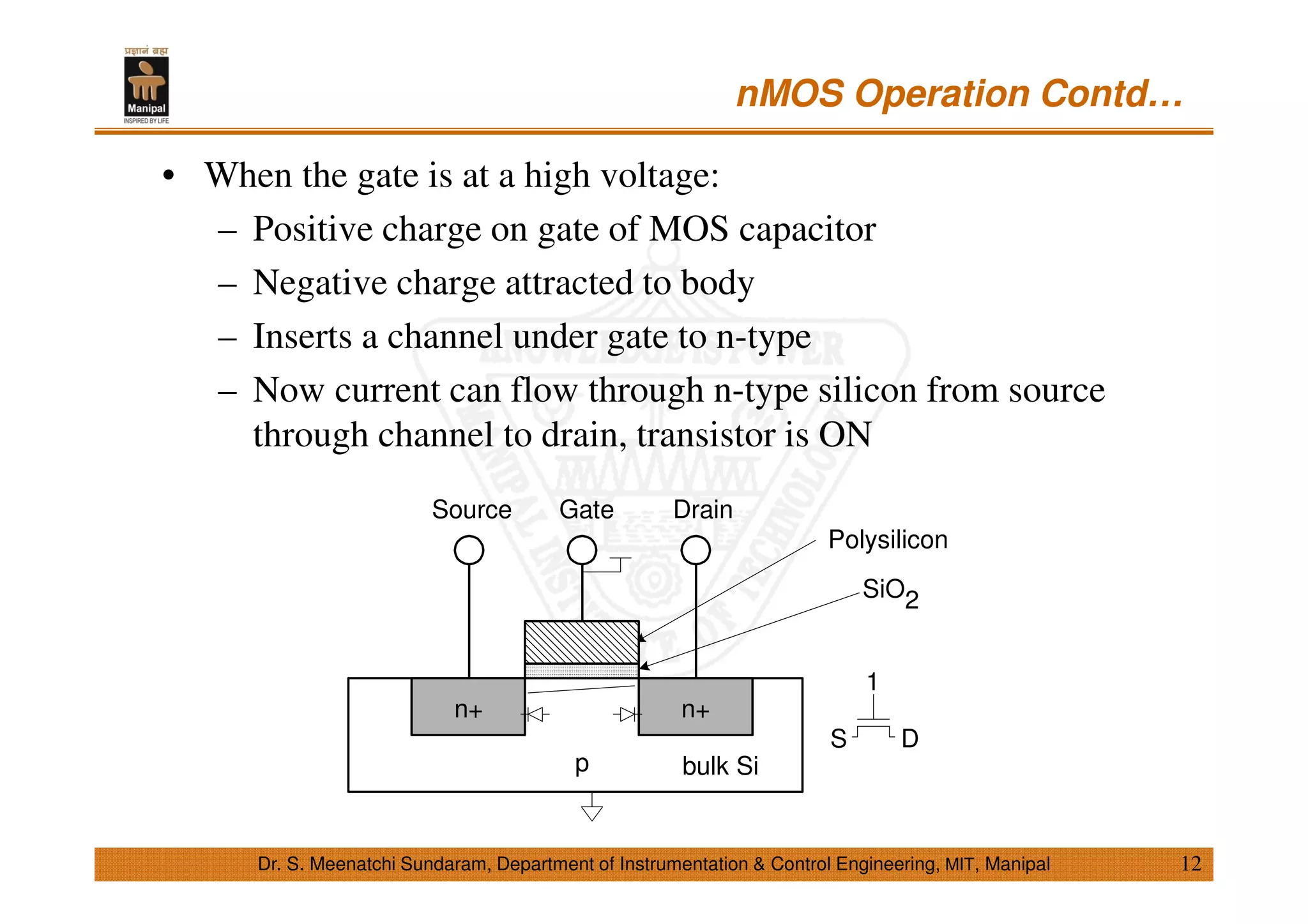
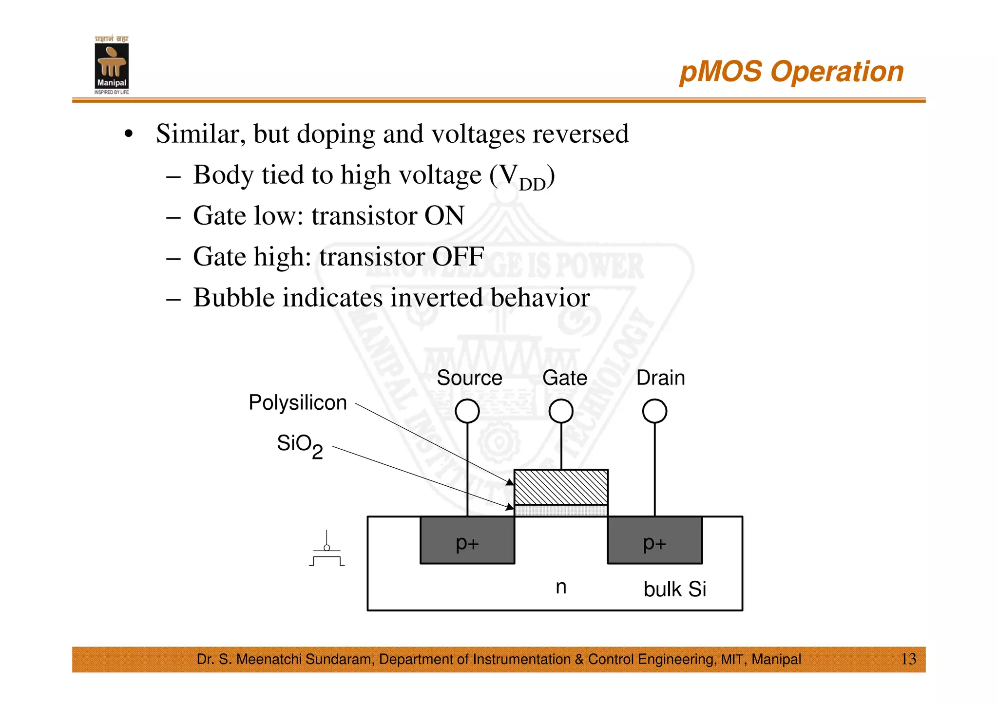

- Wafer production requires tight specifications for diameter, thickness, and flatness of less than 1 micrometer. Over 100 million silicon wafers are produced annually. - Wafers are sliced from silicon crystals and oriented based on Miller indices like (100) or (111) for electronic properties. Flats on wafers indicate doping type and orientation. - CMOS uses complementary pairs of nMOS and pMOS transistors for logic functions. Only one transistor is on at a time, reducing power consumption compared to other technologies like TTL.