Download to read offline


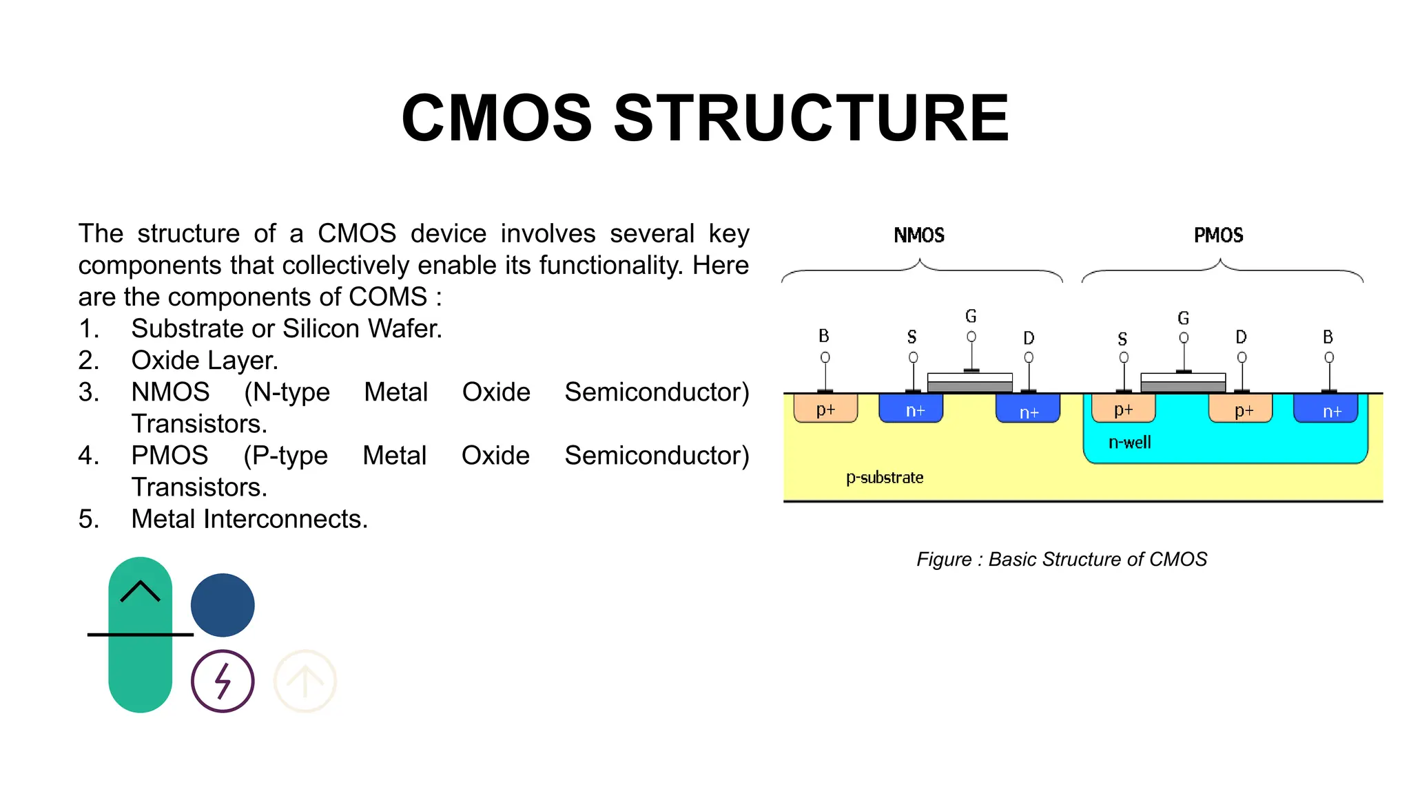


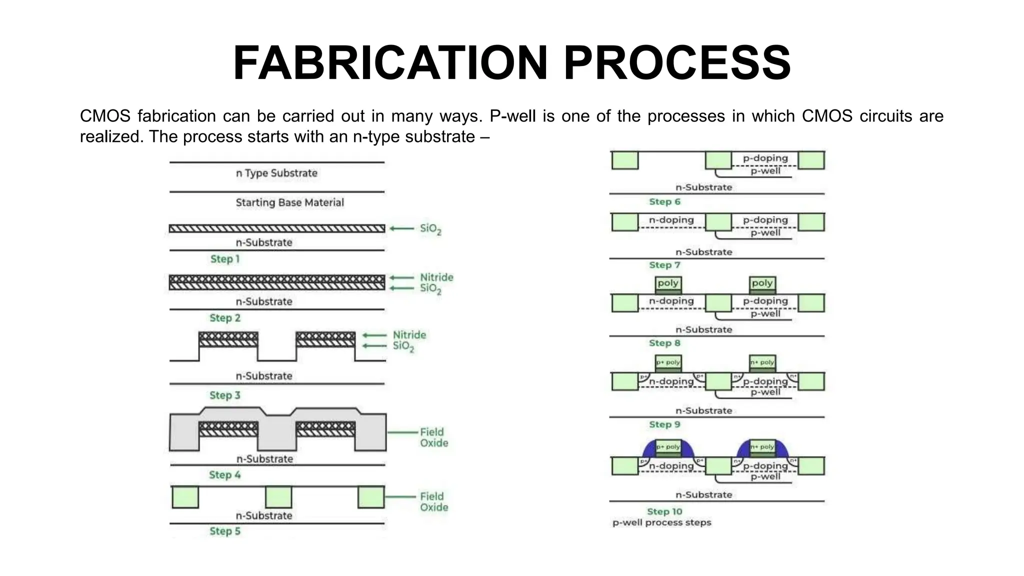


The document presents an overview of CMOS (complementary metal-oxide-semiconductor) technology, detailing its history, structure, and operation of nMOS and pMOS transistors. It covers the CMOS fabrication process and highlights various applications in fields like digital circuits, memory devices, and automotive electronics. The conclusion emphasizes the significance of CMOS technology in modern electronics for its low power consumption and high noise immunity.


