Download as PDF, PPTX
![Silicon Piezoresistors
Piezoresistance = a change in electrical
resistance of solids when
subjected to stress fields. Doped silicon are
piezoresistors (p-type or n-type).
Relationship between change of resistance {ΔR}
and stresses {σ}:
{ΔR} = [π] {σ}
where {ΔR} = { ΔRxx ΔRyy ΔRzz ΔRxy ΔRxz
ΔRyz}T represents the change of resistances in](https://image.slidesharecdn.com/memes2-130621091803-phpapp01/85/The-radio-frequency-microelectromechanical-system-RF-MEMS-Materials-21-320.jpg)
![an infinitesimally small cubic piezoresistive crystal
element with corresponding stress components:
{σ} = {σxx σyy σzz σxy σxz σyz}T and [π] =
piezoresistive coefficient matrix.](https://image.slidesharecdn.com/memes2-130621091803-phpapp01/85/The-radio-frequency-microelectromechanical-system-RF-MEMS-Materials-22-320.jpg)

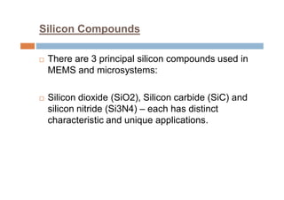
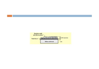
This document discusses the various materials used in silicon-based MEMS and microsystems, highlighting silicon as the primary material, along with its compounds like SiO2, SiC, and Si3N4. It explains the production processes for single-crystal silicon, the properties of piezoresistors, and introduces polymers as emerging materials in the field. Additionally, it compares silicon to other materials like Gallium Arsenide and quartz in terms of their applications and characteristics in MEMS technology.


