1
Analysis and Designof Small Signal
Analysis and Design of Small Signal
Low Frequency BJT Amplifiers
Low Frequency BJT Amplifiers
UNIT – IV
2.
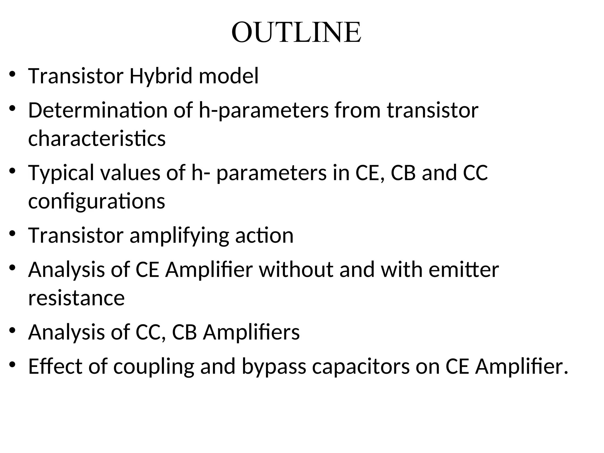
OUTLINE
• Transistor Hybridmodel
• Determination of h-parameters from transistor
characteristics
• Typical values of h- parameters in CE, CB and CC
configurations
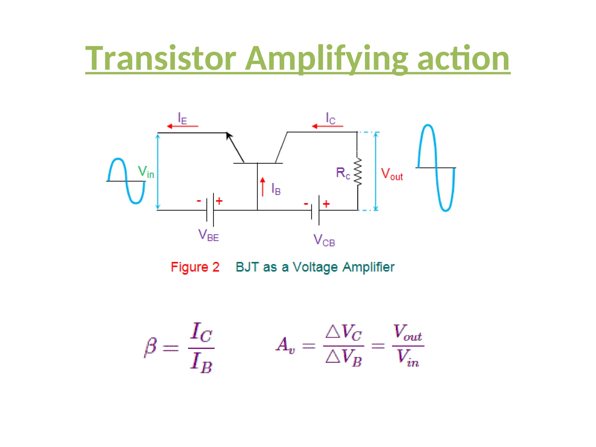
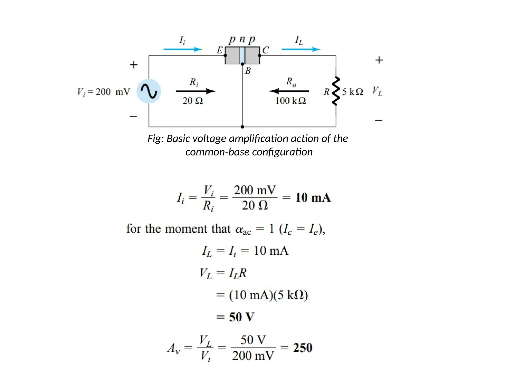
• Transistor amplifying action
• Analysis of CE Amplifier without and with emitter
resistance
• Analysis of CC, CB Amplifiers
• Effect of coupling and bypass capacitors on CE Amplifier.
3.
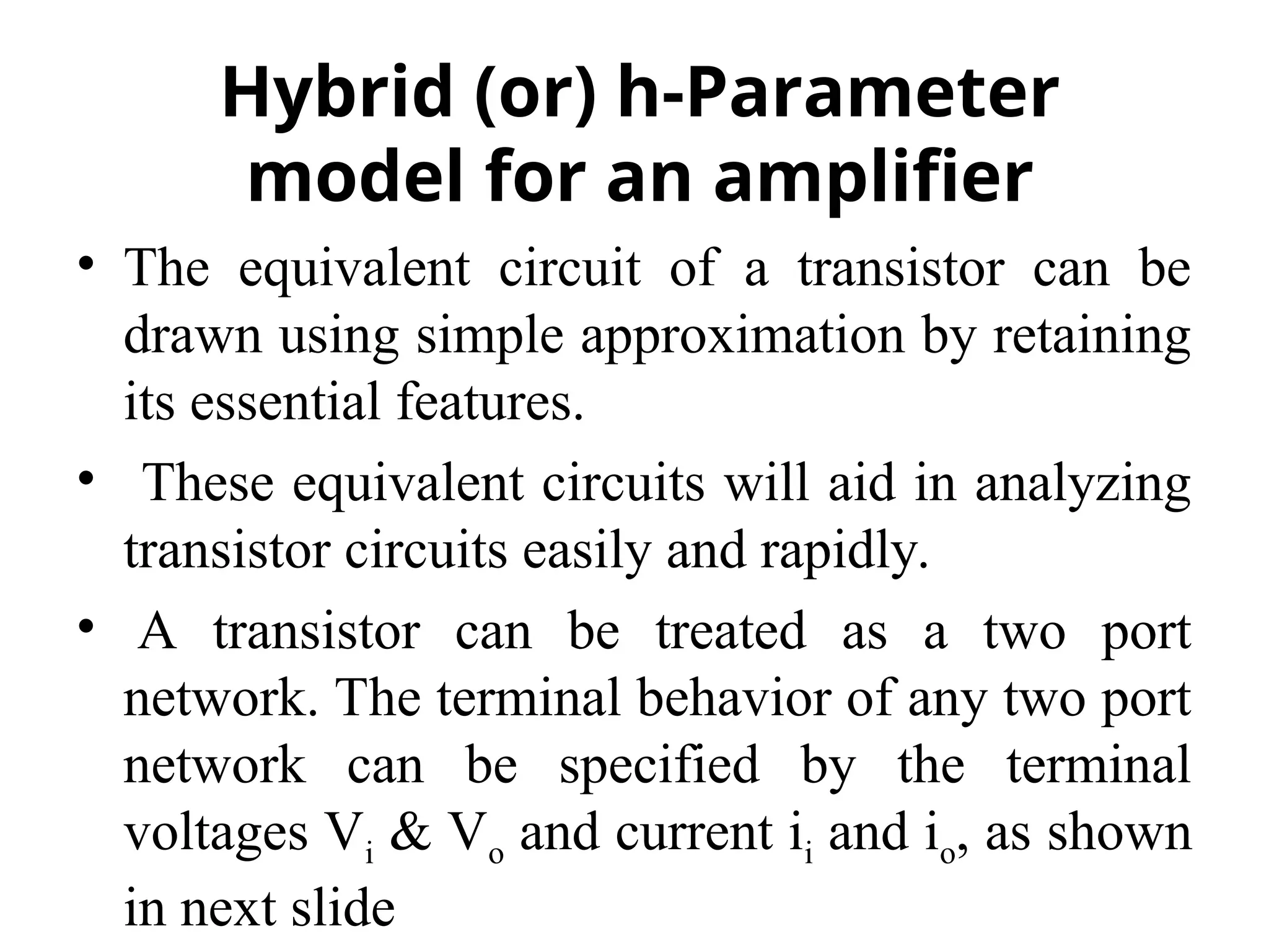
• The equivalentcircuit of a transistor can be
drawn using simple approximation by retaining
its essential features.
• These equivalent circuits will aid in analyzing
transistor circuits easily and rapidly.
• A transistor can be treated as a two port
network. The terminal behavior of any two port
network can be specified by the terminal
voltages Vi & Vo and current ii and io, as shown
in next slide
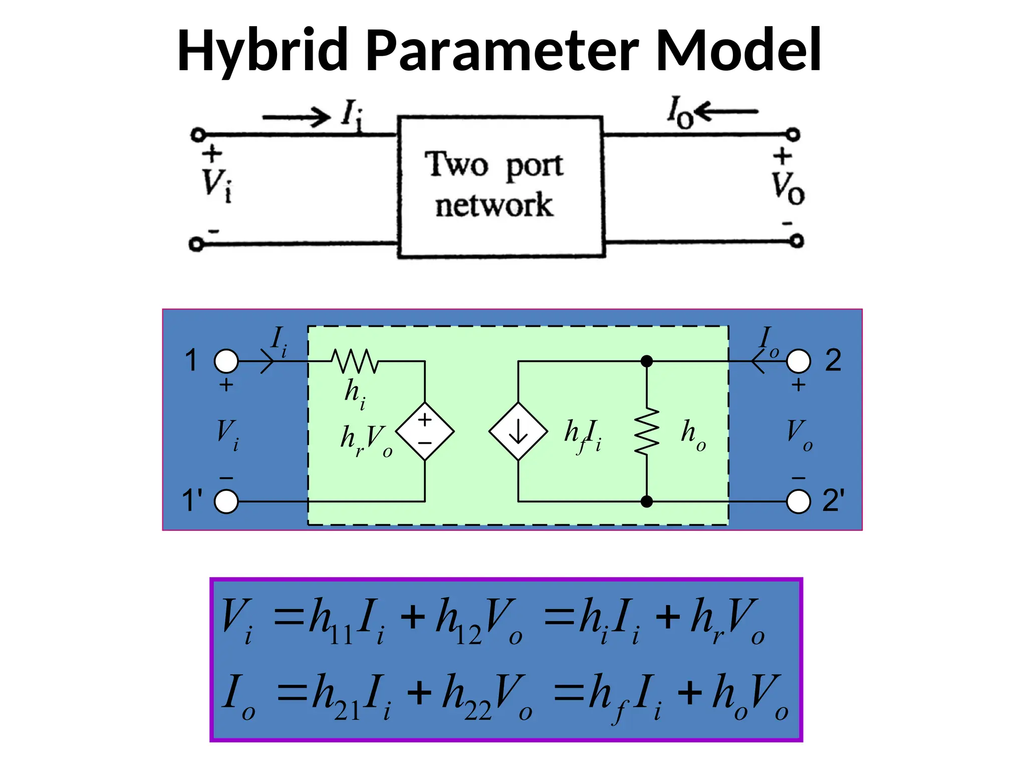
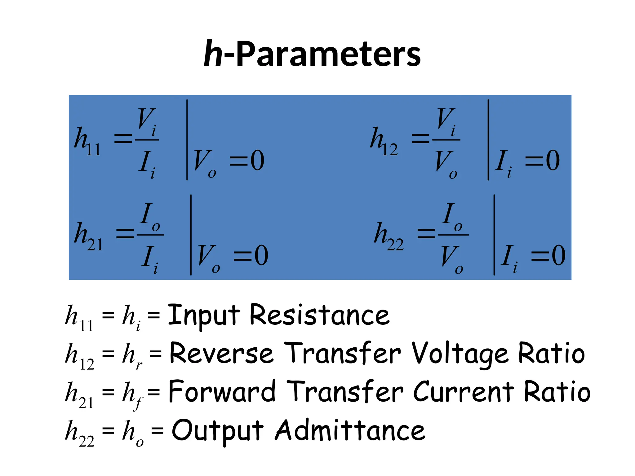
Hybrid (or) h-Parameter
model for an amplifier
11 12
21 22
00
0 0
i i
o i
i o
o o
o i
i o
V V
h h
V I
I V
I I
h h
V I
I V
h-Parameters
h11 = hi = Input Resistance
h12 = hr = Reverse Transfer Voltage Ratio
h21 = hf = Forward Transfer Current Ratio
h22 = ho = Output Admittance
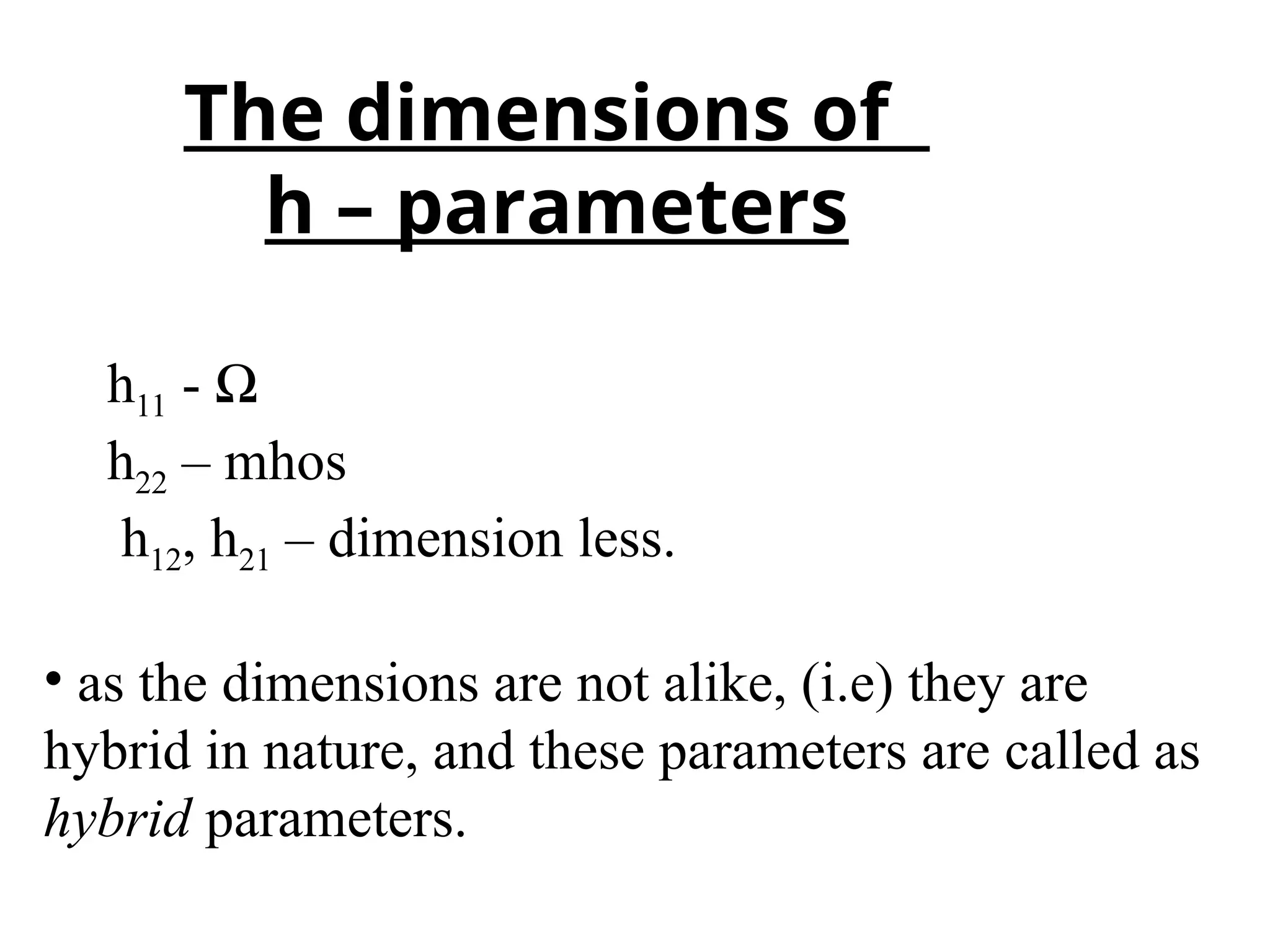
6.
h11 - Ω
h22– mhos
h12, h21 – dimension less.
• as the dimensions are not alike, (i.e) they are
hybrid in nature, and these parameters are called as
hybrid parameters.
The dimensions of
h – parameters
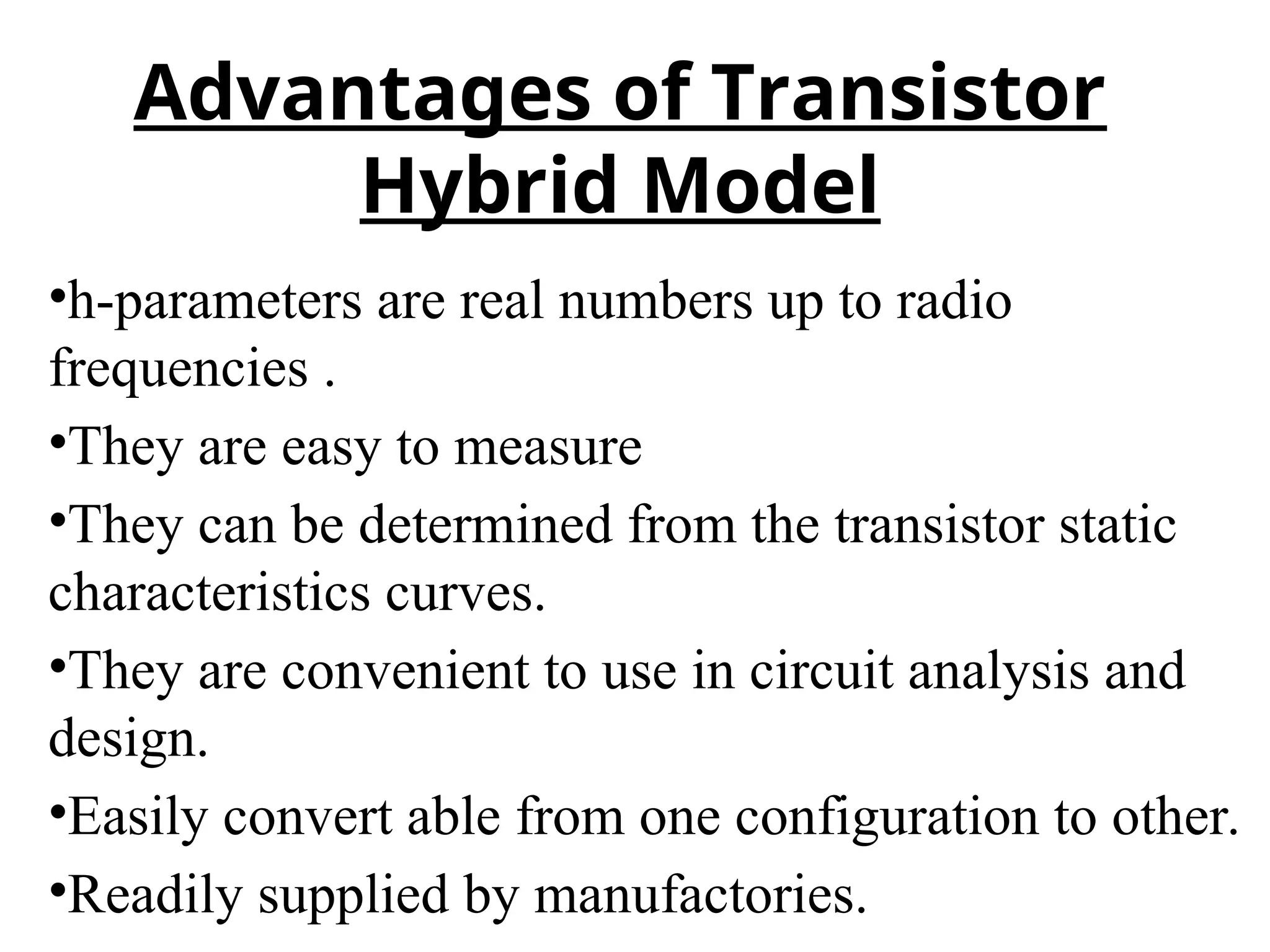
7.
•h-parameters are realnumbers up to radio
frequencies .
•They are easy to measure
•They can be determined from the transistor static
characteristics curves.
•They are convenient to use in circuit analysis and
design.
•Easily convert able from one configuration to other.
•Readily supplied by manufactories.
Advantages of Transistor
Hybrid Model
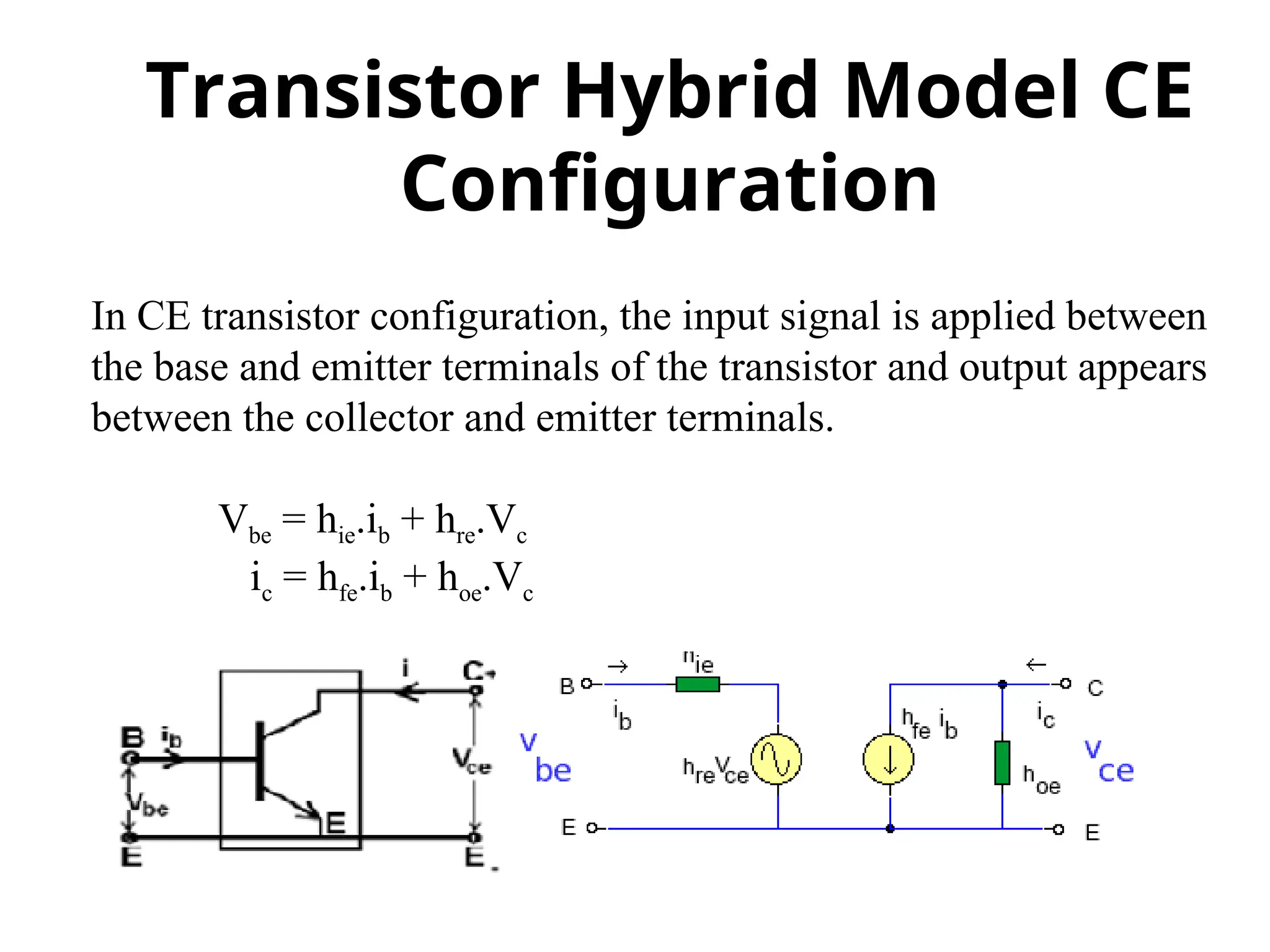
8.
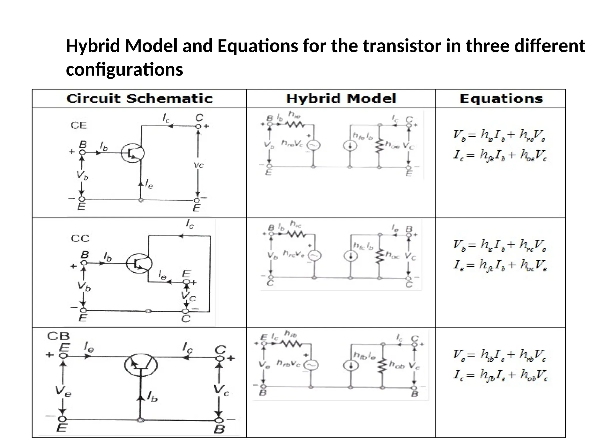
In CE transistorconfiguration, the input signal is applied between
the base and emitter terminals of the transistor and output appears
between the collector and emitter terminals.
Vbe = hie.ib + hre.Vc
ic = hfe.ib + hoe.Vc
Transistor Hybrid Model CE
Configuration
9.
Hybrid Model andEquations for the transistor in three different
configurations
10.
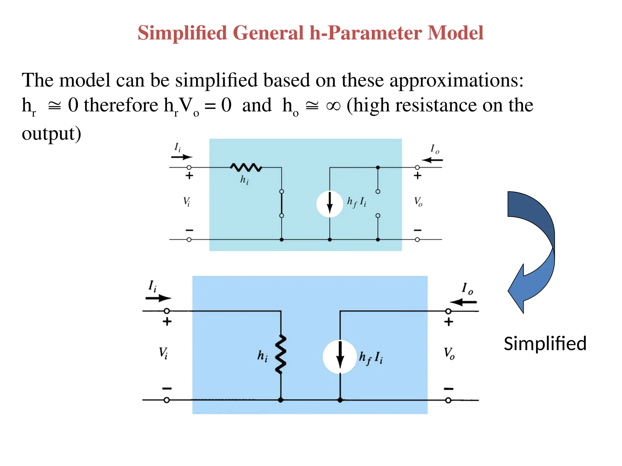
Simplified General h-ParameterModel
The model can be simplified based on these approximations:
hr 0 therefore hrVo = 0 and ho (high resistance on the
output)
Simplified
11.
Determination of h-parametersfrom
characteristics
Input
Characteristics: To
obtain input resistance
find VBE
and IB
for a
constant VCE
on one of
the input characteristics.
Input impedance = hie
= Ri
= VBE
/ IB
(VCE
is constant)
Reverse voltage gain = hre
= VEB
/ VCE
(IB
= constant)
12.
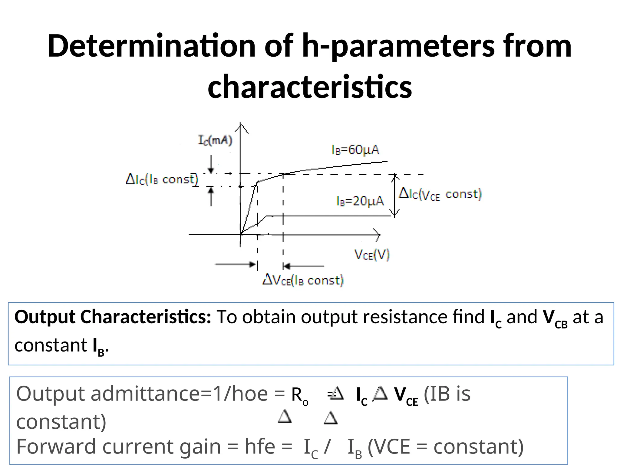
Determination of h-parametersfrom
characteristics
Output Characteristics: To obtain output resistance find IC and VCB at a
constant IB.
Output admittance=1/hoe = Ro = IC / VCE (IB is
constant)
Forward current gain = hfe = IC / IB (VCE = constant)
13.
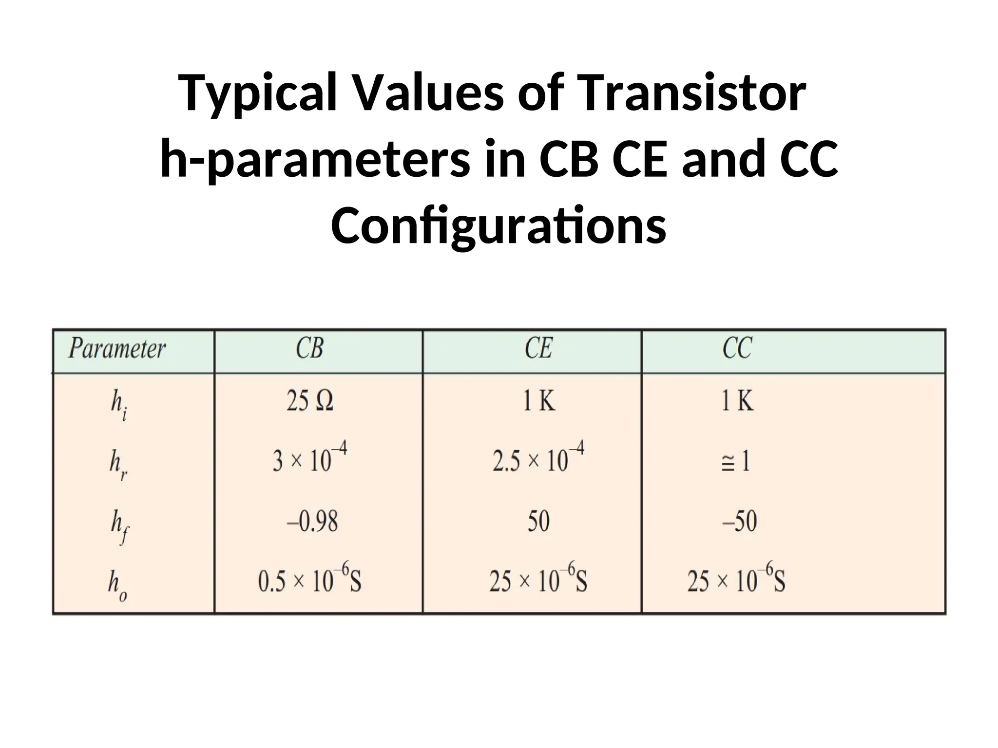
Typical Values ofTransistor
h-parameters in CB CE and CC
Configurations
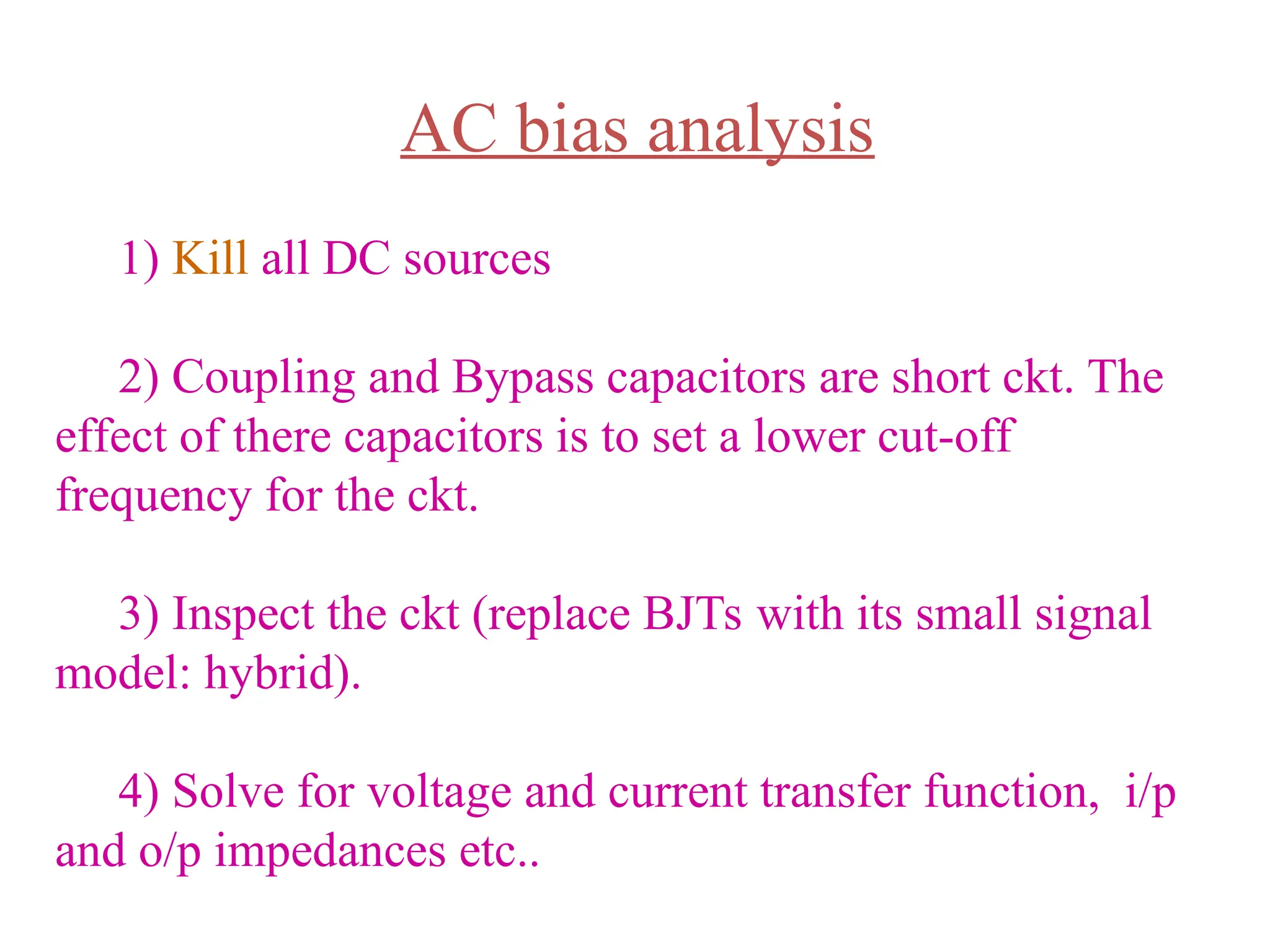
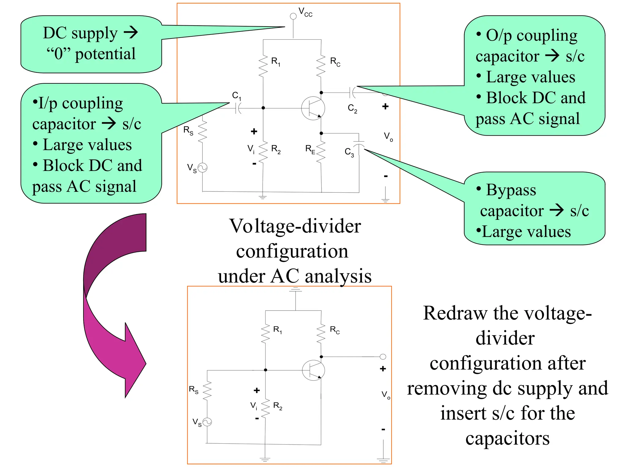
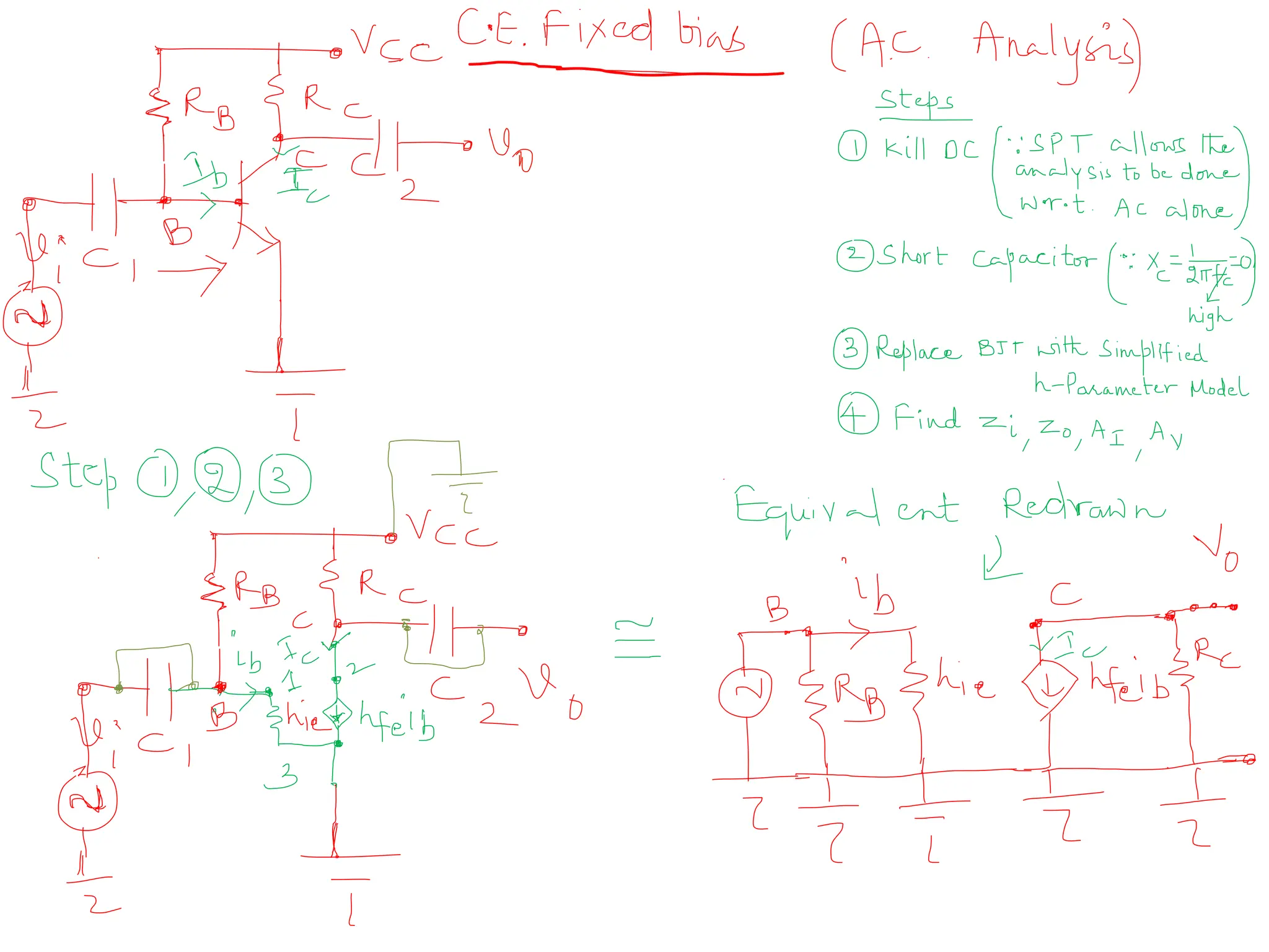
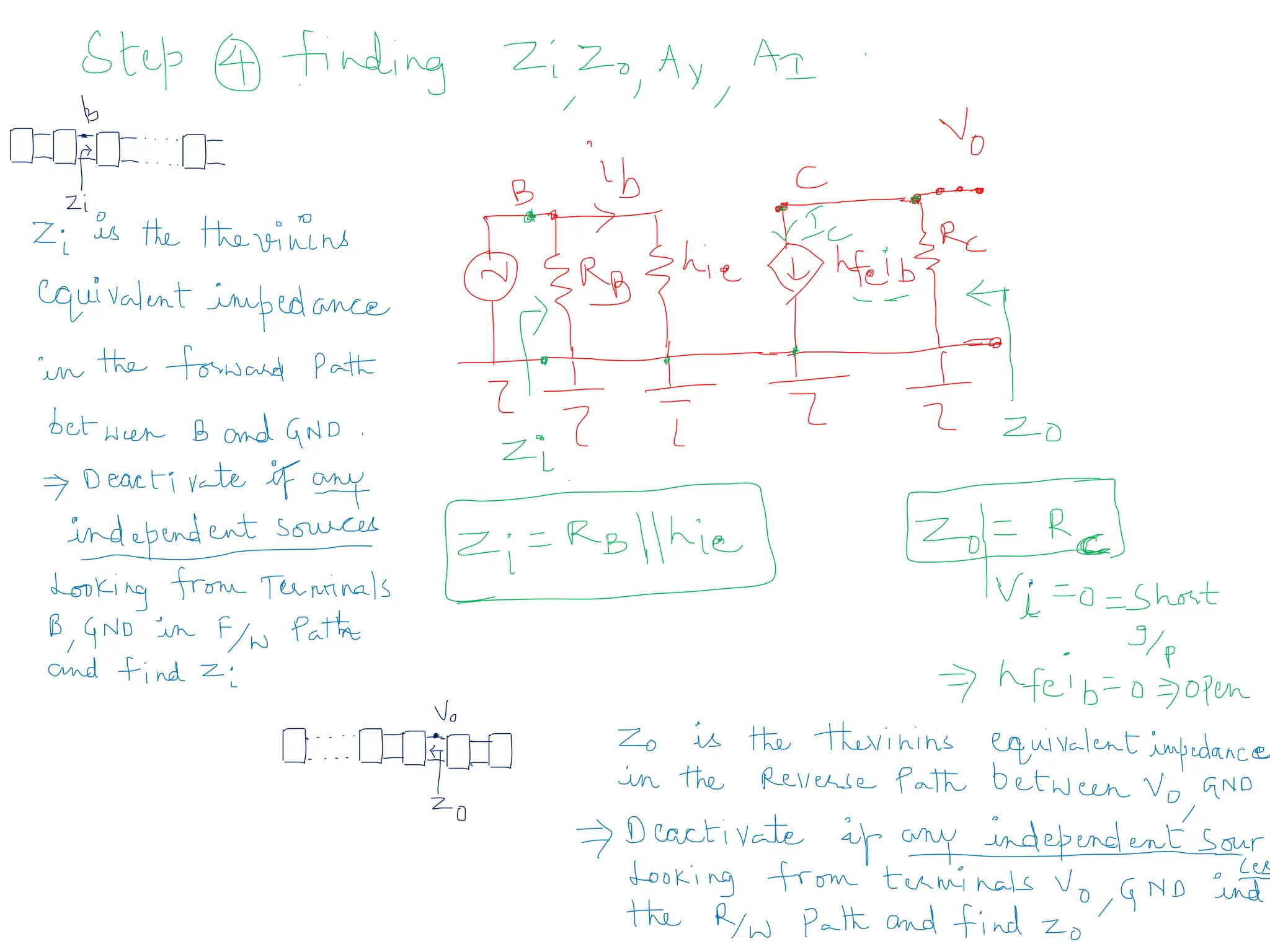
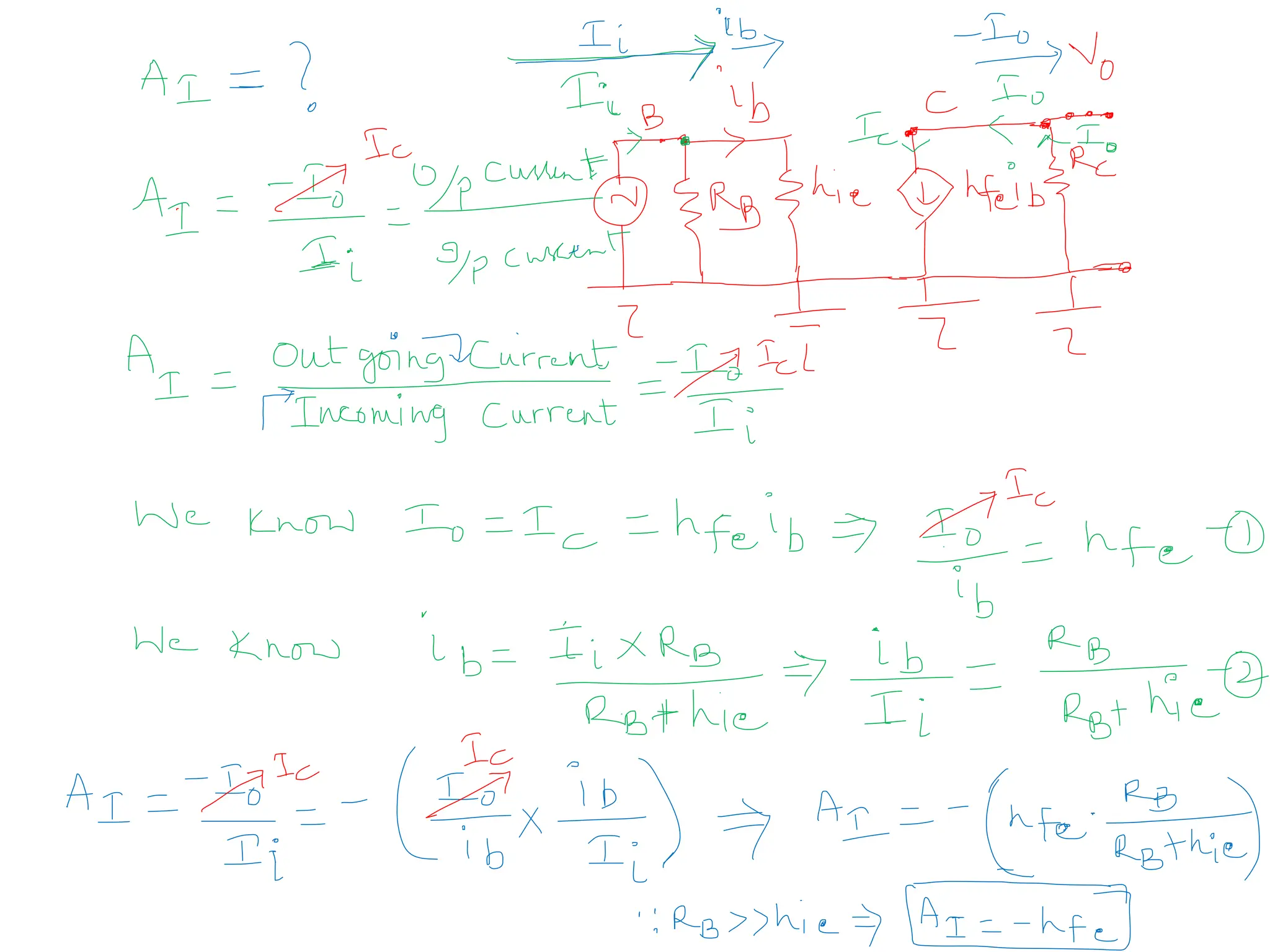
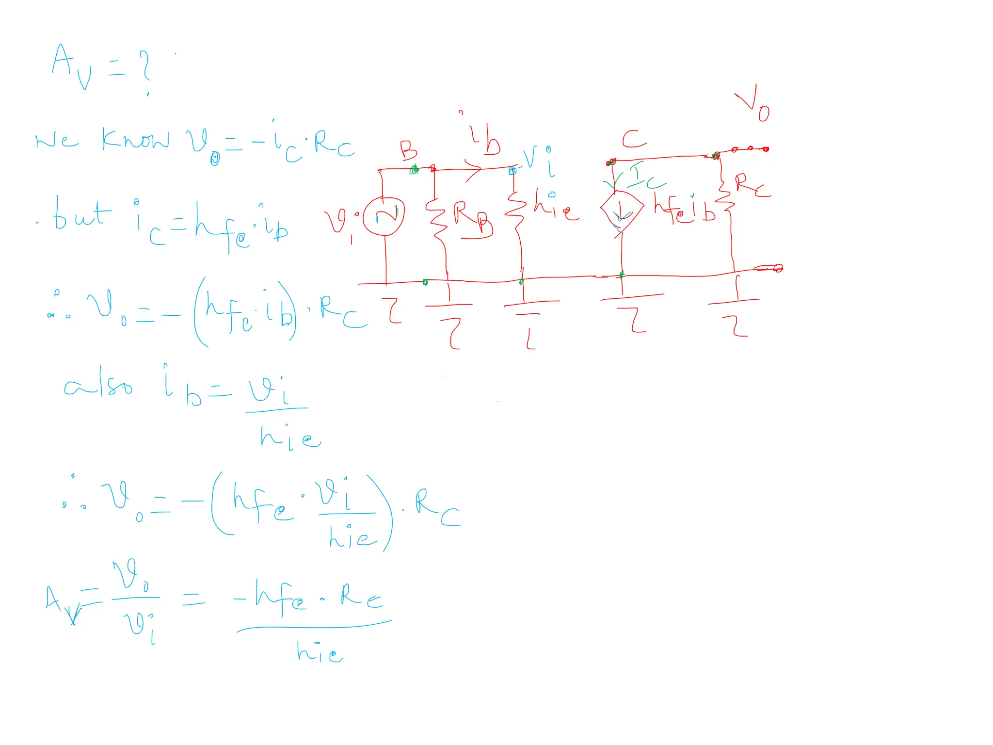
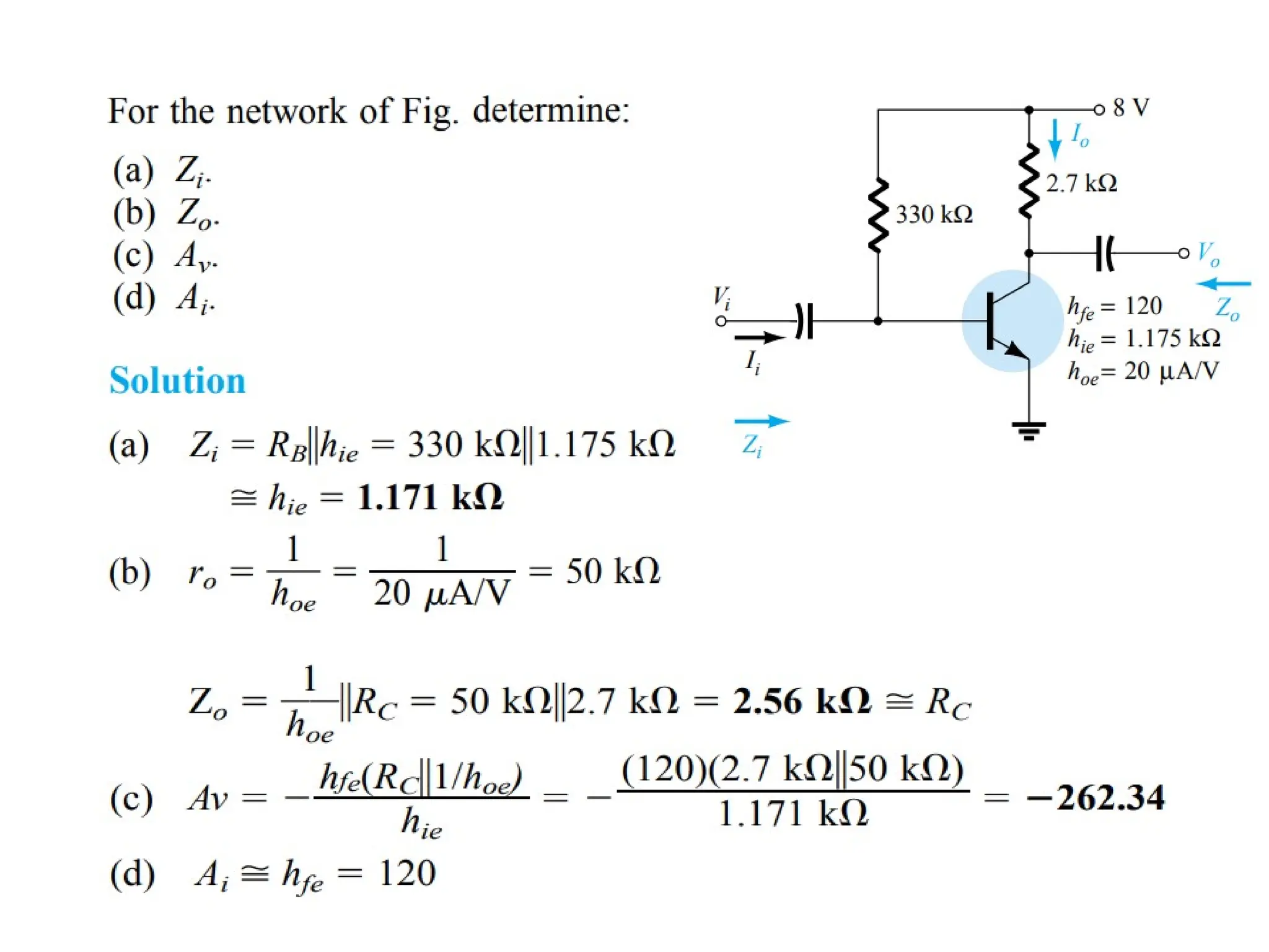
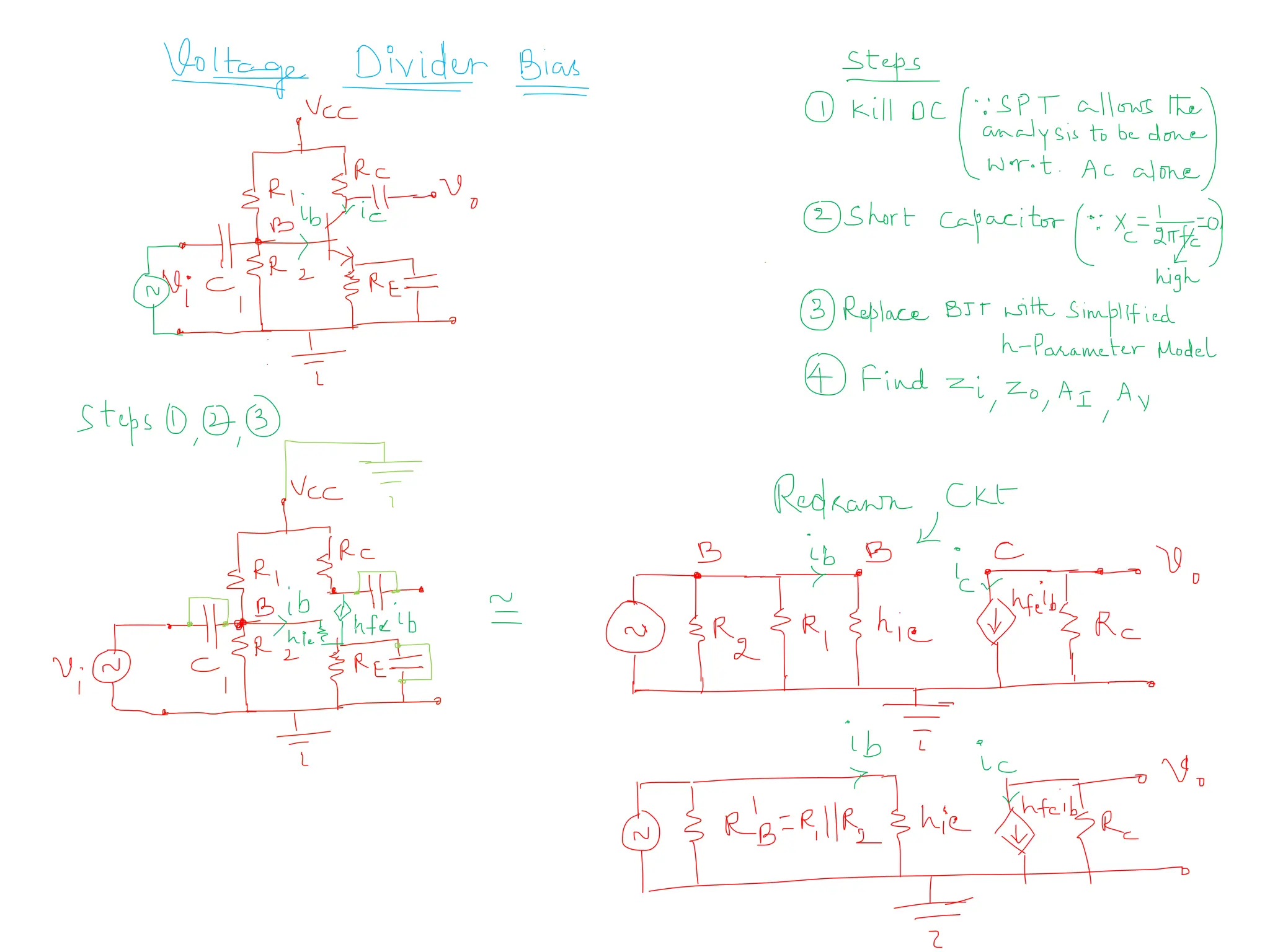
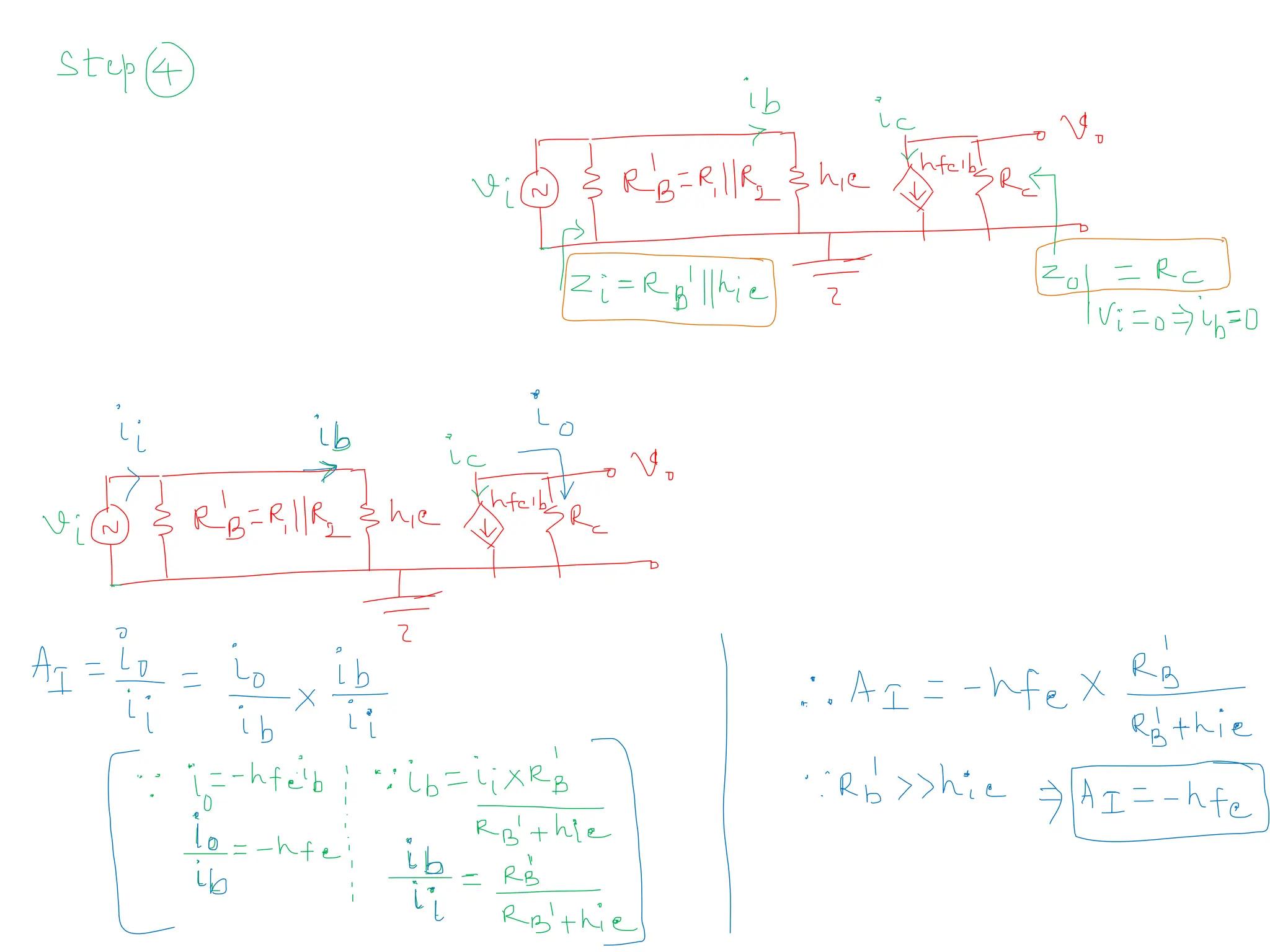
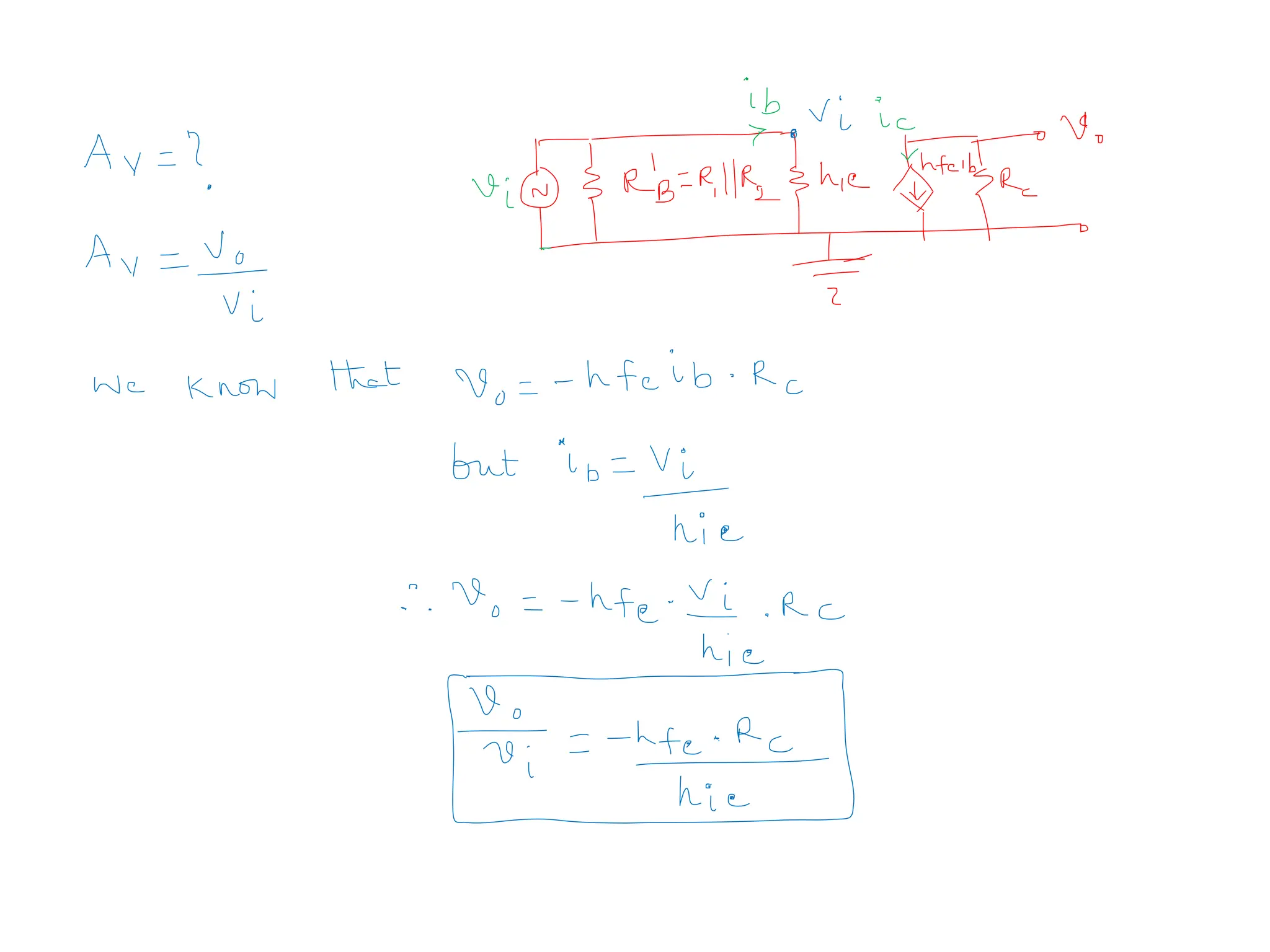
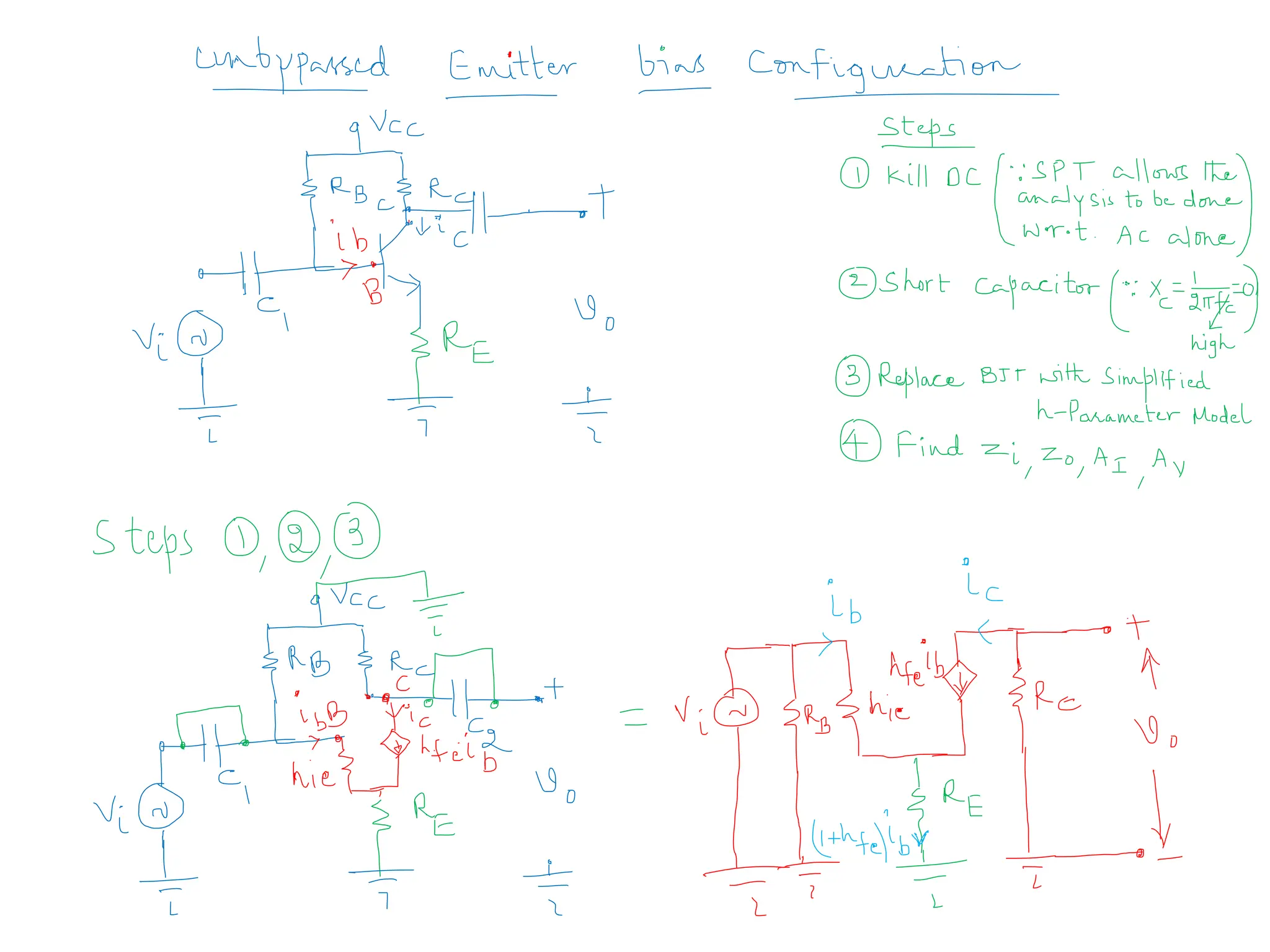
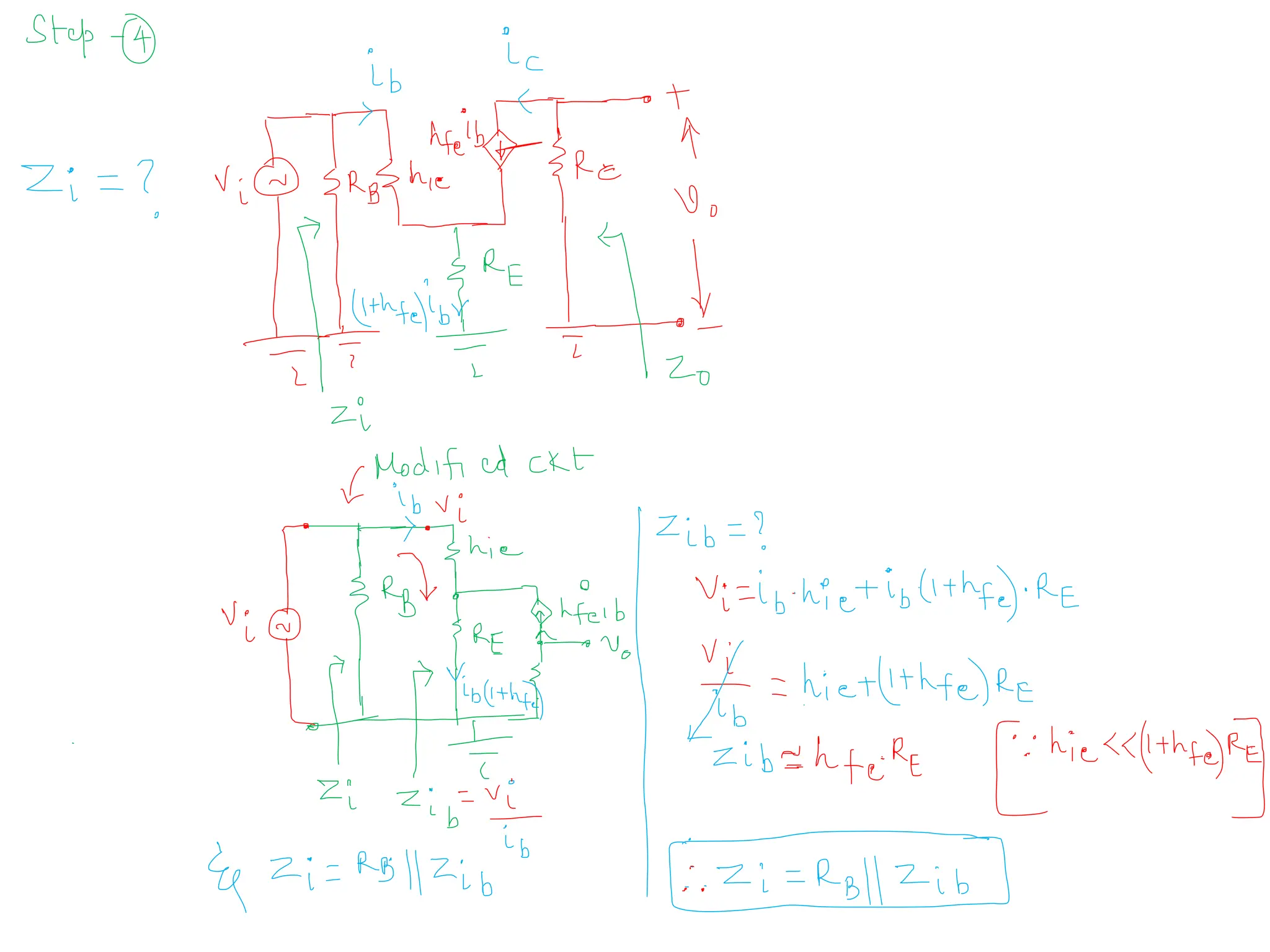
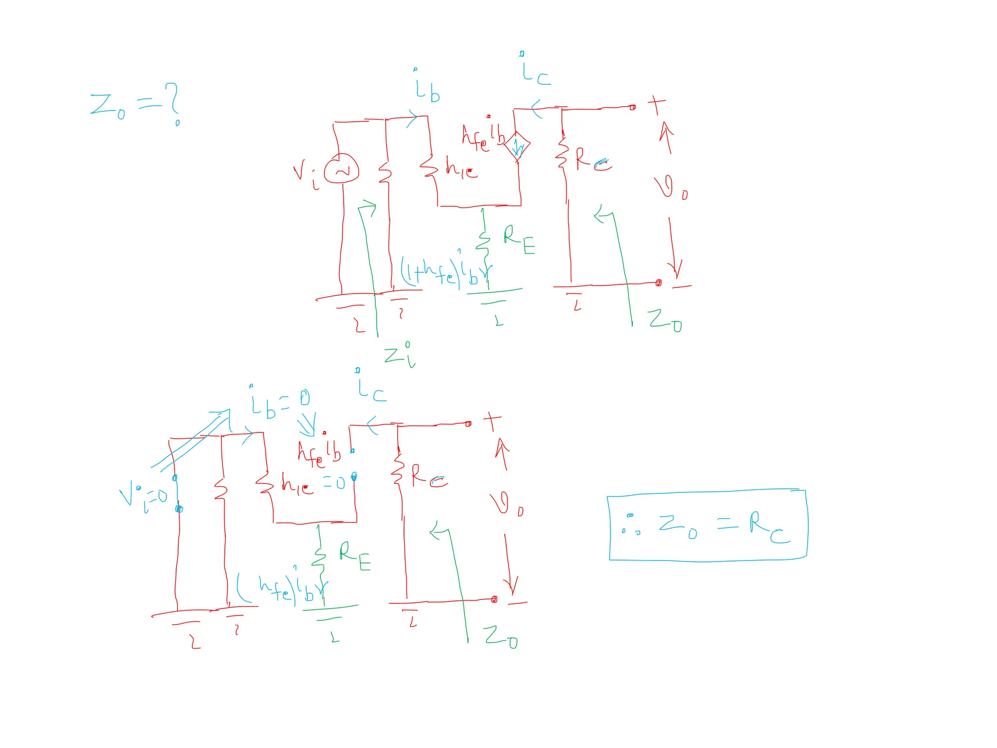
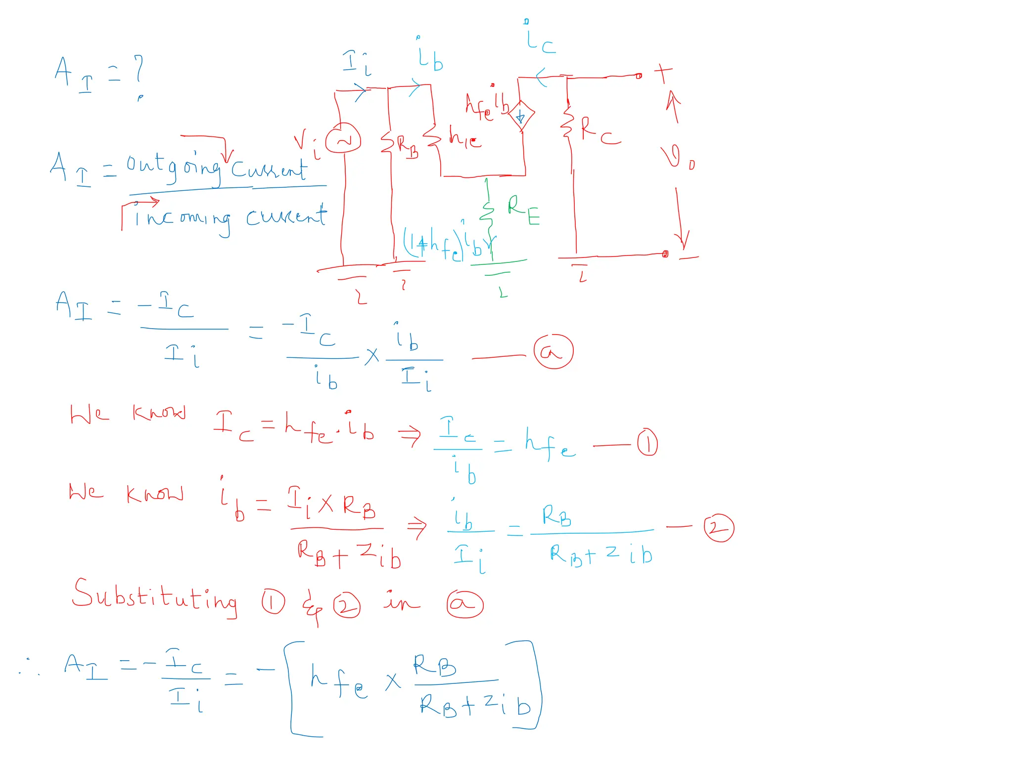
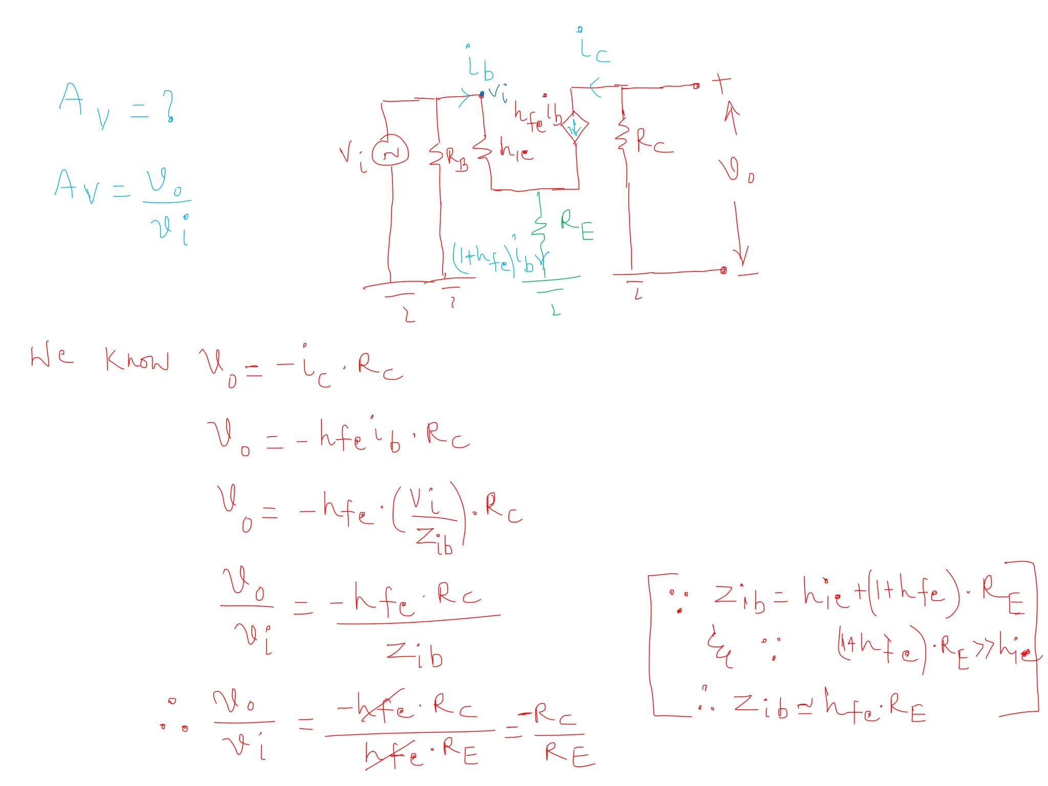
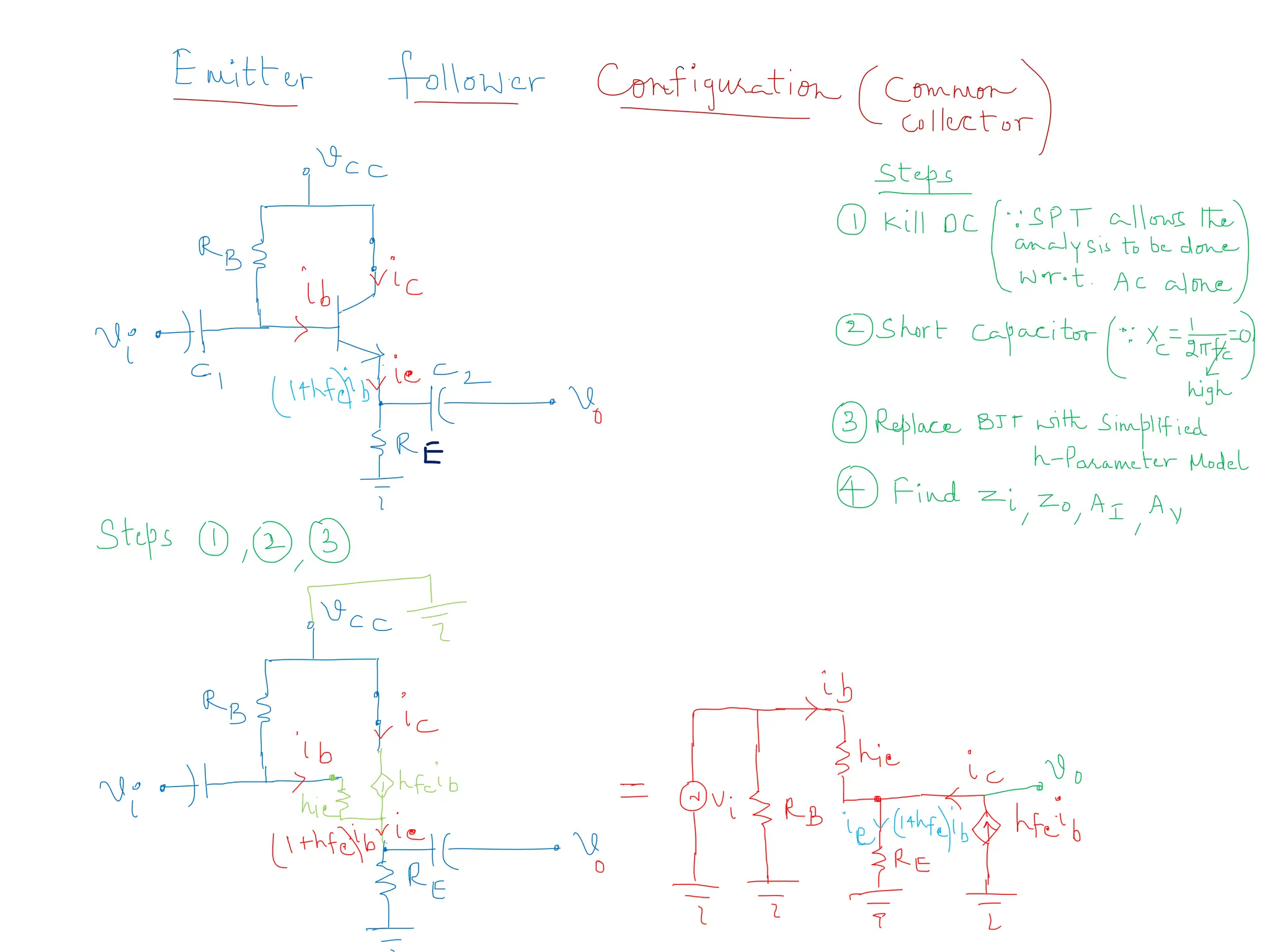
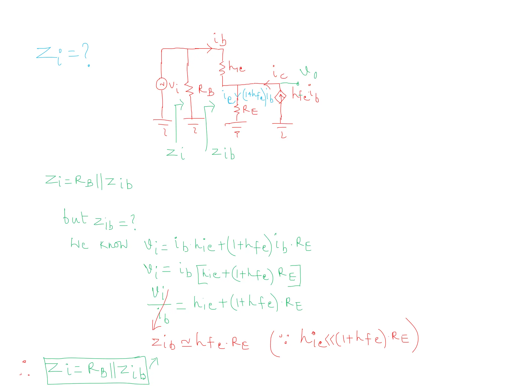
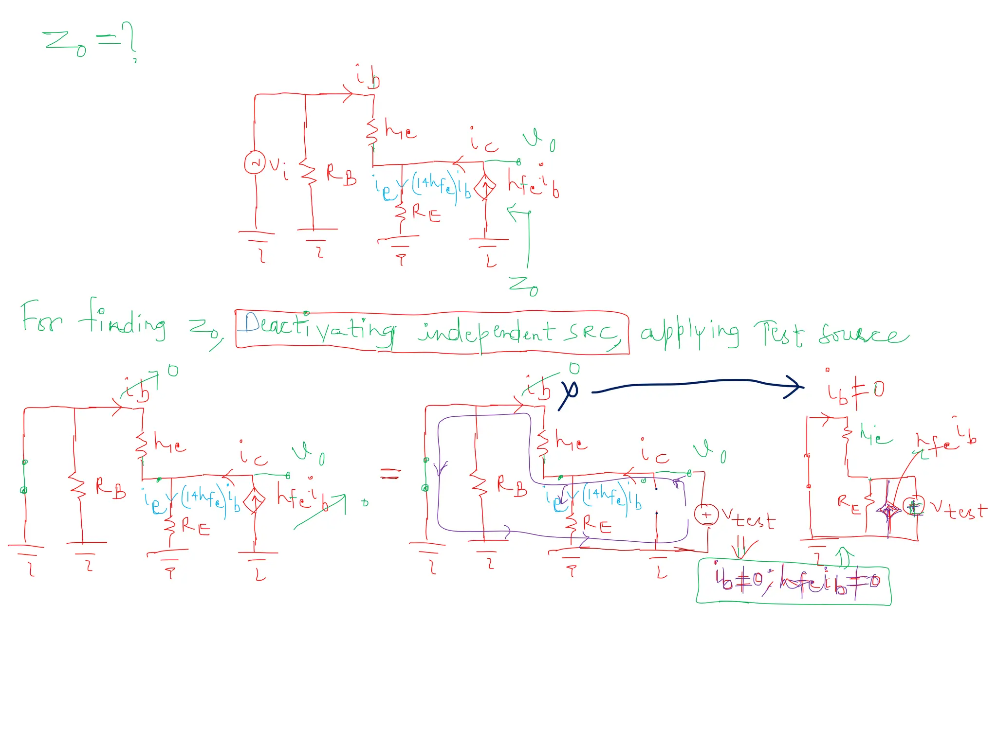
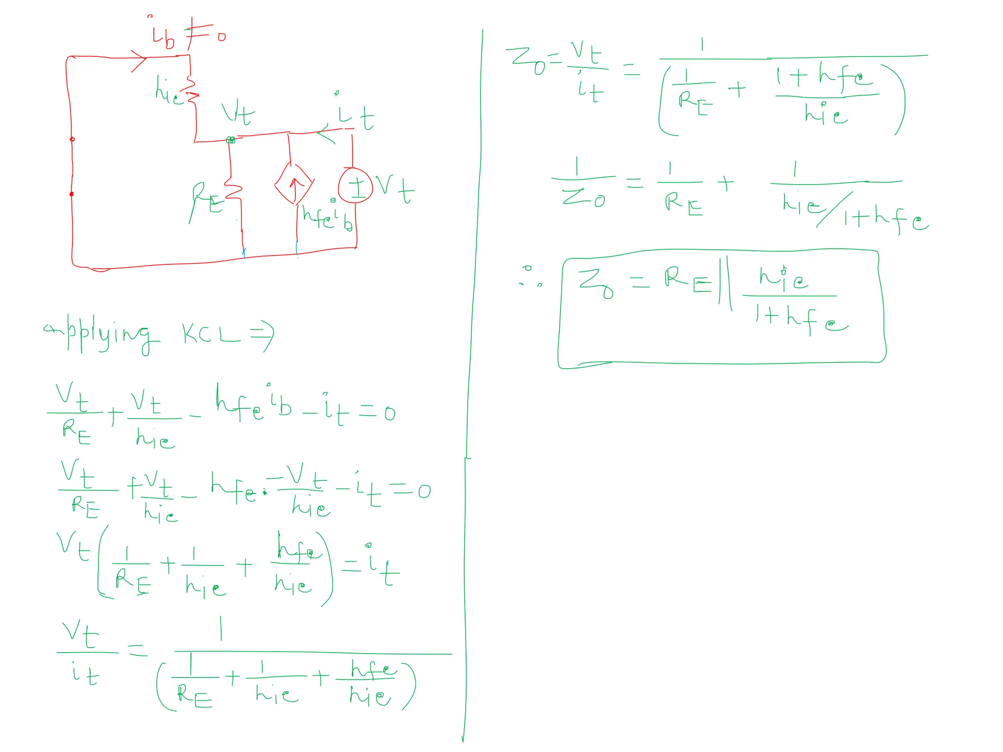
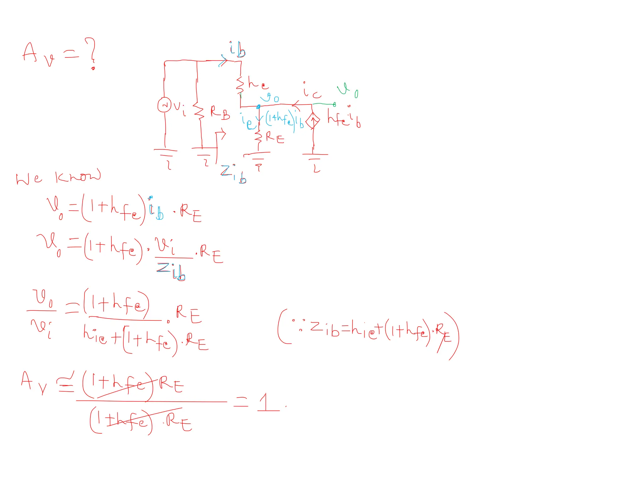
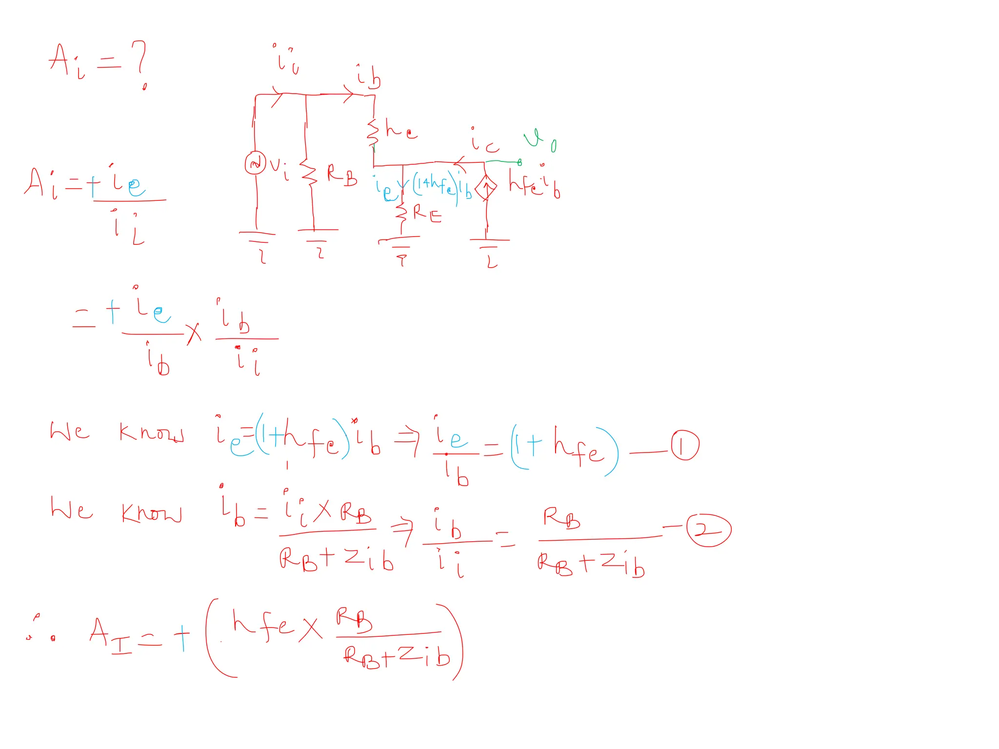
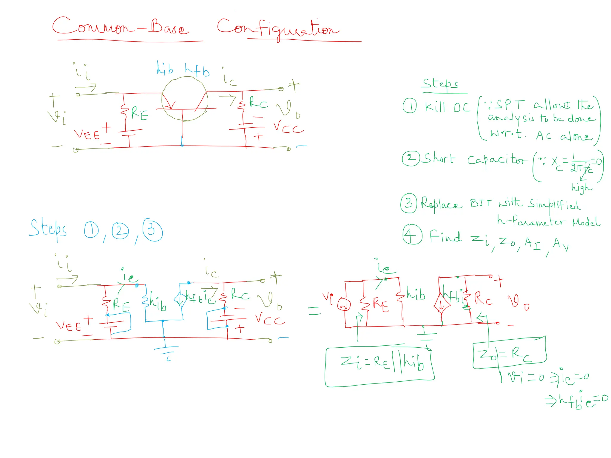
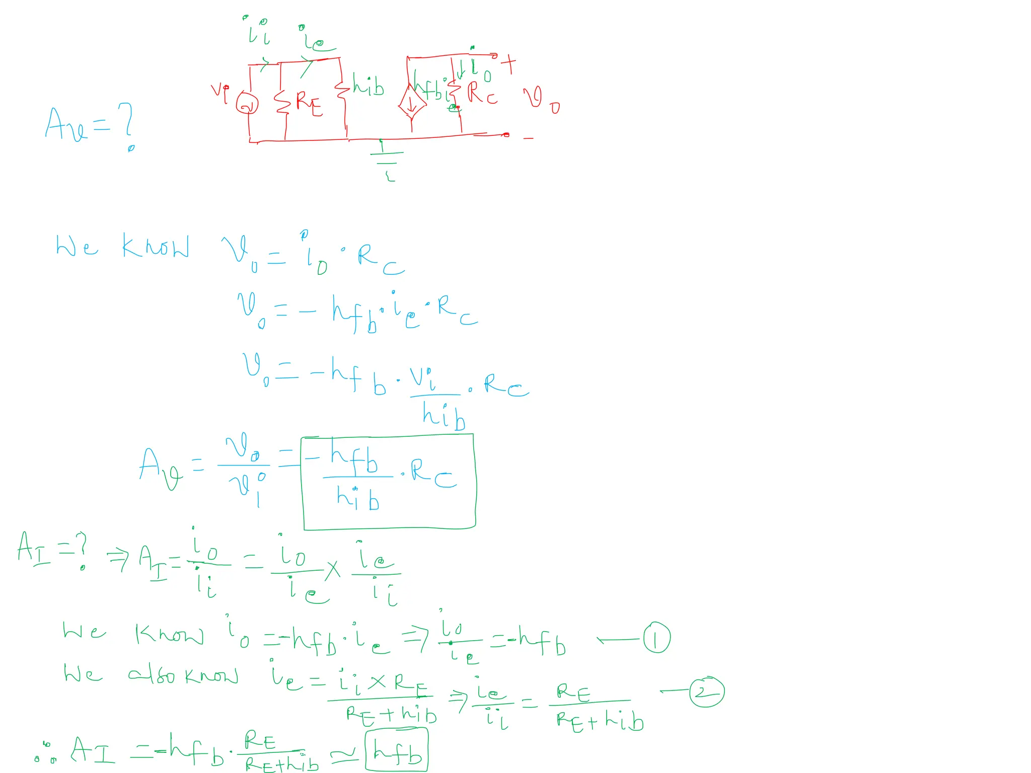
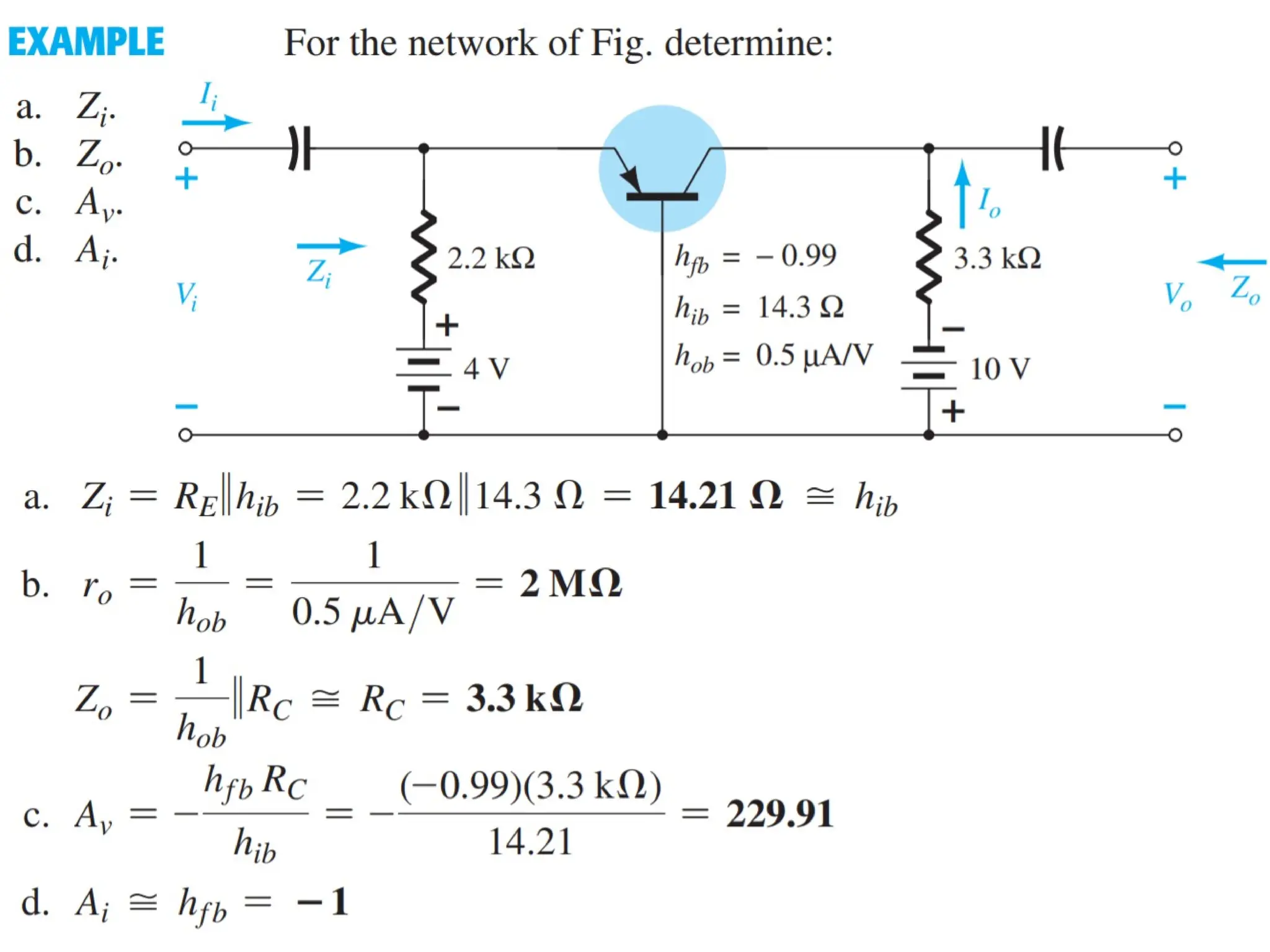
AC bias analysis
1)Kill all DC sources
2) Coupling and Bypass capacitors are short ckt. The
effect of there capacitors is to set a lower cut-off
frequency for the ckt.
3) Inspect the ckt (replace BJTs with its small signal
model: hybrid).
4) Solve for voltage and current transfer function, i/p
and o/p impedances etc..
17.
VS
VCC
C1
C2
C3
+
-
Vo
RS
Vi
+
-
RE
RC
R1
R2
VS
+
-
Vo
RS
Vi
+
-
RC
R1
R2
•I/p coupling
capacitor s/c
• Large values
• Block DC and
pass AC signal • Bypass
capacitor s/c
•Large values
DC supply
“0” potential
Voltage-divider
configuration
under AC analysis
Redraw the voltage-
divider
configuration after
removing dc supply and
insert s/c for the
capacitors
• O/p coupling
capacitor s/c
• Large values
• Block DC and
pass AC signal
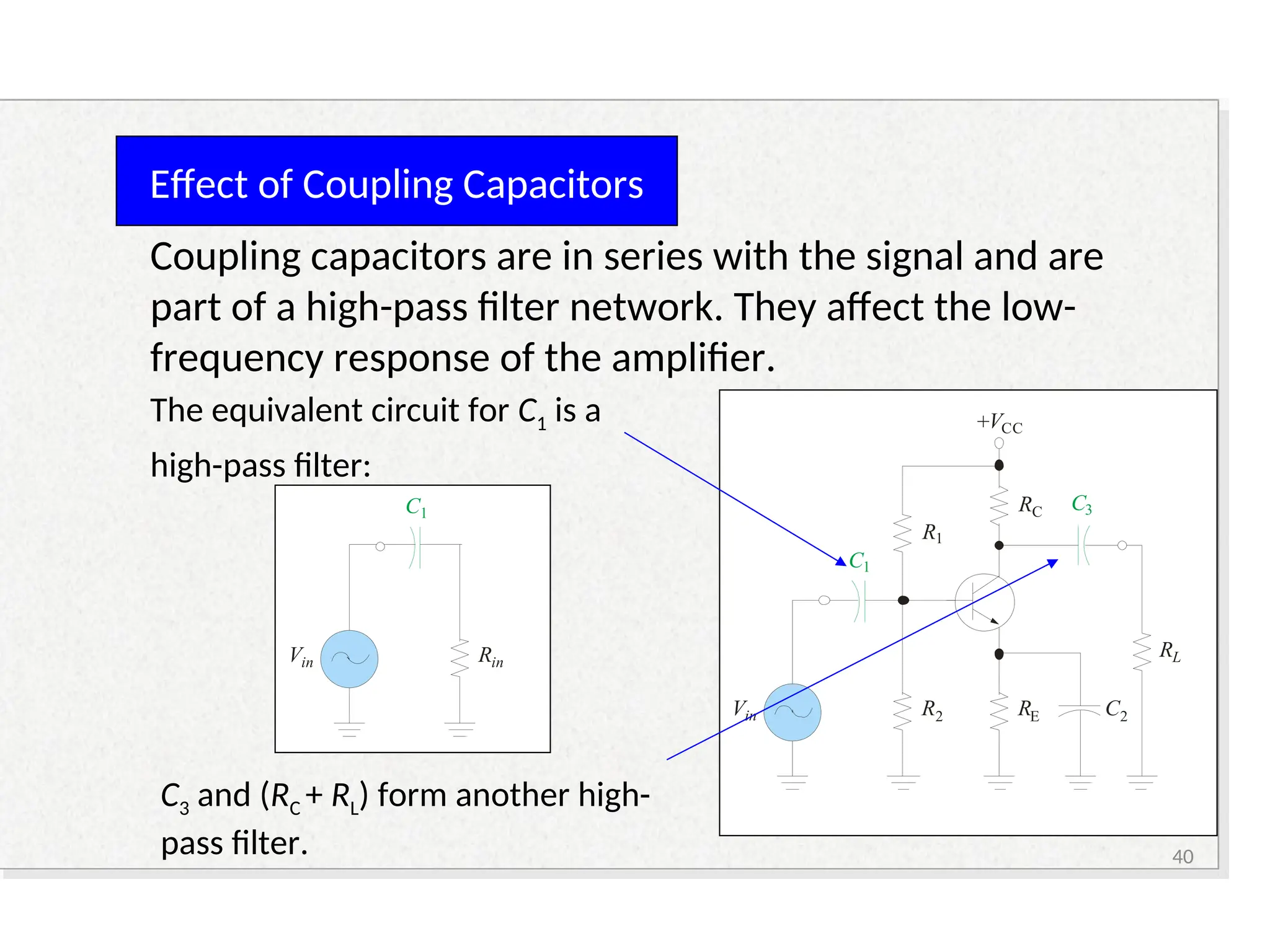
Effect of CouplingCapacitors
Coupling capacitors are in series with the signal and are
part of a high-pass filter network. They affect the low-
frequency response of the amplifier.
RC
+VCC
R2
Vin
R1
RE
RL
C
C
1
3
C2
The equivalent circuit for C1 is a
high-pass filter:
Rin
Vin
C1
C3 and (RC + RL) form another high-
pass filter. 40
41.
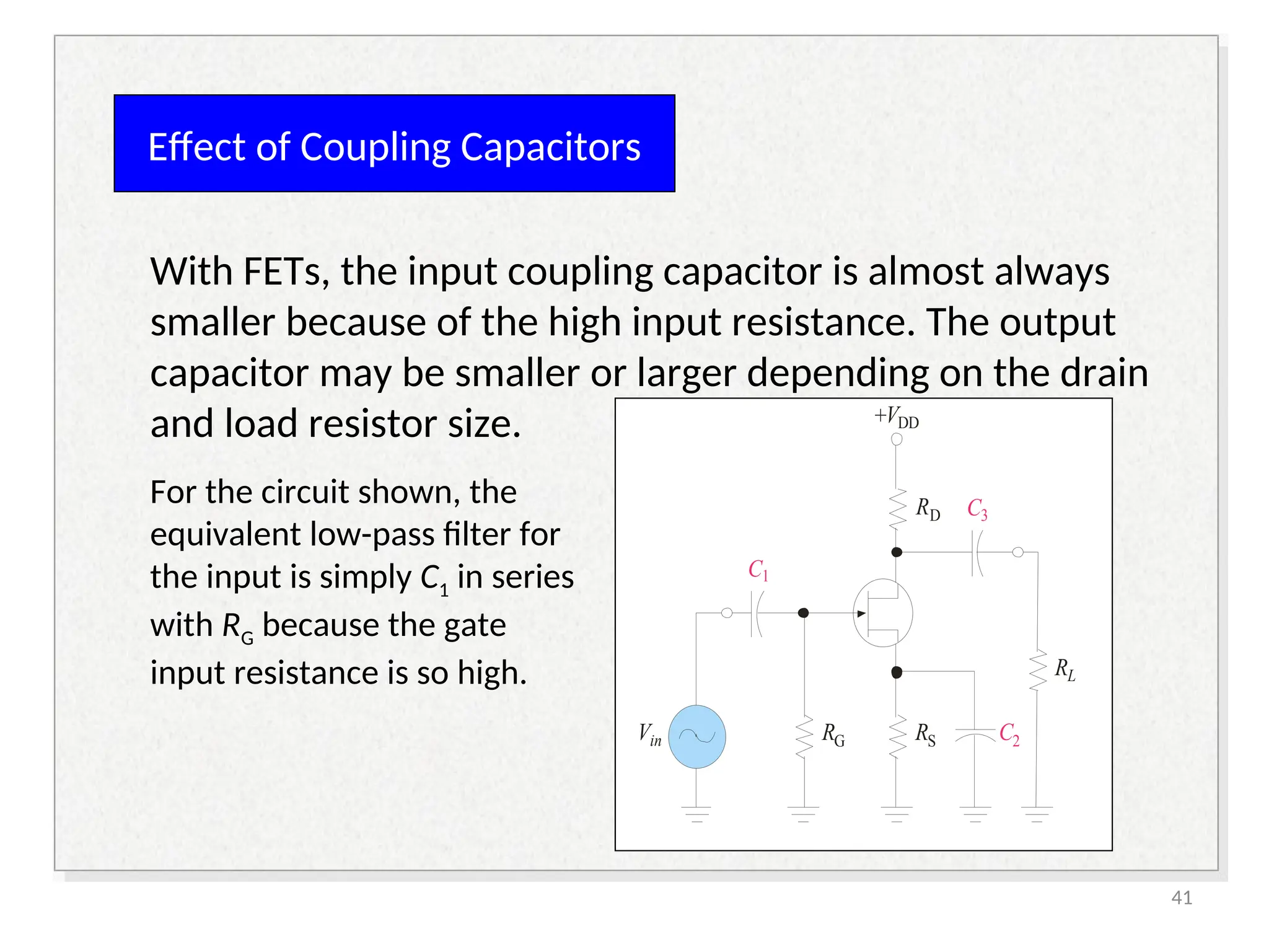
Effect of CouplingCapacitors
With FETs, the input coupling capacitor is almost always
smaller because of the high input resistance. The output
capacitor may be smaller or larger depending on the drain
and load resistor size.
RD
+VDD
RG
Vin RS
RL
C3
C1
C2
For the circuit shown, the
equivalent low-pass filter for
the input is simply C1 in series
with RG because the gate
input resistance is so high.
41
42.
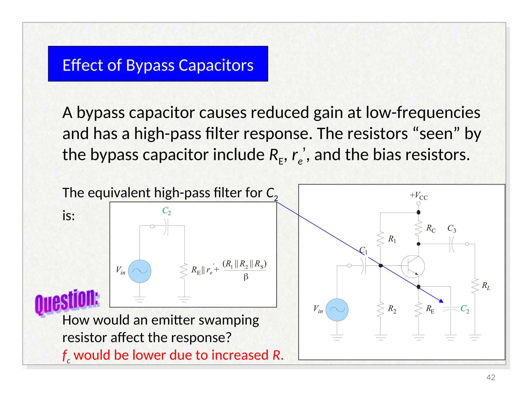
Effect of BypassCapacitors
A bypass capacitor causes reduced gain at low-frequencies
and has a high-pass filter response. The resistors “seen” by
the bypass capacitor include RE, re’, and the bias resistors.
RC
+VCC
R2
Vin
R1
RE
RL
C1
C3
2
C
The equivalent high-pass filter for C2
is:
How would an emitter swamping
resistor affect the response?
fc would be lower due to increased R.
RE
Vin
C2
|| r +
e
' R R R
( || || )
1 2 S
b
42