This document discusses the h-parameter model for BJTs. It provides the following key points:
1. The h-parameter model represents a BJT with real numbers that are easy to measure and use for circuit analysis. The model depicts the transistor's input impedance (hie), current gain (hfe), and output impedance (hoe).
2. For common-emitter mode, the h-parameter equivalent circuit shows the base as terminal 1, collector as terminal 2, and emitter as terminal 3. It models the relationships between base current and voltage (ib and VBE) and collector current and voltage (ic and VCE).
3. The h-parameter model is best
Fuzzy Logic Controlled Harmonic Suppressor in Cascaded Multilevel InverterIJPEDS-IAES
This paper presents an investigation of seven level cascaded H-bridge (CHB)
inverter in power system for compensation of harmonics. For power quality
control a Fuzzy Logic Control (FLC) giving comparatively better harmonic
reduction than the conventional controllers. Harmonic distortion is the most
important power quality problem stirring in multilevel inverter; the
harmonics can be eliminated by an optimal selection of switching angles. A
hybrid evaluation technique evaluates the obtained optimal switching angles
that are attained from the fuzzy inference system as well as neural network.
The proposed method will be implemented in MATLAB working platform
and the harmonic elimination performance will be evaluated.
Design and minimization of reversible programmable logic arrays and its reali...Sajib Mitra
Reversible computing dissipates zero energy in terms of information loss at input and also it can detect error of circuit by keeping unique input-output mapping. In this paper, we have proposed a cost effective design of Reversible Programmable Logic Arrays (RPLAs) which is able to realize multi-output ESOP (Exclusive-OR Sum-Of-Product) functions by using a cost effective 3×3 reversible gate, called MG (MUX Gate). Also a new algorithm has been proposed for the calculation of critical path delay of reversible PLAs. The minimization processes consist of algorithms for ordering of output functions followed by the ordering of products. Five lower bounds on the numbers of gates, garbage and quantum costs of reversible PLAs are also proposed. Finally, we have compared the efficiency of proposed design with the existing one by providing benchmark functions analysis. The experimental results show that the proposed design outperforms the existing one in terms of numbers of gates, garbage, quantum costs and delay.
International Journal of Engineering Research and Applications (IJERA) is an open access online peer reviewed international journal that publishes research and review articles in the fields of Computer Science, Neural Networks, Electrical Engineering, Software Engineering, Information Technology, Mechanical Engineering, Chemical Engineering, Plastic Engineering, Food Technology, Textile Engineering, Nano Technology & science, Power Electronics, Electronics & Communication Engineering, Computational mathematics, Image processing, Civil Engineering, Structural Engineering, Environmental Engineering, VLSI Testing & Low Power VLSI Design etc.
Direct Design of Reversible Combinational and Sequential Circuits Using PSDRM...IJRES Journal
Reversible logic will be a favourable logic by dissipating less heat than the thermo dynamic limit for
the emerging computing technologies. Also it has become very promising for low power designs. Reversible
designs of Combinational and Sequential circuits are built by replacing the latches, flip-flops and associated
combinational gates of the traditional irreversible designs by their reversible counter parts. But this replacement
technique is not very promising because it leads to high quantum cost and garbage outputs. So, in this paper we
presented both the direct design and replacement designs of 5-bit up down counter and universal shift register
which are practically important using reversible logic and PSDRM expressions. Replacement design is done by
replacing the RTL design using reversible designs. Direct design is done by representing the state transitions and
the output functions of the circuits using PSDRM expressions which are obtained from truth table or state
transition table. Thus my direct design of a 5-bit updown counter and universal shift register save 42.66%,
9.79% quantum cost and 93.75%, 40% garbage outputs respectively than the replacement design.
Minimum Mismatch of Current in Fully Differential Charge Pump for Integer N- ...IJERA Editor
Fully Differential ended charge pump (FDCP) are proven to have advantages over single ended charge pump at the cost of complexity and required more power for implementation for digital phase locked loop(DPLL). Wide swing cascodebias voltage with the rail to rail operational amplifier(opamp) as common mode feedback(CMFB) provides efficient solutions for current mismatch due to its non-idealities. The FDCP is simulated across process corners using 65nm technology with tsmc foundry for10Ghz DPLL. The power consumption of FDCP is 23mW with 100uA as Charge Pump (CP) current.
Comparative Study of Low Power Low Area Bypass Multipliers for Signal Process...IJERA Editor
This paper presents a comparative study of 1-dimensional bypassing multipliers on basis of delay, area and power. If we can reduce the power consumption of the multiplier block, then we can reduce the power consumption of various digital signal processing chips and communication systems. In 2-dimensional bypass multiplier is presented the effective analysis of Slices, Lut, Cost & area is achieved. The implementation of Braun multipliers and its bypassing techniques is done using Verilog HDL using Xilinx 12.4 ISE. Results are showed and it is verified using the Spartan-3E and Synopsys respectively.
A Low power and area efficient CLA adder design using Full swing GDI techniqueIJERA Editor
The low power VLSI design has an important role in designing of many electronic systems. While designing
any combinational or sequential circuits, the important parameters like power consumption, implementation
area, voltage leakage and performance of the circuit are to be considered. Design of area, high speed and powerefficient
data path logic systems forms the largest areas of research in VLSI system design. This paper presents
a low power Carry look ahead adder design using Full swing Gate diffusion (FS-GDI) technique. The proposed
CLA implementation utilizes improved full-swing GDI F1 and F2 gates, which are the counterparts of standard
CMOS NAND and NOR gates. The basic Gate Diffusion Input (GDI) logic style suffers from some practical
limitations like swing degradation, fabrication complexity in standard CMOS process and bulk connections.
These limitations can be overcome by Full swing GDI technique. The proposed technique utilizes a single swing
restoration (SR) transistor to improve the output swing of F1 and F2 GDI gates. A 16-bit CLA is designed and
Simulations are performed by Mentor graphics 130nm CMOS technology ELDO simulator. Simulation results
have shown a greater reduction in delay, power dissipation and area.
K-band waveguide T-junction diplexer for satellite communicationTELKOMNIKA JOURNAL
Design and measurement of two waveguide diplexers on H-plane T-junction, are presented.
The two diplexers structures consist of a waveguide H-plane T-junction and two waveguide obtained cavity
filters. The two diplexers operate in the same frequency bands (17 GHz-19.5 GHz). The simulation results
show that over the operating band of two filters, the return losses are better than 18 dB and insertion
losses are lower than 0.05 dB. The proposed diplexers have been simulated using Mician μ Wave Wizard
simulator based on the mode matching method (MMM). The diplexers have been validated experimentally
and results are presented. Simulated and measured results show good agreement.
Power Optimization using Reversible Gates for Booth’s MultiplierIJMTST Journal
Reversible logic attains the attraction of researchers in the last decade mainly due to low-power dissipation. Designers’ endeavours are thus continuing in creating complete reversible circuits consisting of reversible gates. This paper presents a design methodology for the realization of Booth’s multiplier in reversible mode. So that power is optimised Booth’s multiplier is considered as one of the fastest multipliers in literature and we have shown an efficient design methodology in reversible paradigm. The proposed architecture is capable of performing both signed and unsigned multiplication of two operands without having any feedbacks, whereas existing multipliers in reversible mode consider loop which is strictly prohibited in reversible logic design. Theoretical underpinnings, established for the proposed design, show that the proposed circuit is very efficient from reversible circuit design point of view.
IJERA (International journal of Engineering Research and Applications) is International online, ... peer reviewed journal. For more detail or submit your article, please visit www.ijera.com
IJRET : International Journal of Research in Engineering and Technology is an international peer reviewed, online journal published by eSAT Publishing House for the enhancement of research in various disciplines of Engineering and Technology. The aim and scope of the journal is to provide an academic medium and an important reference for the advancement and dissemination of research results that support high-level learning, teaching and research in the fields of Engineering and Technology. We bring together Scientists, Academician, Field Engineers, Scholars and Students of related fields of Engineering and Technology.
International Journal of Engineering Research and Applications (IJERA) is an open access online peer reviewed international journal that publishes research and review articles in the fields of Computer Science, Neural Networks, Electrical Engineering, Software Engineering, Information Technology, Mechanical Engineering, Chemical Engineering, Plastic Engineering, Food Technology, Textile Engineering, Nano Technology & science, Power Electronics, Electronics & Communication Engineering, Computational mathematics, Image processing, Civil Engineering, Structural Engineering, Environmental Engineering, VLSI Testing & Low Power VLSI Design etc.
Evolution of Structure of Some Binary Group-Based N-Bit Compartor, N-To-2N De...VLSICS Design
Reversible logic has attracted substantial interest due to its low power consumption which is the main
concern of low power VLSI systems. In this paper, a novel 4x4 reversible gate called inventive gate has
been introduced and using this gate 1-bit, 2-bit, 8-bit, 32-bit and n-bit group-based reversible comparator
have been constructed with low value of reversible parameters. The MOS transistor realizations of 1-bit, 2-
bit, and 8-bit of reversible comparator are also presented and finding power, delay and power delay
product (PDP) with appropriate aspect ratio W/L. Novel inventive gate has the ability to use as an n-to-2n
decoder. Different novel reversible circuit design style is compared with the existing ones. The relative
results shows that the novel reversible gate wide utility, group-based reversible comparator outperforms
the present style in terms of number of gates, garbage outputs and constant input.
Compact low power high slew-rate cmos buffer amplifier with power gating tech...VLSICS Design
A qualitative analysis of different parameters such as Phase noise, Slew rate and tranconductance by using
power gating reduction technique is presented. The circuit achieves the large driving capability by
employing simple comparators to sense the transients of the input to turn on the output stages, which are
statically off in the stable state. The effect of the different number of transistors and their topologies on the
phase noise and Slew rate is analyzed. Good agreement between qualitative and quantitative measurements
is observed. Scope of reducing of Noise and avoidance of Leakage due to various sources is discussed.
Low Power Implementation of Booth’s Multiplier using Reversible GatesIJMTST Journal
Reversible logic attains the attraction of researchers in the last decade mainly due to low-power dissipation. Designers’ endeavours are thus continuing in creating complete reversible circuits consisting of reversible gates. This paper presents a design methodology for the realization of Booth’s multiplier in reversible mode. So that power is optimised Booth’s multiplier is considered as one of the fastest multipliers in literature and we have shown an efficient design methodology in reversible paradigm. The proposed architecture is capable of performing both signed and unsigned multiplication of two operands without having any feedbacks, whereas existing multipliers in reversible mode consider loop which is strictly prohibited in reversible logic design. Theoretical underpinnings, established for the proposed design, show that the proposed circuit is very efficient from reversible circuit design point of view.
EVOLUTION OF STRUCTURE OF SOME BINARY GROUP-BASED N-BIT COMPARATOR, N-TO-2N D...VIT-AP University
Reversible logic has attracted substantial interest due to its low power consumption which is the main concern of low power VLSI circuit design. In this paper, a novel 4x4 reversible gate called inventive gate has been introduced and using this gate 1-bit, 2-bit, 8-bit, 32-bit and n-bit group-based reversible comparator have been constructed with low value of reversible parameters. The MOS transistor realizations of 1-bit, 2- bit, and 8-bit of reversible comparator are also presented and finding power, delay and power delay product (PDP) with appropriate aspect ratio W/L. Novel inventive gate has the ability to use as an n-to-2n decoder. Different proposed novel reversible circuit design style is compared with the existing ones. The relative results shows that the novel reversible gate wide utility, group-based reversible comparator outperforms the present design style in terms of number of gates, garbage outputs and constant input.
BJT small signal model – Analysis of CE, CB, CC amplifiers- Gain and frequency response – MOSFET small signal model– Analysis of CS and Source follower – Gain and frequency response- High frequency analysis.
Harmonic elimination at the fundamental frequency is very much appropriate for high and medium range of power generation and applications. This paper considers a new technique for selective harmonic elimination (SHE), in which the total harmonic distortion (THD) is minimized when compared with that of the conventional one. With this technique, the harmonics at lower order are eliminated, which are more predominant than the higher ones.Cascaded H-Bridge inverter fed by a single DC is considered which is simulated with the switching angles generated by both the conventional method of SHE and the new method of SHE. The simulated results of the load voltage and the waveforms of the harmonic analysis are shown. The THD values are compared for the two techniques. The experimental results are also shown for the new technique. The switching angles are generated with the help of field programmable gated array (FPGA) in the hardware. The value of experimental THD of voltage is compared with that of simulated THD and the comparison prove that the results are satisfactory.
Ece 523 project – fully differential two stage telescopic op ampKarthik Rathinavel
• Designed a two stage op-amp with first stage as a telescopic amplifier and second stage being a common source, in Cadence.
• Simulated the loop characteristics of the amplifier to have atleast 100 MHz Unity Gain Bandwidth, 65 dB gain and 60º phase margin (both differential loop and Common Mode) for three temperature (27,-40,100) corners.
• Extracted the layout of the design in Virtuoso (after passing DRC an LVS) and simulated the differential loop performances of the extracted netlist.
• Designed a third order Butterworth filter with 100 KHz corner frequency using the op-amp.
I presented this slid in my last presentation about bipolar junction transistor configuration.Now I'm sharing this with all of you guys it can be helpful for you.
Look at the beautiful view of forgiveness of mistakes.
Thank you
A Two Channel Analog Front end Design AFE Design with Continuous Time ∑-∆ Mod...IJECEIAES
In this context, the AFE with 2-channels is described, which has high impedance for low power application of bio-medical electrical activity. The challenge in obtaining accurate recordings of biomedical signals such as EEG/ECG to study the human body in research work. This paper is to propose Multi-Vt in AFE circuit design cascaded with CT modulator. The new architecture is anticipated with two dissimilar input signals filtered from 2-channel to one modulator. In this methodology, the amplifier is low powered multi-VT Analog Front-End which consumes less power by applying dual threshold voltage. Type -I category 2 channel signals of the first mode: 50 and 150 Hz amplified from AFE are given to 2nd CT sigmadelta ADC. Depict the SNR and SNDR as 63dB and 60dB respectively, consuming the power of 11mW. The design was simulated in a 0.18 um standard UMC CMOS process at 1.8V supply. The AFE measured frequency response from 50 Hz to 360 Hz, depict the SNR and SNDR as 63dB and 60dB respectively, consuming the power of 11mW. The design was simulated in 0.18 m standard UMC CMOS process at 1.8V supply. The AFE measured frequency response from 50 Hz to 360 Hz, programmable gains from 52.6 dB to 72 dB, input referred noise of 3.5 µV in the amplifier bandwidth, NEF of 3.
Design and simulation of high frequency colpitts oscillator based on BJT ampl...IJECEIAES
Frequency oscillator is one of the basic devices that can be used in most electrical, electronics and communications circuits and systems. There are many types of oscillators depending on frequency range used in an application such as audio, radio and microwave. The needed was appeared to use high and very high frequencies to make the rapid development of advanced technology Colpitts oscillator is one of the most common types of oscillator, it can be used for radio frequency (RF), that its output signal is often utilized at the basic of a wireless communication system in most application. In this research, a Colpitts oscillator is comprised from a bipolar junction transistor (BJT) amplifier with LC tank. This design is carrying out with a known Barkhausen criterion for oscillation. Firstly, is carried out using theoretical calculation. The secondary is carried out using simulation (Multisim 13). All the obtained result from the above two approaches are 10 MHz and 9.745 MHz respectively. This result is seen to be very encouraging.
Multilevel inverters are emerging as the new breed of power converter options for high power applications. They typically synthesis the staircase voltage waveform (from several dc sources) which reduced harmonic content. This paper presents a simple selective harmonic elimination (SHE) modulation for single-phase cascaded H-bridge (CHB) multilevel inverter. The optimum switching angle of the transcendental equations describing the fundamental and harmonic components is solved by means of the Newton-Raphson (NR) method. The proposed SHE scheme is performed through simulation using MATLAB/Simulink. This simulation results are then verified through experiment using Altera DE0-Nano field-programmable gate array (FPGA). The proposed SHE is efficient in eliminating the lowest-order harmonics and producing a higher quality output waveform with a better harmonic profile.
Improved power quality buck boost converter for SMPSIJECEIAES
In this paper, a Neural Network (NN) controlled Buck-Boost Converter (BBC) based Switched Mode Power Supply (SMPS) for a PC application is proposed. The proposed BBC is analyzed, modeled and designed for the rated load. Generally, the utilization of Multiple Output SMPS (MOSMPS) for PC application introduces Power Quality (PQ) issues in the power system network. Unlike conventional SMPS the proposed NN controlled BBC can accomplish improvement of power quality. The NN controller reduces the Total Harmonic Distortion (THD) of source current below 5%, maintains input side Power Factor (PF) to be nearly unity and improves the output voltage regulation. In the proposed system, NN controller replaces the conventional PI controller and overcomes the drawbacks of the conventional system. The proposed BBC is validated adopting MATLAB/SIMULINK software. The simulation analysis validate that the proposed NN controlled BBC performs better than conventional converter in terms of PQ indices under fluctuating conditions.
Cosmetic shop management system project report.pdfKamal Acharya
Buying new cosmetic products is difficult. It can even be scary for those who have sensitive skin and are prone to skin trouble. The information needed to alleviate this problem is on the back of each product, but it's thought to interpret those ingredient lists unless you have a background in chemistry.
Instead of buying and hoping for the best, we can use data science to help us predict which products may be good fits for us. It includes various function programs to do the above mentioned tasks.
Data file handling has been effectively used in the program.
The automated cosmetic shop management system should deal with the automation of general workflow and administration process of the shop. The main processes of the system focus on customer's request where the system is able to search the most appropriate products and deliver it to the customers. It should help the employees to quickly identify the list of cosmetic product that have reached the minimum quantity and also keep a track of expired date for each cosmetic product. It should help the employees to find the rack number in which the product is placed.It is also Faster and more efficient way.
Water scarcity is the lack of fresh water resources to meet the standard water demand. There are two type of water scarcity. One is physical. The other is economic water scarcity.
Explore the innovative world of trenchless pipe repair with our comprehensive guide, "The Benefits and Techniques of Trenchless Pipe Repair." This document delves into the modern methods of repairing underground pipes without the need for extensive excavation, highlighting the numerous advantages and the latest techniques used in the industry.
Learn about the cost savings, reduced environmental impact, and minimal disruption associated with trenchless technology. Discover detailed explanations of popular techniques such as pipe bursting, cured-in-place pipe (CIPP) lining, and directional drilling. Understand how these methods can be applied to various types of infrastructure, from residential plumbing to large-scale municipal systems.
Ideal for homeowners, contractors, engineers, and anyone interested in modern plumbing solutions, this guide provides valuable insights into why trenchless pipe repair is becoming the preferred choice for pipe rehabilitation. Stay informed about the latest advancements and best practices in the field.
Hybrid optimization of pumped hydro system and solar- Engr. Abdul-Azeez.pdffxintegritypublishin
Advancements in technology unveil a myriad of electrical and electronic breakthroughs geared towards efficiently harnessing limited resources to meet human energy demands. The optimization of hybrid solar PV panels and pumped hydro energy supply systems plays a pivotal role in utilizing natural resources effectively. This initiative not only benefits humanity but also fosters environmental sustainability. The study investigated the design optimization of these hybrid systems, focusing on understanding solar radiation patterns, identifying geographical influences on solar radiation, formulating a mathematical model for system optimization, and determining the optimal configuration of PV panels and pumped hydro storage. Through a comparative analysis approach and eight weeks of data collection, the study addressed key research questions related to solar radiation patterns and optimal system design. The findings highlighted regions with heightened solar radiation levels, showcasing substantial potential for power generation and emphasizing the system's efficiency. Optimizing system design significantly boosted power generation, promoted renewable energy utilization, and enhanced energy storage capacity. The study underscored the benefits of optimizing hybrid solar PV panels and pumped hydro energy supply systems for sustainable energy usage. Optimizing the design of solar PV panels and pumped hydro energy supply systems as examined across diverse climatic conditions in a developing country, not only enhances power generation but also improves the integration of renewable energy sources and boosts energy storage capacities, particularly beneficial for less economically prosperous regions. Additionally, the study provides valuable insights for advancing energy research in economically viable areas. Recommendations included conducting site-specific assessments, utilizing advanced modeling tools, implementing regular maintenance protocols, and enhancing communication among system components.
Immunizing Image Classifiers Against Localized Adversary Attacksgerogepatton
This paper addresses the vulnerability of deep learning models, particularly convolutional neural networks
(CNN)s, to adversarial attacks and presents a proactive training technique designed to counter them. We
introduce a novel volumization algorithm, which transforms 2D images into 3D volumetric representations.
When combined with 3D convolution and deep curriculum learning optimization (CLO), itsignificantly improves
the immunity of models against localized universal attacks by up to 40%. We evaluate our proposed approach
using contemporary CNN architectures and the modified Canadian Institute for Advanced Research (CIFAR-10
and CIFAR-100) and ImageNet Large Scale Visual Recognition Challenge (ILSVRC12) datasets, showcasing
accuracy improvements over previous techniques. The results indicate that the combination of the volumetric
input and curriculum learning holds significant promise for mitigating adversarial attacks without necessitating
adversary training.
Saudi Arabia stands as a titan in the global energy landscape, renowned for its abundant oil and gas resources. It's the largest exporter of petroleum and holds some of the world's most significant reserves. Let's delve into the top 10 oil and gas projects shaping Saudi Arabia's energy future in 2024.
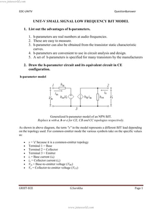
1. EDC-UNITV Question&answer
GRIET-ECE G.Surekha Page 1
UNIT-V SMALL SIGNAL LOW FREQUENCY BJT MODEL
1. List out the advantages of h-parameters.
1. h-parameters are real numbers at audio frequencies.
2. These are easy to measure.
3. h-parameter can also be obtained from the transistor static characteristic
curves.
4. h-parameters are convenient to use in circuit analysis and design.
5. A set of h-parameters is specified for many transistors by the manufacturers
2. Draw the h-parameter circuit and its equivalent circuit in CE
configuration.
h-parameter model
Generalized h-parameter model of an NPN BJT.
Replace x with e, b or c for CE, CB and CC topologies respectively.
As shown in above diagram, the term "x" in the model represents a different BJT lead depending
on the topology used. For common-emitter mode the various symbols take on the specific values
as:
x = 'e' because it is a common-emitter topology
Terminal 1 = Base
Terminal 2 = Collector
Terminal 3 = Emitter
ii = Base current (ib)
io = Collector current (ic)
Vin = Base-to-emitter voltage (VBE)
Vo = Collector-to-emitter voltage (VCE)
www.jntuworld.com
www.jntuworld.com
2. EDC-UNITV Question&answer
GRIET-ECE G.Surekha Page 2
and the h-parameters are given by:
hie – The input impedance of the transistor (corresponding to the emitter resistance re).
hre – Represents the dependence of the transistor's IB–VBE curve on the value of VCE. It is
usually very small and is often neglected (assumed to be zero).
hfe – The current-gain of the transistor. This parameter is often specified as hFE or the DC
current-gain (βDC) in datasheets.
hoe – The output impedance of transistor. This term is usually specified as an admittance
and has to be inverted to convert it to an impedance.
For the CE topology, an approximate h-parameter model is commonly used which further
simplifies the circuit analysis. For this the hoe and hre parameters are neglected (that is, they are
set to infinity and zero, respectively). It should also be noted that the h-parameter model as
shown is suited to low-frequency, small-signal analysis. For high-frequency analysis the inter-
electrode capacitances that are important at high frequencies must be added.
3. Summarize salient features of characteristics of BJT operating in CE, CB, CC configurations.
COMPARISON OF CB, CE, CC CONFIGURATIONS:
www.jntuworld.com
www.jntuworld.com
3. EDC-UNITV Question&answer
GRIET-ECE G.Surekha Page 3
S. No. Property CB CE CC
1 Input Resistance Low ( 100 ) Moderate( 750 ) High ( 750k )
2 Output resistance High ( 450k) Moderate ( 45k) Low ( 75 )
3 Current gain 1 High High
4 Voltage gain 150 500 < 1
5 Phase shift between
input and output
voltages
0 or 360 180 0 or 360
6 Applications High frequency
circuits
AF circuits Impedance
matching.
www.jntuworld.com
www.jntuworld.com