Downloaded 168 times


![Thus,
Aq = I*W / DB*P'(0) ……………………(2)
Equating both the equations :-
2QB/P'(0)*W = I*W/DB*P(O)
QB = I*W2/2DB ………………………....(3)
Finally,The static diffusion capacitance
Cde=dQB/dV
From above equation:-
Cde = dI*W2/ 2DB*Dv
= [W2/ re *2DB]
Where
re = emitter junction incremental resistance and is given by :-
re=dV/dl = VT/IE](https://image.slidesharecdn.com/hybridmodelanalogelectronics-151021095155-lva1-app6891/75/Hybrid-model-analog-electronics-26-2048.jpg)
![Thus ,
Cde=[W2/2DB].[IE/VT]
Cde=gm.[W2/2DB] = Ce
This indicates that the Cde is proportional to the IE
and inversely proportional with VT. Cde is almost
independent of temperature.
Experimentally, Ce is determined from a
measurement of the frequency flat which the CE
short-circuit current gain drops to unity ;
Ce =gm/2πft](https://image.slidesharecdn.com/hybridmodelanalogelectronics-151021095155-lva1-app6891/75/Hybrid-model-analog-electronics-27-2048.jpg)


![Looking at the above fig.we can write
IL= -gmVb’e
And
Ii= Vb’e [ gb’e + jw (Cc+ Ce) ]
Current gain under short circuit condition is
AI = IL/ Ii
, = -gmVb’e / Vb’e [gb’e + jw (Cc+Ce) ]
AI = -hfe/[1 + j2f(Cc+Ce)/ gb’e] ………..Eq.(1)
AI =- hfe/[1 + jf/fβ]](https://image.slidesharecdn.com/hybridmodelanalogelectronics-151021095155-lva1-app6891/75/Hybrid-model-analog-electronics-46-2048.jpg)
![AI becomes :
AI = 1= hfe/[1 +( fT/fβ)2 ] … eq.(3)
The ratio fT/ fβ, is quite large as compared to (fT/
fβ>>1)) hence Equation (1) becomes
1= hfe/ fT/fβ
substituting this value of
fβ= gm/ hfe2f(Cc+Ce)
therefore
fT = gm/2f(Cc+Ce) …. Eq.(4)](https://image.slidesharecdn.com/hybridmodelanalogelectronics-151021095155-lva1-app6891/75/Hybrid-model-analog-electronics-49-2048.jpg)


![As K = Vce/Vb’e
= ILRL/ Vb’e
= (-gmVb’e)RL/Vb’e
= -gmRL
So ;
1-K=1+ gmRL
Thus, AI = IL/ Ii
AI = -gmVb’e / Vb’e [gb’e + jwCeq ]](https://image.slidesharecdn.com/hybridmodelanalogelectronics-151021095155-lva1-app6891/75/Hybrid-model-analog-electronics-56-2048.jpg)
![As we know
gb’e= gm/hfe
Thus ,
Ai = -gb’ehfe/[gb’e+ jwCeq ]
Ai = -hfe/[1 + j2Πf(Ceq)/ gb’e] ………..Eq.(1)
Ai= - hfe/[1 + jf/fH]
fH= gb’e/ 2 Πceq
=1/ 2Πrb’e[Ce+Cc(1 +gmRL)]
The simplified equivalent circuit is at RL= 0 :-
fH=1/ 2Πrb’e(Ce+Cc)= f
So the current gain = Ai = hfe / [ 1+(f /fh)2]1/2
= hfe / (2)1/2,
= 0.707 hfe](https://image.slidesharecdn.com/hybridmodelanalogelectronics-151021095155-lva1-app6891/75/Hybrid-model-analog-electronics-57-2048.jpg)

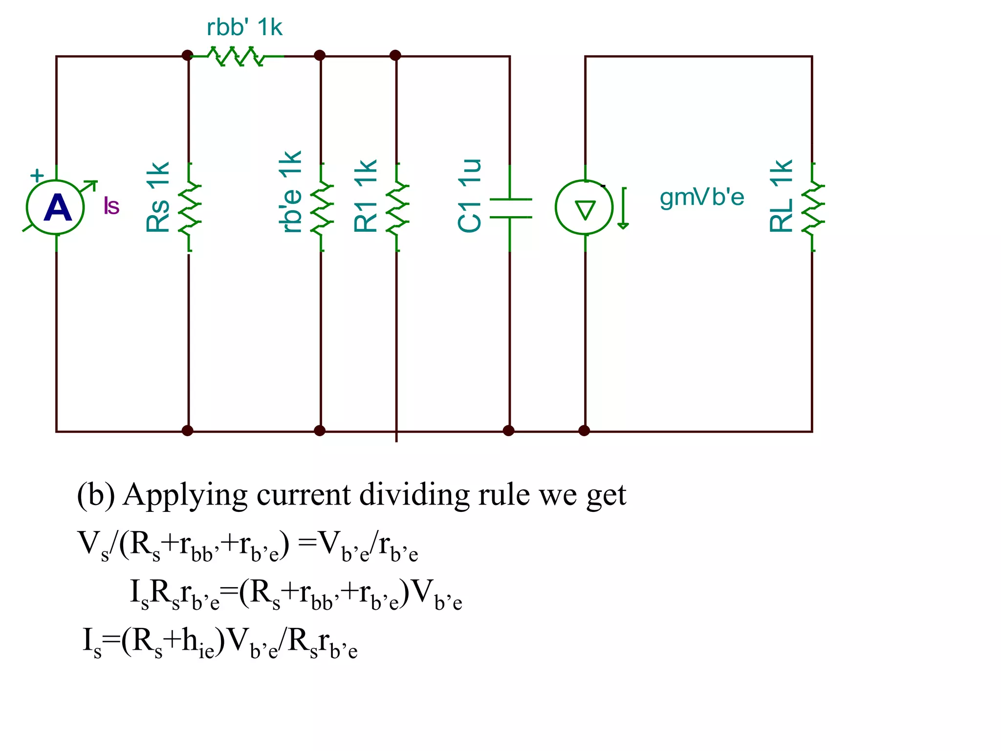
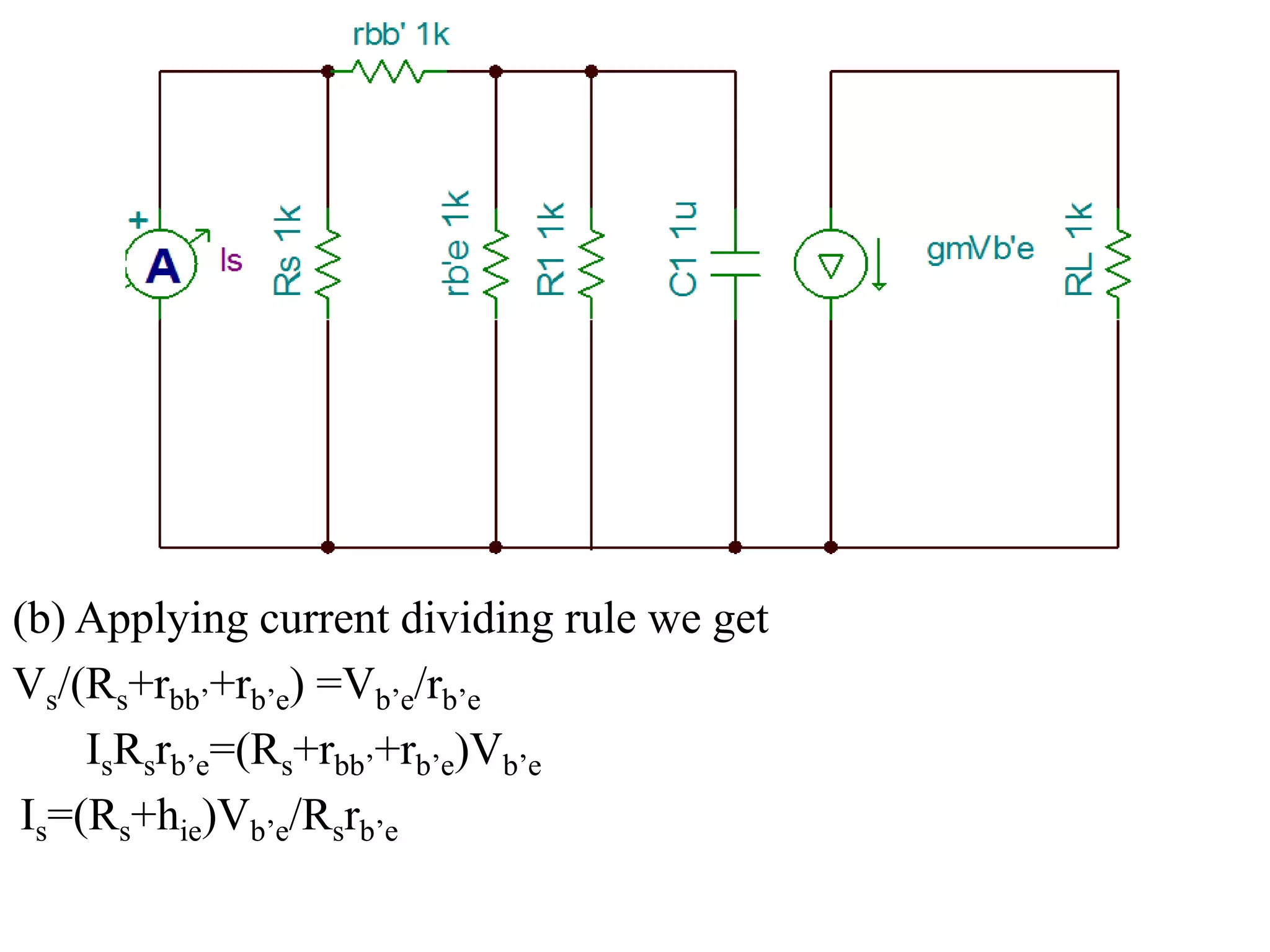
![Rs’=Rs+rbb’=1/Gs’
By applying KCL at B’ & C, we get : -
Gs’Vs=[Gs’+gb’e+s(Ce+Cc)]Vb’e-sCcVo..(1)
0=(gm-sCc)Vb’e+({1/RL}+sCc)Vo……(2)
We know that the voltage gain is
By solving the equation 2 and find the value of
And put I in equation 1
Avs=Vo/Vs
Vb’e
Vb’e = ({1/RL}+sCc)Vo /(sCc-gm)](https://image.slidesharecdn.com/hybridmodelanalogelectronics-151021095155-lva1-app6891/75/Hybrid-model-analog-electronics-59-2048.jpg)
![Vo/Vs= -Gs’RL(gm-sCc)/ s2CeCcRL +s[Ce+Cc+CcRL
(gm+gb’e+Gs’)]+Gs’+gb’e……eqn.(3)
By solving the quadratic equation
We get
Avs=Vo/Vs=K1(s-s0)/[(s-s1)(s-s2)…eqn.(4)
Where
K1=Gs’/Ce,
s0=gm/Cc
s1=Complex value
s2 =Complex value](https://image.slidesharecdn.com/hybridmodelanalogelectronics-151021095155-lva1-app6891/75/Hybrid-model-analog-electronics-60-2048.jpg)


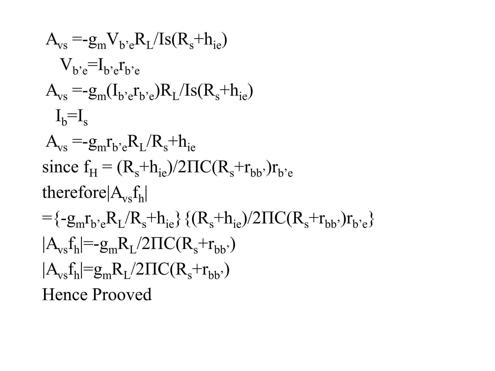
]/2Π(Ce+Cc)}
|Avsfh|={gmRL/2Π(Ce+Cc)}/{[(1+CcgmRL) /(Ce+Cc)
](Rs+rbb’)}
fT = gm/2Π(Ce+Cc)
|Avsfh|= fT RL/{(1+ 2ΠfTCcRL)(Rs+rbb’)}](https://image.slidesharecdn.com/hybridmodelanalogelectronics-151021095155-lva1-app6891/75/Hybrid-model-analog-electronics-65-2048.jpg)


![Voltage gain
A = Vo/Vi = Ve/Vi….............(1)
Ve=IZ
=I/(1/RL+jwCL)
=gmVb'e/((1+jwCLRL)/RL)
=gmRLVb'e/(1+jwCLRL)
=gmRL(Vi-Ve)/(1+jwCLRL)
Ve = gmRLVi/(1+jwCLRL)– gmRLVe /(1+jwCLRL )
Ve+VegmRL/(1+jwCLRL) =gmRLVi/(1+jwCLRL)
(Ve[(1+jwCLRL +gmRL)]) / (1
+jwCLRL)=gmRLVi/(1+jwCLRL)](https://image.slidesharecdn.com/hybridmodelanalogelectronics-151021095155-lva1-app6891/75/Hybrid-model-analog-electronics-75-2048.jpg)
![Therefore
Av=Vo/Vi
gmRL
1+gmRL+jwCLRL
Upper cut-off frequency fH
Av = gmRL/(1+gmRL)(1/1+[jwCLRL/(1+gmRL)])
gmRL
1+gmRL(1+jf/fH)
Thus ,
Av =AVL/(1+jf/fH)
Where ,
AVL=gmRL/1+gmRL<1
fH=1+gmRL/2ΠCLRL](https://image.slidesharecdn.com/hybridmodelanalogelectronics-151021095155-lva1-app6891/75/Hybrid-model-analog-electronics-76-2048.jpg)


]/2Π(Ce+Cc)}
|Avsfh|={gmRL/2Π(Ce+Cc)}/{[(1+CcgmRL) /(Ce+Cc) ](Rs+rbb’)}
fT = gm/2Π(Ce+Cc)
|Avsfh|= fT RL/{(1+ 2ΠfTCcRL)(Rs+rbb’)}
Hence Prooved](https://image.slidesharecdn.com/hybridmodelanalogelectronics-151021095155-lva1-app6891/75/Hybrid-model-analog-electronics-98-2048.jpg)
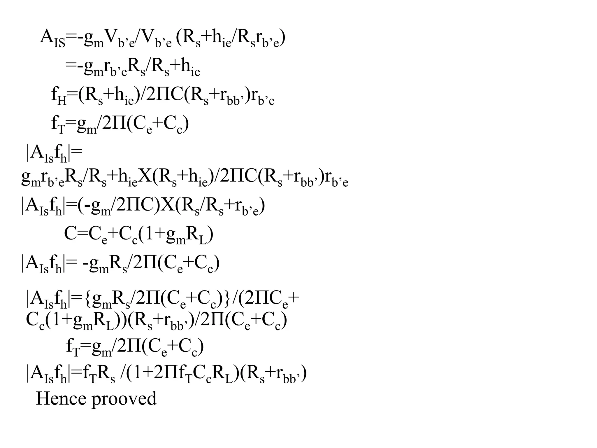


![AI={-gmgL/[gb’e (gce+gL+gb’c) +gb’c gm]}
dividing both num.&denom. by gb’e gL we get
AI={-gm/gb’e}/{[(gce+gL+gb’c)/gL]+[gb’c gm /gL]}
hfe=-gm/gb’e
gL= gm gb’c
AI=-hfe/{1+(gce+gb’c+gmgb’c)/gL}
AI = -hfe/(1+RLhoe )
Hence proved](https://image.slidesharecdn.com/hybridmodelanalogelectronics-151021095155-lva1-app6891/75/Hybrid-model-analog-electronics-107-2048.jpg)

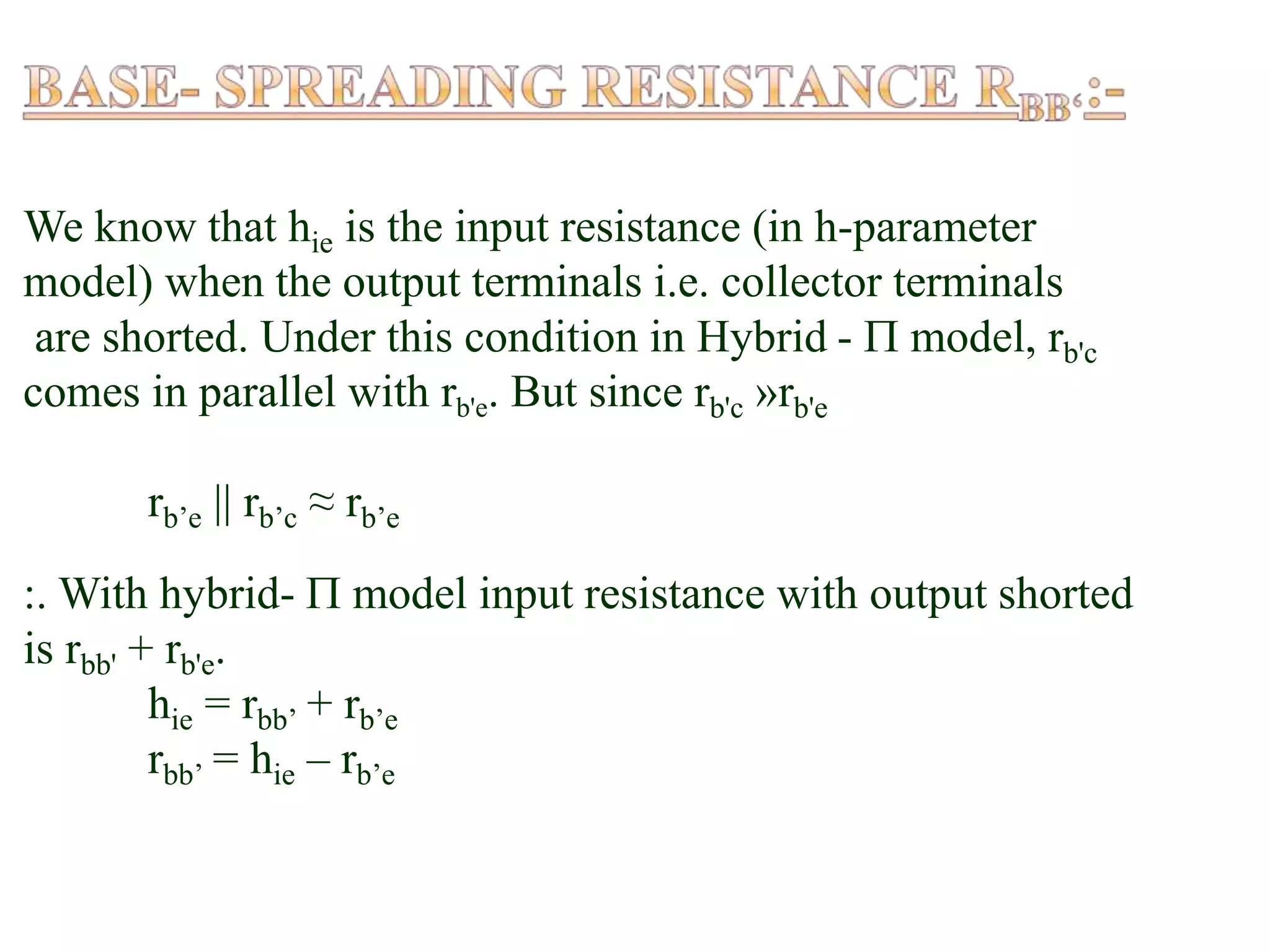
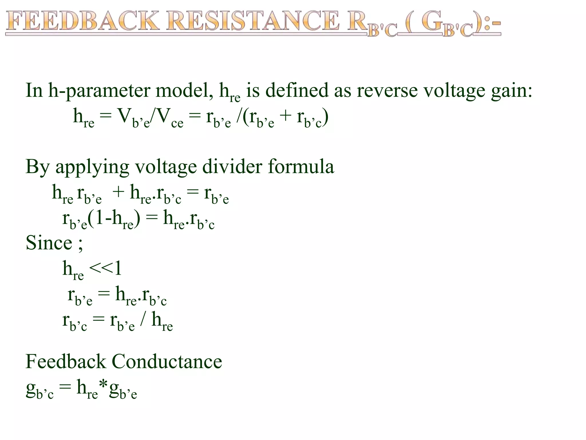
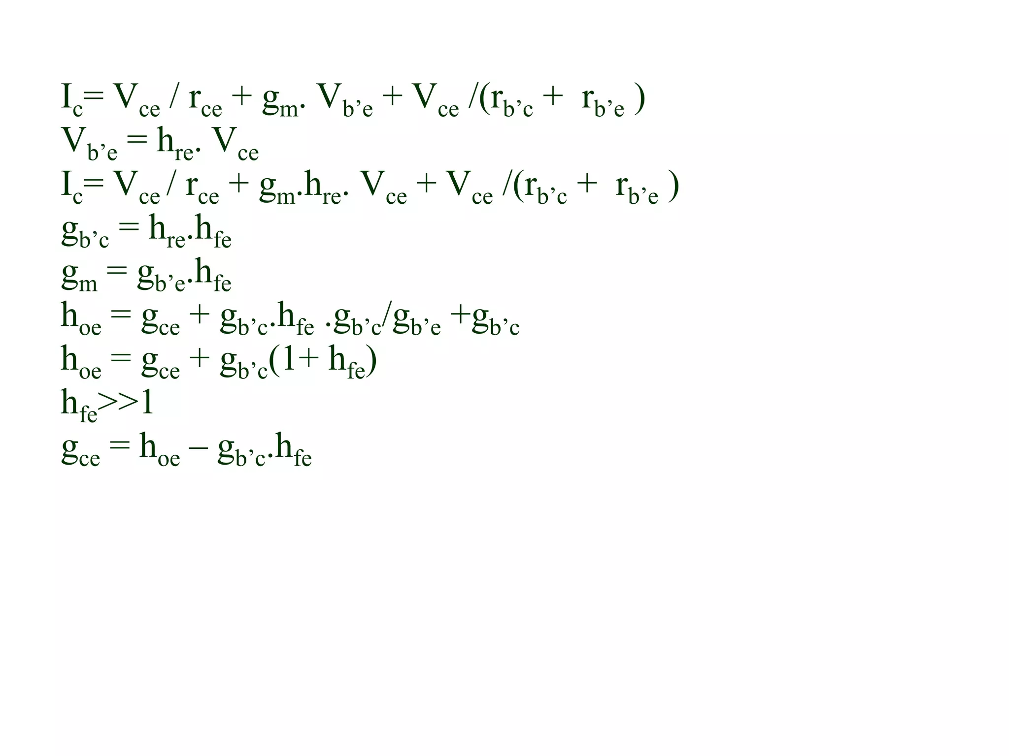
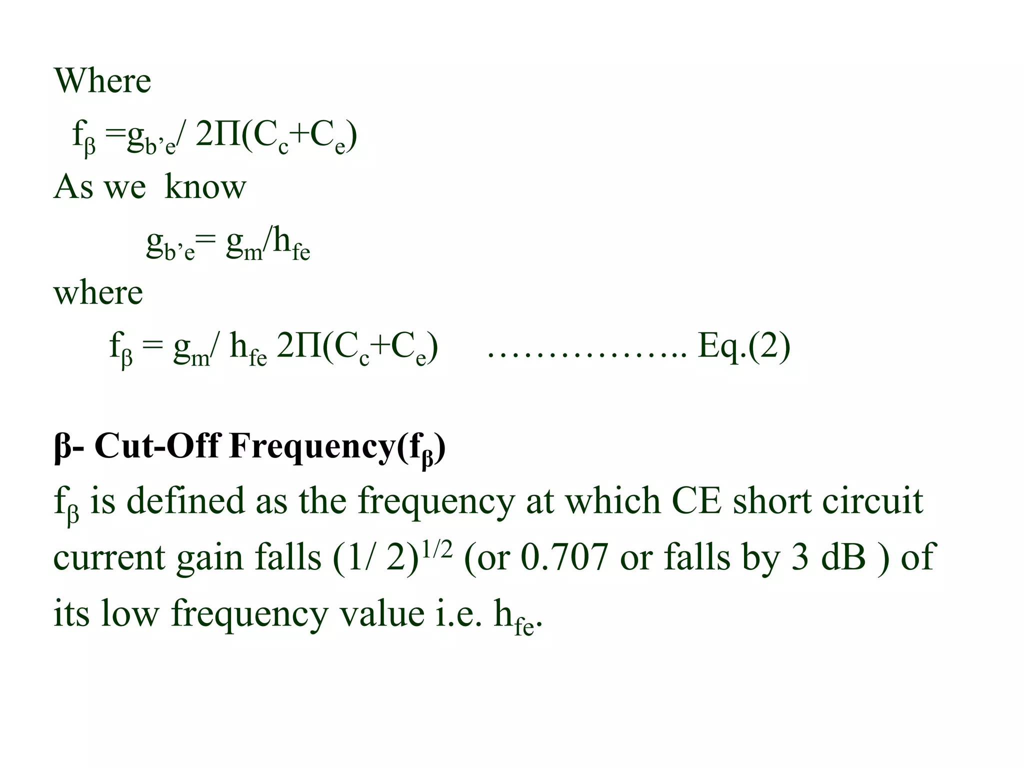
The document discusses the hybrid-π model used for high-frequency transistor analysis, highlighting its advantages of simplicity and accuracy. It explains how this model assumes all parameters are constant at high frequencies and delineates the mathematical derivations for transconductance and diffusion capacitance. Additionally, the document addresses frequency-related concepts such as cut-off frequencies and their implications on transistor performance.
Introduction to the hybrid model; dates indicating the presentation timeline.
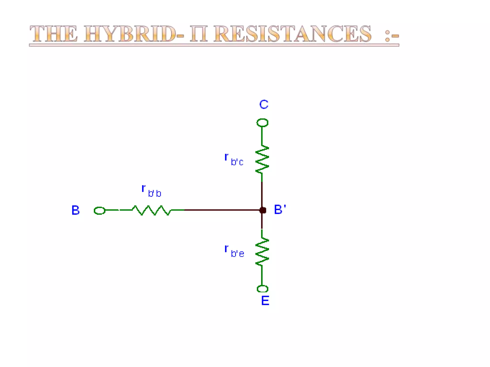
Describes the unsuitability of h-parameters for high frequency due to variable values and complexity.
Details advantages of the hybrid-π model, emphasizing its accuracy and simplicity for high frequency analysis.
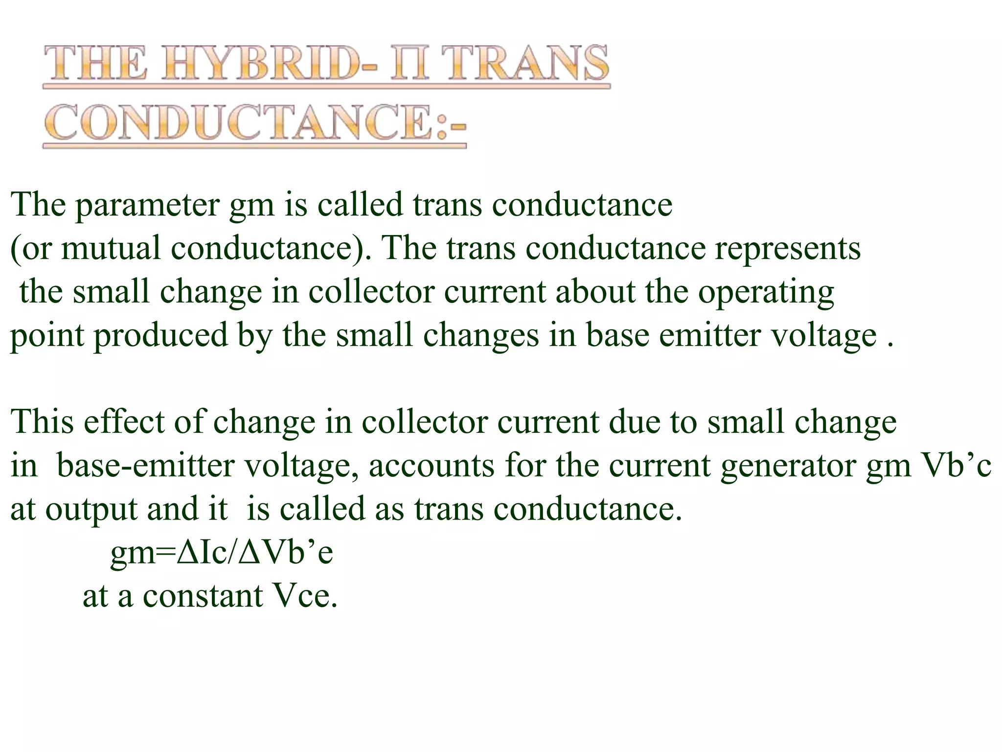
Definition and equations relating to transconductance, diffusion capacitance, and their interdependencies.
Discusses the capacitive effects at high frequencies and their impact on transistor performance.
Describes how the hybrid-π model incorporates low frequency parameters and feedback conductance.
Calculates current gain and cut-off frequency for transistors under different configurations.
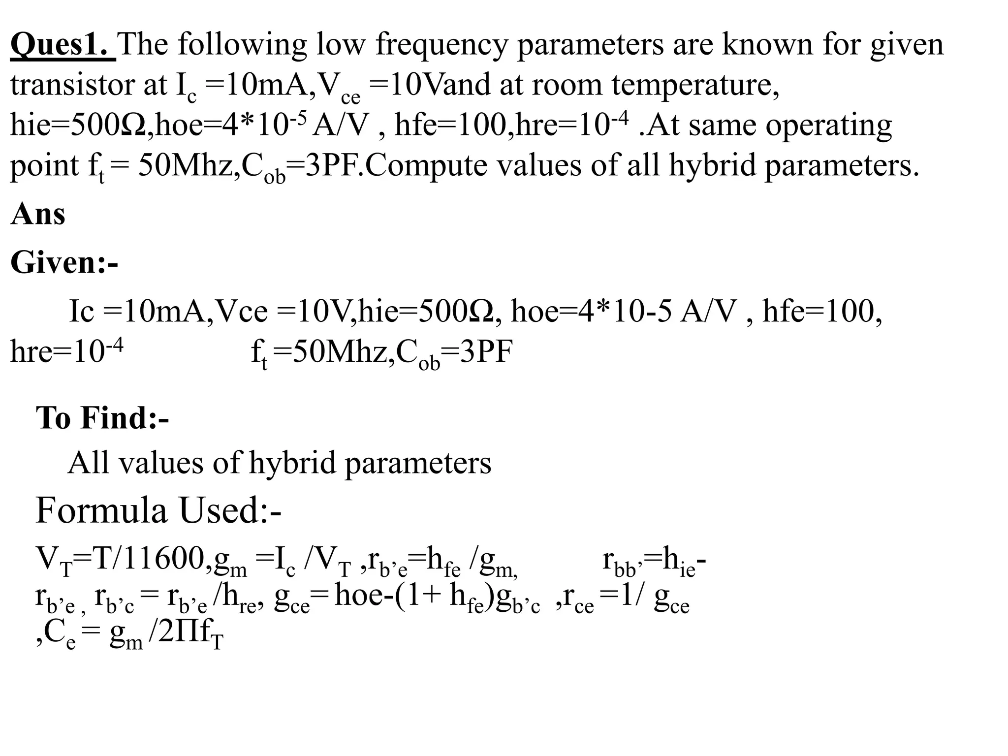
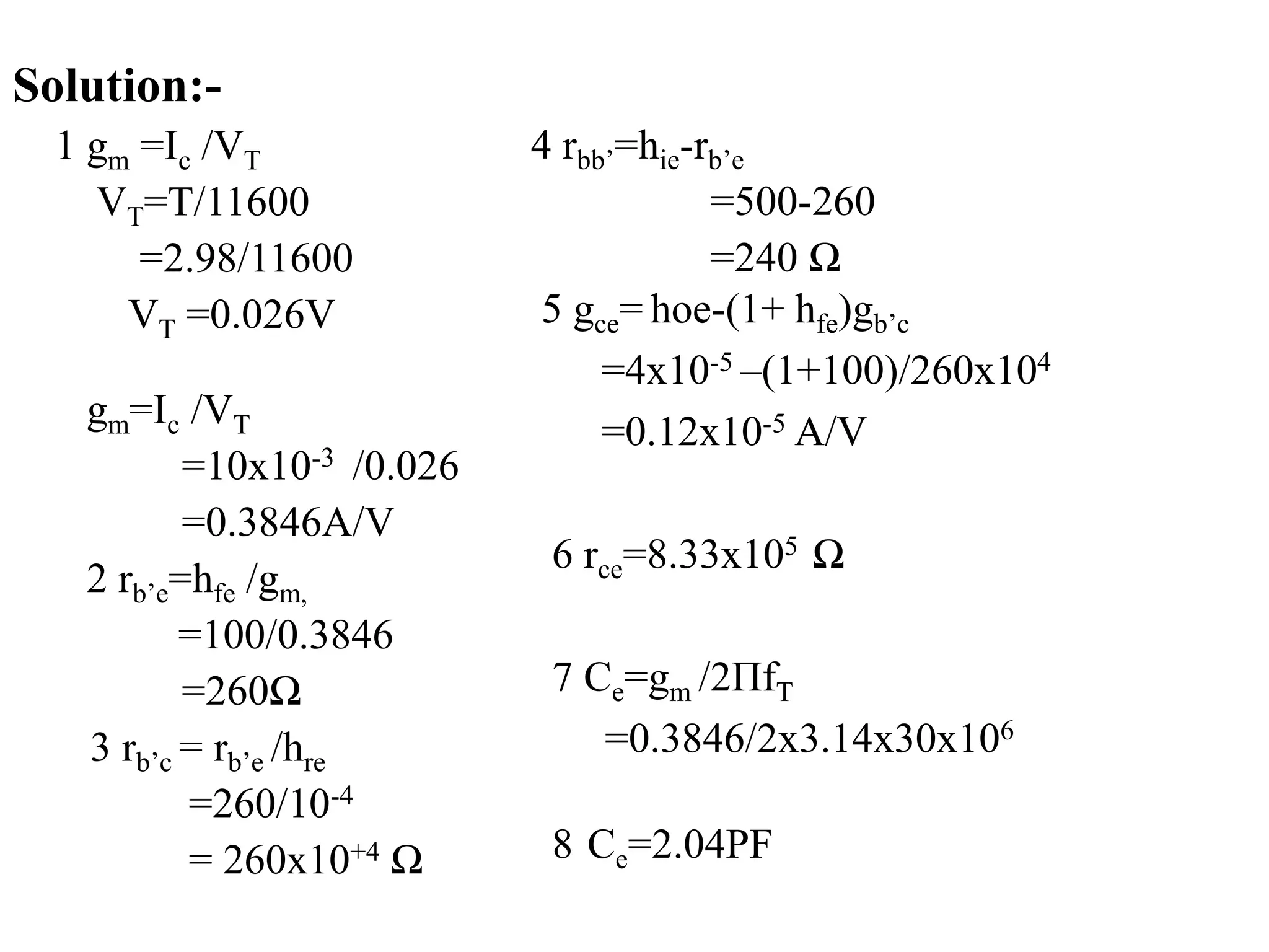
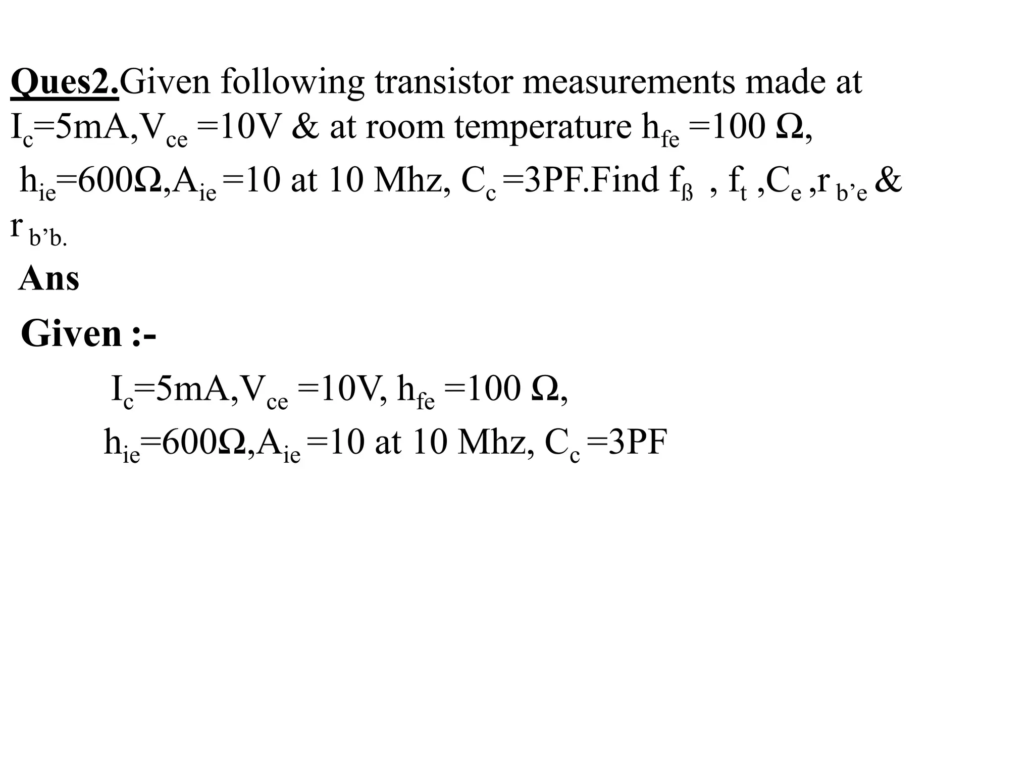
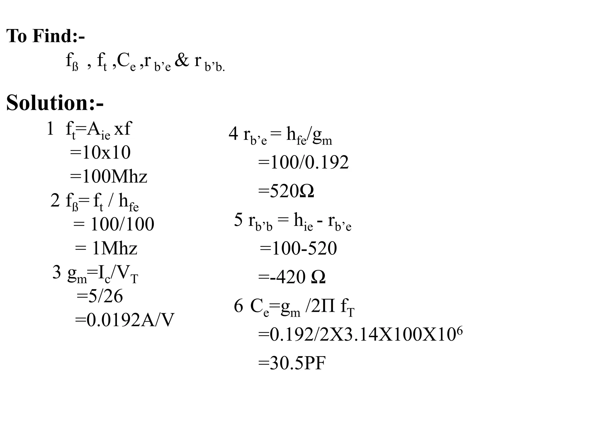
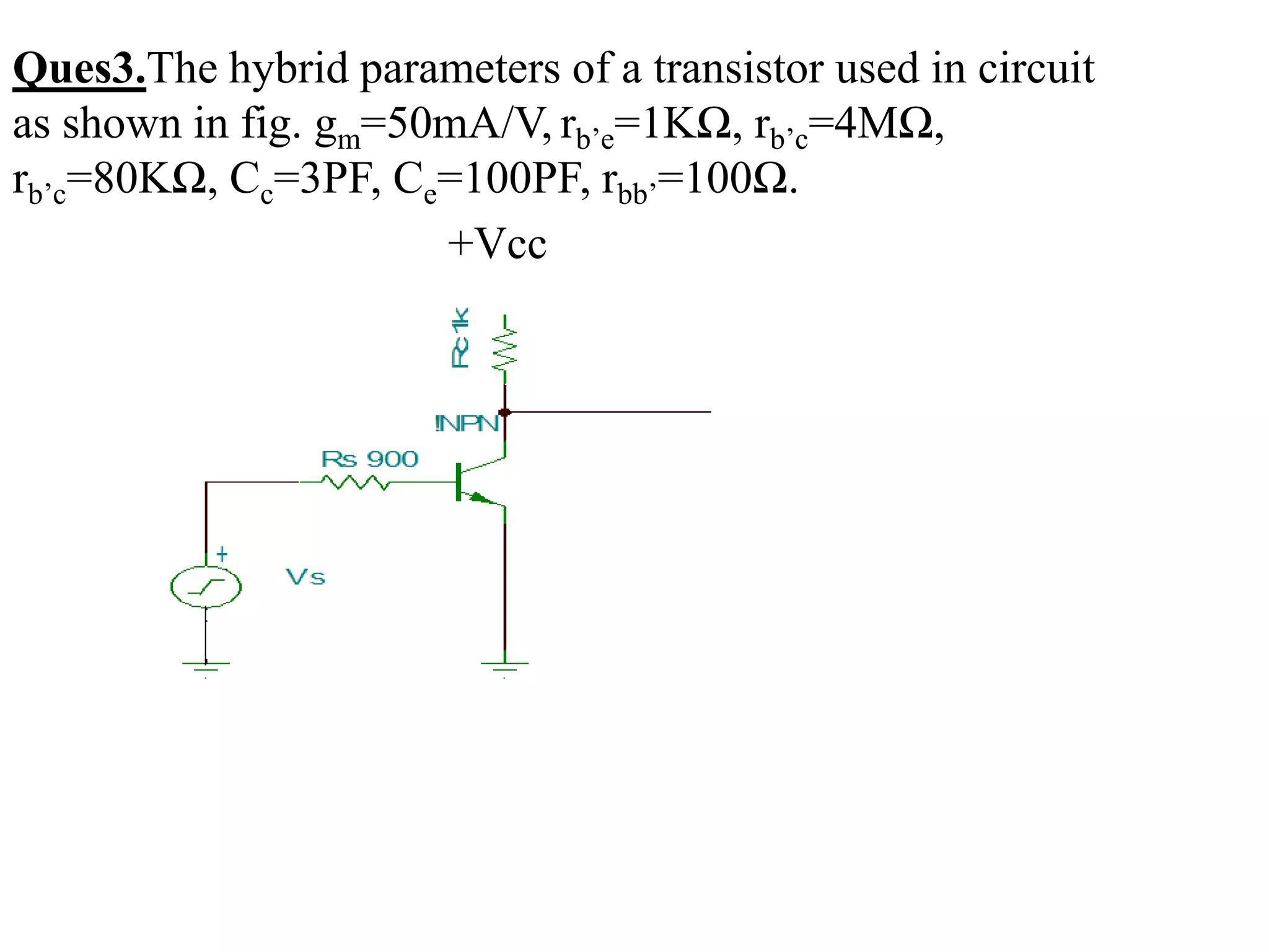
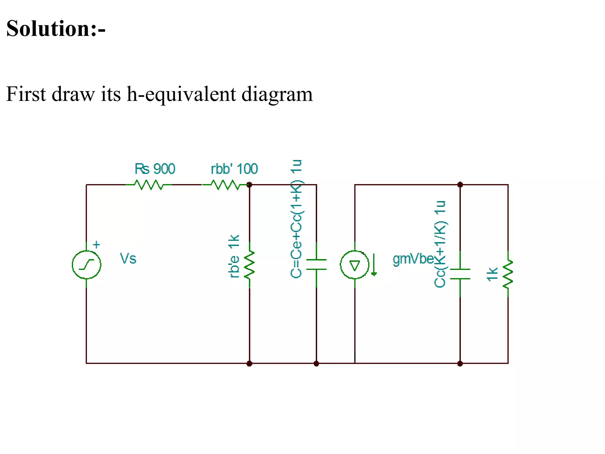
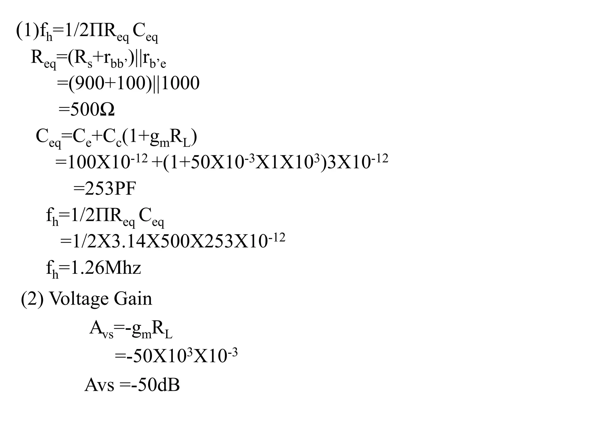
Numerical problems involving hybrid parameters, cutoff frequency, and voltage gains.
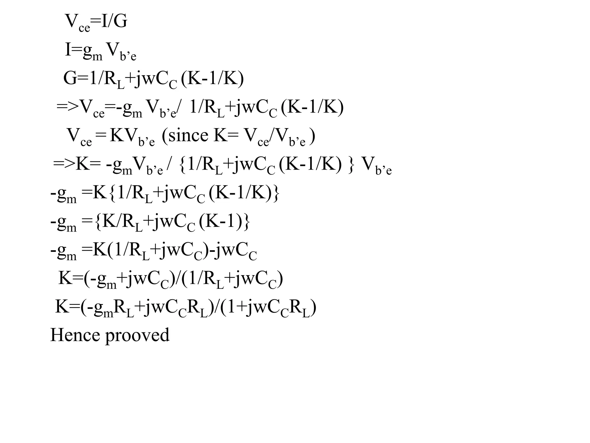
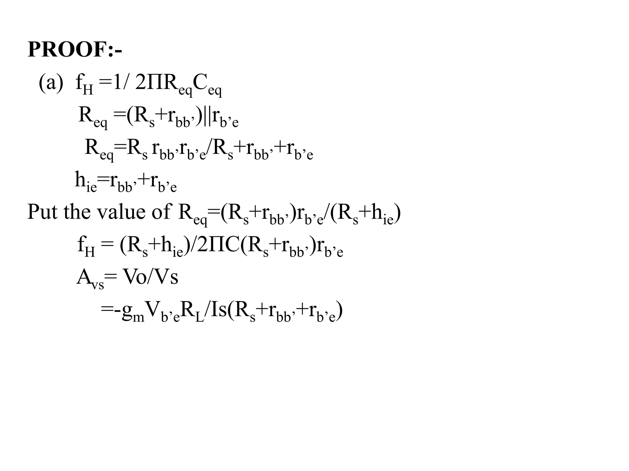
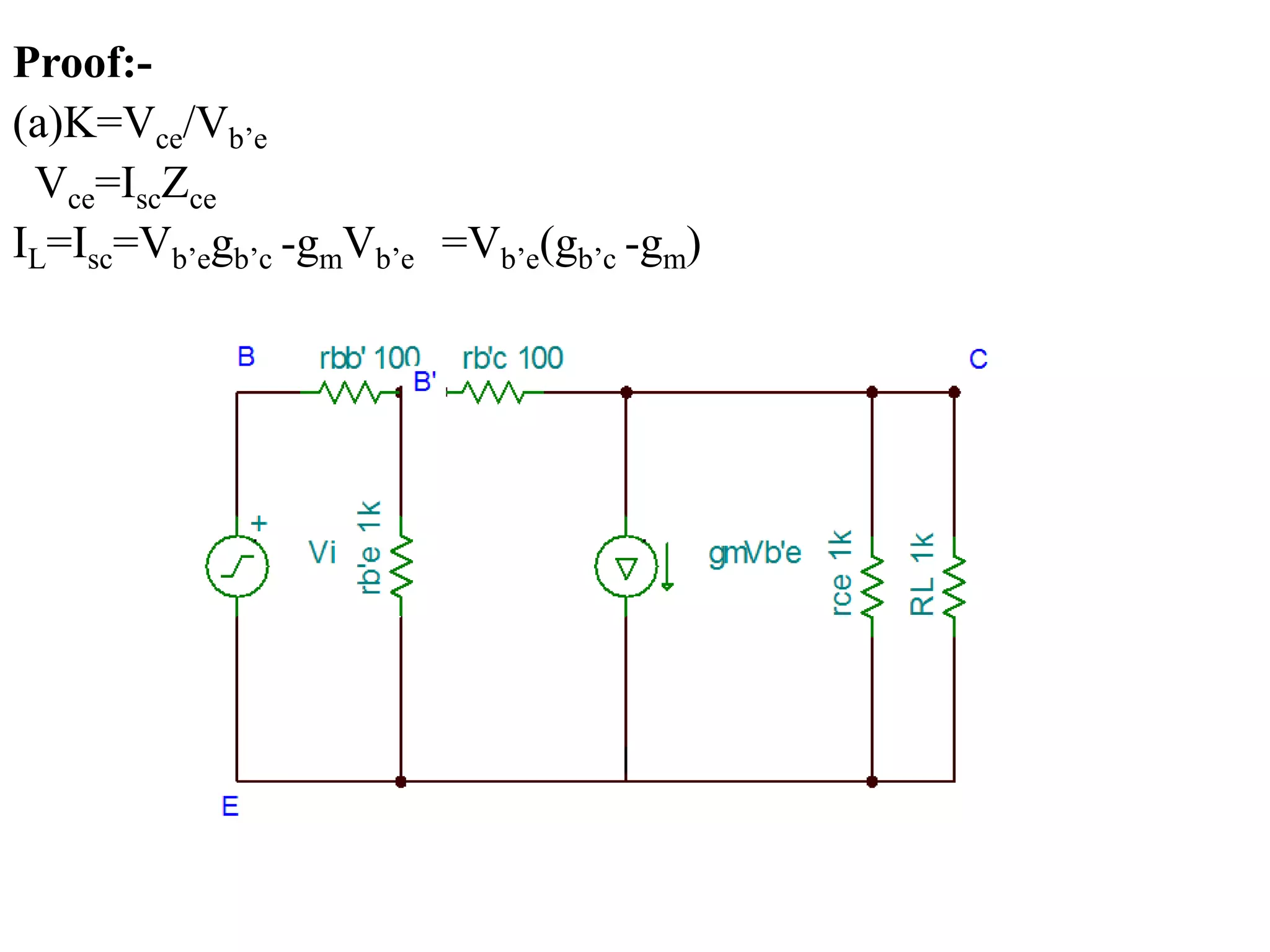
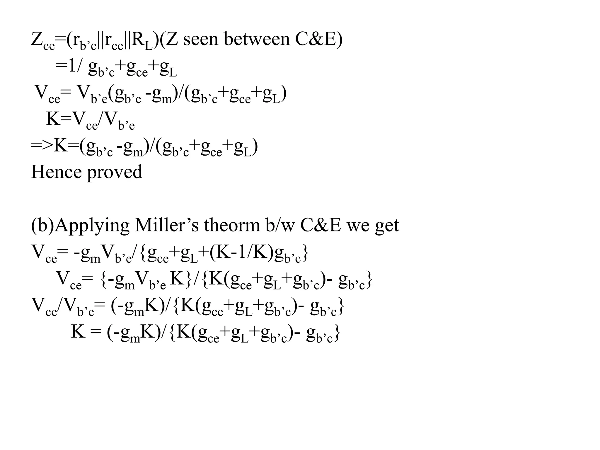
Proofs involving Miller's theorem in relation to hybrid parameters and overall transistor behavior.


![Multisim_simulation_project_3_^0_4[1]-2.pptx](https://cdn.slidesharecdn.com/ss_thumbnails/multisimsimulationproject3041-2-240418183400-1d9cbd89-thumbnail.jpg?width=640&height=640&fit=bounds)


