Compare and contrast the differences between phase-shift, Hartley, Colpitts, and crystal oscillators in terms of frequency stability, amplitude stability, and biomedical applications.
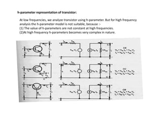
h-parameter representation oftransistor:
At low frequencies, we analyze transistor using h-parameter. But for high frequency
analysis the h-parameter model is not suitable, because :-
(1) The value of h-parameters are not constant at high frequencies.
(2)At high frequency h-parameters becomes very complex in nature.
2.
Common
Emitter
Common
Collector
Common
Base
Definitions
Input Impedance with
OutputShort Circuit
Reverse Voltage Ratio
Input Open Circuit
Forward Current Gain
Output Short Circuit
CE configuration
Vbe= hieIb+hreVce
Ic = hfeIb+hoeVce
CC configuration
Vbc= hicIb+hrcVec
Ie = hfcIb+hocVec
CB configuration
Veb= hibIe+hrbVcb Output Admittance
Input Open Circuit
Veb= hibIe+hrbVcb
Ic = hfbIe+hobVc
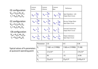
Parameter CE CC CB
hi 1 kΩ or (1100Ω) 1 kΩ or (1100Ω) 21.6Ω
hr 2.5x10⁻⁴ -1 2.9x10⁻⁴
hf 50 -51 -0.98
ho 25µA/V 25µA/V 0.49µA/V
Typical values of h-parameters
at quiescent operating point
3.
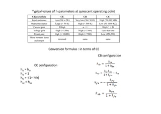
Conversion formulas :in terms of CE
CB configuration
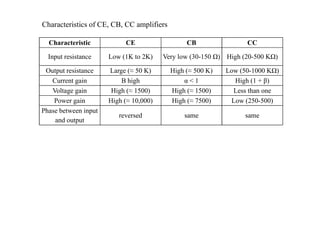
Characteristic CE CB CC
Input resistance Low (1K to 2K) Very low (30-150 Ω) High (20-500 KΩ)
Output resistance Large (≈ 50 K) High (≈ 500 K) Low (50-1000 KΩ)
Current gain B high α < 1 High (1 + β)
Voltage gain High (≈ 1500) High (≈ 1500) Less than one
Power gain High (≈ 10,000) High (≈ 7500) Low (250-500)
Phase between input
and output
reversed same same
Typical values of h-parameters at quiescent operating point
CC configuration
hic = hie
hrc = 1
hfc = -(1+ hfe)
hoc = hoe
CB configuration
4.
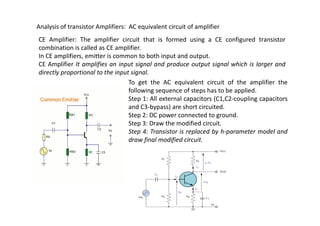
Analysis of transistorAmplifiers: AC equivalent circuit of amplifier
CE Amplifier: The amplifier circuit that is formed using a CE configured transistor
combination is called as CE amplifier.
In CE amplifiers, emitter is common to both input and output.
CE Amplifier It amplifies an input signal and produce output signal which is larger and
directly proportional to the input signal.
To get the AC equivalent circuit of the amplifier the
following sequence of steps has to be applied.
Step 1: All external capacitors (C1,C2-coupling capacitors
and C3-bypass) are short circuited.
Step 2: DC power connected to ground.
Step 2: DC power connected to ground.
Step 3: Draw the modified circuit.
Step 4: Transistor is replaced by h-parameter model and
draw final modified circuit.
5.
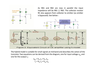
As RB1 andRB2 are now in parallel the input
impedance will be RB1 || RB2. The collector resistor
RC also appears from collector to emitter (as emitter
is bypassed). See below :
The hybrid model is suitable for small signals at mid band and describes the action of the
transistor. Two equations can be derived from the diagram, one for input voltage vbe and
one for the output ic:
vbe = hie ib + hre vce
ic = hfe ib + hoe vce
6.
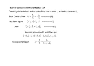
Current Gain orCurrent Amplification (AI):
Current gain is defined as the ratio of the load current I1 to the input current Ib.
Thus Current Gain ------------------- --------------(1)
But from figure
Also
--------------(2)
--------------(3)
Combining Equation (2) and (3) we get,
Combining Equation (2) and (3) we get,
Hence current gain
7.
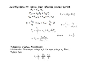
Input Impedance Ri:Ratio of input voltage to the input current
Ri = Vbe / Ib
Where
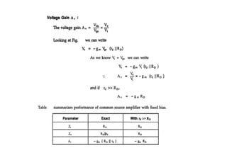
Voltage Gain or Voltage Amplification:
It is the ratio of the output voltage Vc to the input voltage Vb. Thus,
Voltage Gain
8.
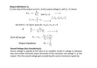
Output Admittance Y0:
Itis the ratio of the output current Ic to the output voltage Vc with Vs = 0. Hence
with VS = 0
But with Vs = 0, Figure gives (Rs + hie) Ib + hre Vc = 0
or
----------2
--------------3
------- 1
(3) In (2) we get
Output impedance
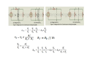
Overall Voltage Gain Considering Rs:
Source voltage Vs applied at the input of an amplifier results in voltage Vb between
bae and emitter terminals (input terminals) of the transistor and voltage Vc at the
output. Then the overall voltage gain considering the source resistance is given by
10.
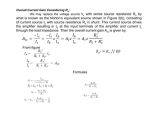
Overall Current GainConsidering Rs:
We may replace the voltage source Vs with series source resistance Rs by
what is known as the Norton’s equivalent source shown in Figure 3(b), consisting
of current source Is with source resistance Rs in shunt. This current source drives
the amplifier resulting in Ib at the input terminals of the amplifier and current IL
through the load impedance. Then the overall current gain AIs is given by:
From figure
Formulas
11.
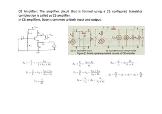
CB Amplifier: Theamplifier circuit that is formed using a CB configured transistor
combination is called as CB amplifier.
In CB amplifiers, Base is common to both input and output.
12.
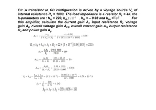
Ex: A transistorin CB configuration is driven by a voltage source Vs of
internal resistance Rs = 1000. The load impedance is a resistor RL = 4k. the
h-parameters are : hib = 220, hrb = , hfb = – 0.98 and h0b = . For
this amplifier, calculate the current gain AI, input resistance Ri, voltage
gain AV, overall voltage gain AVS, overall current gain AIS output resistance
R0 and power gain Ap.
13.
CC Amplifier: Theamplifier circuit that is formed using a CC configured transistor
combination is called as CC amplifier.
In CC amplifiers, Collector is common to both input and output.
14.
Characteristic CE CBCC
Input resistance Low (1K to 2K) Very low (30-150 Ω) High (20-500 KΩ)
Output resistance Large (≈ 50 K) High (≈ 500 K) Low (50-1000 KΩ)
Current gain B high α < 1 High (1 + β)
Voltage gain High (≈ 1500) High (≈ 1500) Less than one
Power gain High (≈ 10,000) High (≈ 7500) Low (250-500)
Phase between input
reversed same same
Characteristics of CE, CB, CC amplifiers
Phase between input
and output
reversed same same
15.
CE amplifier hasa high input impedance and lower output impedance than
CB amplifier. The voltage gain and power gain are also high in CE amplifier
and hence this is mostly used for amplification purpose in AF amplifiers ,RF
amplifiers Signal generators..
Application of CE,CB, CC amplifier
If CC configuration is considered for amplification, though CC amplifier has
better input impedance and lower output impedance than CE amplifier, the
voltage gain of CC is very less which limits its applications to impedance
matching only.
CB amplifier: It is used to match low input impedance source circuit with the
high impedance load. It useful in audio and radio frequency applications as a
current buffer. It is suitable for AF, RF amplifiers as voltage amplifiers.
16.
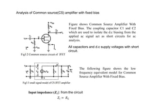
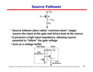
Analysis of Commonsource(CS) amplifier with fixed bias
Figure shows Common Source Amplifier With
Fixed Bias. The coupling capacitor C1 and C2
which are used to isolate the d.c biasing from the
applied ac signal act as short circuits for ac
analysis.
All capacitors and d.c supply voltages with short
circuit.
The following figure shows the low
frequency equivalent model for Common
Source Amplifier With Fixed Bias.
17.
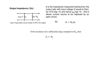
Output Impedance (Zo) :
It is the impedance measured looking from the
output side with input voltage Vi equal to Zero.
As Vi=0,Vgs =0 and hence gmVgs =0 . And it
allows current source to be replaced by an
open circuit.
So
If the resistance rd is sufficiently large compared to RD, then
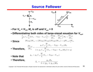
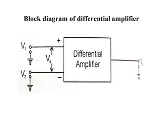
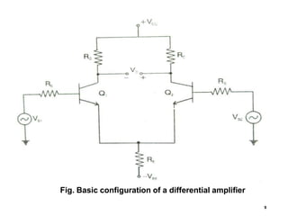
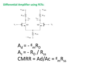
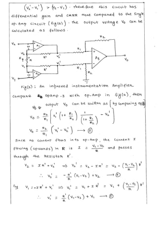
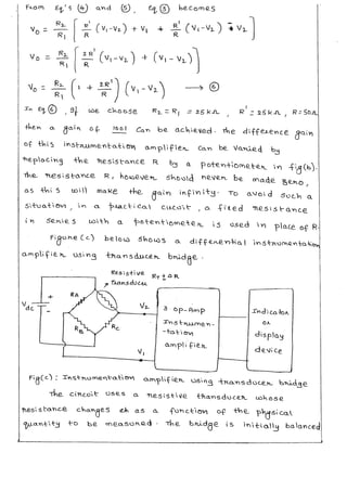
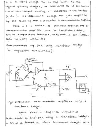
Introduction
• The functionof differential amplifier is to amplify the
difference of two signals.
• The need for differential amplifier in many physical
measurements arises where response from d.c to many
megahertz is required. It is also the basic input stage of an
integrated amplifier.
• The outputsignal in a differential amplifier is proportional to the
difference between the two input signals.
Vo α (V1 – V2)
Where,
V1 & V2 – Two inputsignals
Vo – Single ended output
39.
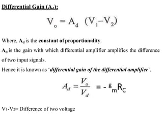
Differential Gain (Ad):
Where,Ad is the constant of proportionality.
Ad is the gain with which differential amplifier amplifies the difference
of two input signals.
Hence it is known as ‘differential gain of the differential amplifier’.
V1-V2= Difference of two voltage
= - g
mRC
40.
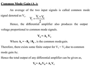
Common Mode Gain(Ad):
An average of the two input signals is called common mode
signal denoted as Vc.
Hence, the differential amplifier also produces the output
voltage proportional to common mode signals.
Vo = Ac Vc
Where Ac = - RC / RE , is the common modegain.
Therefore, there exists some finite output for V1 = V2 due to common
mode gainAc.
Hence the total output of any differential amplifier can be given as,
Vo= Ad Vd + AcVc
41.
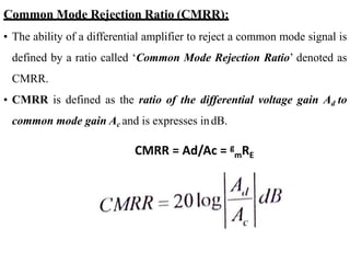
Common Mode RejectionRatio (CMRR):
• The ability of a differential amplifier to reject a common mode signal is
defined by a ratio called ‘Common Mode Rejection Ratio’ denoted as
CMRR.
• CMRR is defined as the ratio of the differential voltage gain Ad to
common mode gain Ac and is expresses indB.
CMRR = Ad/Ac = g
mRE
42.
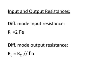
Input and OutputResistances:
Diff. mode input resistance:
Ri =2 re
Diff. mode output resistance:
Ro = RC // ro
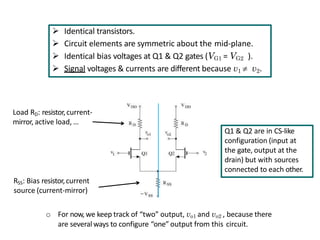
Identical transistors.
Circuit elements are symmetric about the mid-plane.
Identical bias voltages at Q1 & Q2 gates (VG1 = VG2 ).
Signal voltages & currents are different because v1 v2.
Load RD: resistor,current-
mirror, active load, …
RSS: Bias resistor,current
source (current-mirror)
o For now, we keep track of “two” output, vo1 and vo2 , because there
are several ways to configure “one” output from this circuit.
Q1 & Q2 are in CS-like
configuration (input at
the gate, output at the
drain) but with sources
connected to each other.
45.
ID ID
ID
ID
2ID
VGS1 VGS 2 VGS
VOV 1 VOV 2 VOV
ID 1 ID 2 ID
VDS1 VDS 2 VDS
S
S1 S2
and V V V
Since VG1 VG 2 VG
gm1 gm 2 gm
ro1 ro 2 ro
Also:
46.
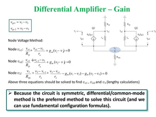
Differential Amplifier –Gain
v3
r
R
g (v v ) 0
R r
gm (v1 v3) gm (v2 v3) 0
v3 vo 2 v3 vo1
SS
R ro ro
m 2 3
g (v v ) 0
o
vo 2 v3
D
m 1 3
D o
vo1 vo1 v3
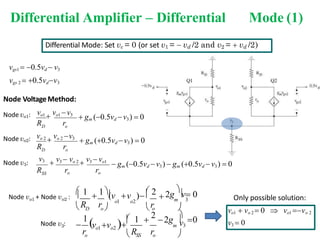
Node Voltage Method:
Node vo1:
Node vo2: vo2
Node v3:
Above three equations should be solved to find vo1 , vo2 and v3 (lengthy calculations)
vgs1 v1 v3
vgs 2 v2 v3
Because the circuit is symmetric, differential/common-mode
method is the preferred method to solve this circuit (and we
can use fundamental configuration formulas).
47.
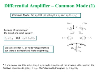
Differential Amplifier –Common Mode (1)
Because of summery of
the circuit and input signals*:
Common Mode: Set vd = 0 (or set v1 = vc and v2 = vc )
vo1 vo 2 and id1 id 2 id
We can solve for vo1 by node voltage method
but there is a simpler and more elegant way.
id
id
id
2id
* If you do not see this, set v1 = v2 = vc in node equations of the previous slide, subtract the
first two equations to get vo1 = vo2 . Ohm’s law on RD then gives id1 = id2 =id
48.
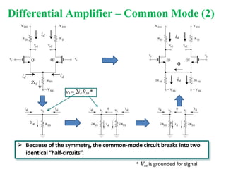
Differential Amplifier –Common Mode (2)
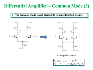
Because of the symmetry, the common-mode circuit breaks into two
identical “half-circuits”.
id
id
id
2id
id
0
id
v3 2id RSS *
* Vss is grounded for signal
Differential Amplifier –Differential Mode (1)
R
v3
r
R
R r
gm (0.5vd v3) gm (0.5vd v3) 0
ro ro
v3 vo 2 v3 vo1
SS
gm (0.5vd v3) 0
o
D
vo 2 vo 2 v3
gm (0.5vd v3) 0
D o
vo1 vo1 v3
vgs1 0.5vd v3
vgs 2 0.5vdv3
Node VoltageMethod:
Node vo1:
Node vo2:
Node v3:
Differential Mode: Set vc = 0 (or set v1 = vd /2 and v2 = vd /2)
r
1 1
o
o1 o2
(v v )
R r
D o
2
2g
v 0
m 3
1
1
r
2 2g
0
m v3
R r
SS o
vo1 vo2
o
o1 o2
Node v + Node v :
3
Node v :
vo1 vo 2 0 vo1 vo 2
v3 0
Only possible solution:
51.
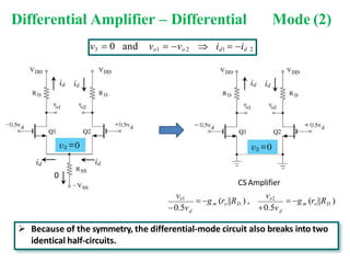
Differential Amplifier –Differential Mode (2)
Because of the symmetry, the differential-mode circuit also breaks into two
identical half-circuits.
v3 0 and vo1 vo 2 id1 id 2
v3 =0
id id
v3 =0
CS Amplifier
d d
vo2
vo1
gm o D
(r ||R )
0.5v
gm o D
(r ||R ) ,
0.5v
id
id
0
id id