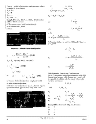
SlideShare a Scribd company logo
1 of 11
Download to read offline
30 4A.273
© Copy Right: Rai University
ELECTRONICDESIGNTECHNOLOGY
Objective :
To understand the Hybrid Equivalent model of Transistor.
Hello! Students I hope now you are well versed with the
concepts of transistor re
-model and the different configuration
that we have studied in the last lectures. Now in today’s class we
are going to discuss the hybrid-model for the various configura-
tion.
To analyze the behavior of transistor amplifier with the help of
β and the values of resistances used in the circuit, is not so
accurate. It is because the input and output circuits of the
amplifier are considered to be completely independent and
some of the effects are ignored such as IC
is taken as constant
but actually its value depends upon load resistance.
Therefore, more accurate method to analyze a transistor
amplifier is hybrid parameters (h- parameters) method, we can
study h-parameter at low frequency and at high frequency. So
this chapter first introduces h- parameter at low frequency and at
high frequency. So this chapter first introduces h – parameter at
low frequency and after that hybrid-π model (for high fre-
quency).
Hybrid Parameters (For Low Frequency)
The four * parameters which are used to analyze any linear
circuit having input and output terminals are called hybrid or
h-parameters.
Meaning of hybrid is ‘mixed’. Since these parameters have
mixed dimensions, they are called hybrid-parameters.
Determination of h-parameters
Consider a linear circuit having two input and two output
terminals (See Fig. 2.29). Their input and output voltage and
currents are labeled with their positive directions. The conven-
tions used are the standard one which may not correspond to
the actual directions. However, while analyzing the circuit, if any
direction is opposite that may be considered as negative.
LINEAR CIRCUIT
Fig. 2.29
In Fig. 4.1, the voltages and currents can be related by the
following set of equations:
v1
= h11
i1
+ h12
v2
.
…(i)
i2
= h21
i1
+ h22
v2
.
…(ii)
Where h11
, h21
, h12
and h22
are fixed constants and are known as
hybrid-parameters. These parameters relate the four variables i.e.
i1,
i2
, v1
and v2
by the above-said two equations.
If we look at the equation. (i), it is clear that h11
has the dimen-
sion of ohm whereas h12
, has no dimension. Similarly, if we
look at the eqn.. (ii), h2l
has no dimension but h22
, has the
dimension of mho. Hence, the four parameters are named as
hybrid (having mixed dimensions) parameters.
These parameters can be determined very easily as explained
below:
(i) Short-circuit the output terminals, as shown in Fig. 2.30(a),
the output voltage reduces to zero i.e. v2
, = 0. Substituting
this value in eqns. (i) and (ii). we get
v1
= h11
+ h12 × 0
Fig. 2.30 (a) and (b)
or h11 =
1
1
t
v
(output short circuited; v2 = 0) ….(iii)
and t2 = h21 i1 + h22
× 0
or h21 =
1
2
i
i
(output short circuited; v2 = 0) ….(iv)
Here, h11
is called input impedance (i.e. v1
/ ii
) with output
shorted and h2l
is called current gain (i.e. i2
./ i1
) with output
shorted.
(ii) Open circuit the input terminals, as shown in Fig. 2.30b, the
input current reduces to zero i.e. i1
= 0. Substituting this
value in eqns. (i) and (ii), we get,
v1 = h11× 0 + h12 v2
or h12 =
2
1
v
v
(input opened; i1 = 0) ….(v)
and i2 = h21
×
0 + h22 v2
or h22 =
2
2
v
i
(input opened; i1 = 0) ….(vi)
Here, h12
is called voltage feedback ratio (i.e. v1
/v2
) with input
terminals open and h2
is called output admittance (i.e.i2
/ v2
)
with input terminal open.
LESSON 8:
(HYBRID EQUIVALENT MODEL)
UNIT - 2
(SMALL SIGNAL ANALYSIS FOR BJT :
SINGLE STAGE AND MULTISTAGE
AMPLIFIER)
© Copy Right: Rai University
4A.273 31
ELECTRONICDESIGNTECHNOLOGY
Hybrid-Parameter Equivalent Circuit
Fig. 2.31 &2.32
A two port linear circuit is shown in Fig. 2.31. The voltages and
currents of the circuit can be expressed in terms of h-parameters
by the expressions;
V1= h11 i1 + h12 v2
...(i)
i,2 = h21 i1 + h22 v2
...(ii)
The h-parameters’ equivalent circuit is shown in Fig. 2.32. The
input circuit (or port) is derived from the exp. (i). Here, input
impedance (resistor) h is connected in series with a voltage
generator h12
v2
. The output circuit (or port) is derived from exp.
(ii) it involves current generator h2l
v2.
and shunt resistor h22
.
Example.1 Determine the h-parameters of the circuit
shown in Fig. 2.33.
Fig. 2.33 & 2.34
Solution. To determine h- parameters of the circuit proceed as
follows:
(i) Short-circuit the output terminals as shown in fig 2.34 can
determine h11
and h21
.
Since 10 Ω resistor is short circuited
h11
= 2 Ω
Now, current i1
flows into the box and the same current flows
out of the box.
∴ i2
= i1
.
And h21 = 1
1
1
1
2
−=
−
=
i
i
i
i
(ii) Open the input terminals and make the arrangement as
shown in Fig. 2.35. It may be noted that output terminals
are driven by voltage v2
and no current flows through 20
Ωresistor. Hence, the voltage across 10 Ω resistor i.e. v2
reaches across the input terminals.
∴ v1
= v2
Figure 2.36
and 1
2
2
2
1
==
v
v
v
v
Output impedance = 10 Ω
∴ Output impedance,
h22
= 01.0
10
1
mh=
Hence the various h-parameters of the circuit are
h11
= 20 Ω; h21
= -1
h12
= 1; h12
= 0.1 mho
Example.2 To determine the h-parameter of the circuit shown
in Fig 2.36
Solution. To determine h- parameters of the circuit proceed as
follows:
(i) Short circuit the output terminals as shown in Fig. 4.10.
h11 = 6 + 8 | | 8 = 6 + =
+
×
88
88
10Ω
Now, the input current i1
is divided equally at the junction.
Fig.2.36
∴ i2 = 1
1
5.0
2
i
i
−=−
h21 = 5.0
5.0
1
1
1
2
−=−=−
i
i
i
i
32 4A.273
© Copy Right: Rai University
ELECTRONICDESIGNTECHNOLOGY
Fig.2.37&2.38
(ii) Open the input terminals and make the arrangement as
shown in Fig. 2.38. Here, no current flows through 6 il
resistor as the output terminals are driven by voltage v2
.
v1 = 2
22
5.08
16
8
88
v
vv
=×=×
+
∴ h12 = 5.0
5.0
2
1
2
2
==
v
v
v
v
Impedance looking into the output terminals = 8 + 8 = 16 Ω
h22 =
16
1
= 0.0625 mho
Hence, the various h-parameters of the circuit are
h11
. = 10 Ω ; h21
= - 0.5 ; h12
= 0.5 ; h22
= 0.0625 mho
Performance of a Linear Circuit In
H- Parameters
It has already been seen that a linear circuit has a set of h-
parameters. Now, we shall study the performance of such a
circuit by developing expressions for input impedance, current
gain, voltage gain etc. in terms of h-parameters.
Figure 2.40
Consider a circuit having load resistance RL
across its output
terminal as shown in Fig. 2.39.
Input Impedance
The ratio of input voltage to input current is called the input
impedance Zin
.
∴ Zin.=
i
i
i
v
or Zin.=
1
212111
i
vhih +
(∴ v1= h11 i1 + h12 v2)
or Zin. = h11 +
1
212
i
vh
….(i)
Now, i2 = h21 i1 + h22 v2
or 






 −
=∴+=
−
LL i
v
ivhih
i
v 2*
2222121
2
or -h21 i1 = v2 = 





+
L
r
h
1
22
The ratio of output current to input current is called current
gain Ai
.
Zin = h11 -
Lr
h
hh
1
22
2112
+
…..(iii)
We know, i2
= h21
i1
+ h22
v2
and v2
= -i2
RL
.
(from output circuit)
i2
= h21
i1
+ h22
(-i2
RL
)
i2
= h21
i1
+ h22
rL
i2
.
or i2 (1 + h22 RL) = h21 i1.
or
Lrh
h
i
i
22
21
1
2
1+
=
Substituting the value of
1
2
i
i
in eqn.(iv), we get,
A1
=
Lrh
h
22
21
1+
…..(v)
If h22
rL
<< 1 then Ai ≅ h21
.
Voltage Gain
The ratio of output to input voltage is called voltage gain Av
.
Av
=
1
2
v
v
……(vi)
or Av
=
in
zi
v
1
2
( )11 inZiv =Θ
© Copy Right: Rai University
4A.273 33
ELECTRONICDESIGNTECHNOLOGY
Substituting the value of
1
2
i
v
from eqn. (ii), we get,
Av
=
in
L
Z
r
h
h






+
−
1
22
21
H- Parameters of a Transistor
A transistor in a three–terminal device. If any one of the
terminals is made common to the input and output, it will
have two ports. Thus it will have two input terminals and two
output terminals (See Fig.2.40), for a small ac signal transistor
behave as a linear device, hence it can be described in terms of h-
parameters.
The voltages and currents of the circuit can be related by the
following sets of equations:
Figure 2.40
V1
= h11
i1
+ h12
v2
….(i)
i2
= h21
i1
+ h22
v2
….(ii)
where the various h-parameters are;
h11
=
1
1
i
v
02=v = Input impedance (with
output shorted) = hi
(in ohms)
h21
= 02
1
2
=v
i
i
= Forward current ratio (with
output shorted) = hf
(no unit)
h12
= 01
2
1
=i
v
v
= Reverse voltage ratio (with
input open)= hr
(no unit)
h22
= 01
2
2
=i
v
i
= Output admittance (with
input open=* h0
(in mho)
While considering the behaviour of ransistor in terms of h-
parameters, the following points need attention:
i) The value of h-parameters of transistor will depand upon the
transistor connection (i.e. CE, CB or CC). Therefore. h-
parameters for different connections are abbreviated in
different way. For instance, h11
is represented as **hie
, hib
and
hic
for CE, CB and CC connections.
ii) While checking the performance, ac output resistance is
considered as load resistance i.e.
LC
LC
LCACL
RR
RR
RRRr
+
===
The values of h-parameters depend upon the Q point. If Q
point changes, the values of h-parameters are also changed.
In transistor circuits the values of voltage and currents are taken
depending upon transistor configuration. For example, for CE
configuration
cce
bbe
IiVv
IiVv
==
==
22
11
;
;
where Vbe, Ib, Vce and Ic are the rms values.
The nomenclature used for the h-parameters of a transistor
depending upon its connections is given in the following table
4.1.
Table 2.1
S.No. h-parameters
CE
Configuration
CB
Configuration
CC
Configuration
1 h11 hie hib hie
2 h12 hre hrb hrc
3 h21 hfe hfb hfc
4 h22 h0e h0b h0c
The typical values of h-parameters of a 2N 3904 transistor are
given below:
hie = 3.5 k Ω; hre =1.3 x 10⁻⁴
hfe = 120; hoe = 8.5 µ mho
*It may be noticed that subscript used is the first letter of the
description i.e. input, forward, reverse and output respectively.
** It may be noticed that the second letter of the subscript used
indicates the type of transistor connections.
Performance of (Ce Circuit) Transistor in
H-Parameters
While studying the performance of a transistor, we are inter-
ested in the following terms:
i) Input Impedance
The general expression for Zin is
L
in
r
h
hh
hZ
1
22
2112
11
+
−=
Substituting the values of h-parameters for transistor in CE
configuration. We get,
34 4A.273
© Copy Right: Rai University
ELECTRONICDESIGNTECHNOLOGY
L
e
fere
iein
r
h
hh
hZ
1
0 +
−=
(ii) Current gain
The general expression is
L
i
rh
h
A
22
21
1+
=
Substituting the values of h-parameters for transistor in CE
configuration, we get,
Le
fe
i
rh
n
A
01+
=
(iii) Voltage gain
The general expression is
in
L
v
Z
r
h
h
A






+
−
=
1
22
21
Substituting the values of h-parameters for transistor in CE
configuration, we get,
in
L
e
fe
v
Z
r
h
h
A






+
−
=
1
0
The expressions for Zin Ai and Av for other transistor connec-
tions (i.e.CB and CC) can be obtained similarly.
Example.3 An amplifier circuit is shown in Fig. 2.41. Work out
the following quantities for the circuit:
i) ac emitter current
ii) ac voltage at emitter, based and collector
iii) voltage gain.
Assume hie
or rin
=250 W
Figure 2.41
Solution. (i) Base current due to signal
ib =
)(20
250
5
valuepeakA
mV
r
v
in
in
µ=
Ω
=
Collection current due to signal (peak value)
mAAAii bc 110002050 ==×== µµβ
Emitter current due to signal (peak value)
mAmAAiii bce 102.11020201000 ≅==+=+= µ
(ii) ac voltage at emitter,
0=ev (since it is connected to earth
through CE
)
)(5 peakmVvb =
VkmARiRiv ccACcc 111 =Ω×=×==
(iv) Voltage gain, Av
= .200
5
1
===
mV
V
v
v
v
v
in
c
in
out
Example.4 A single stage amplifier circuit using transistor AC
126 is shown in Fig. 2.42. Draw its ac equivalent circuit and
calculate the voltage gain with an without RL
. Assume the
following transistor parameters:
Ω== krorhorh inieacfe 5.1;150β
Figure 2.42
© Copy Right: Rai University
4A.273 35
ELECTRONICDESIGNTECHNOLOGY
Solution. To draw the ac equivalent circuit of an amplifier the
dc voltages and capacitors are short circuited. Thus, the resultant
ac equivalent circuit is shown in Fig. 2.43.
Let the ac base current due to signal be 10 mA,i.e.
andAib µ10=
signal voltage, mVkAriv inbin 155.110 =Ω×=×= µ
Collector current,
mAAii bc 5.1150010150 ==×=×= µβ
Output voltage, Lcout riv ×=
(i) When load resistance RL
is considered
rL
= RAC
= RC
|| RL
= Ω=
+
×
k5.0
11
11
VkmAvout 75.05.05.1 =Ω×=∴
Voltage gain, 50
1015
75.0
15
75.0
3
=
×
=== −
mV
V
v
v
A
in
out
v
(ii) When load resistance RL
is not considered
rL
= RC
= 1kW
VkmAvout 5.115.1 =Ω×=∴
Voltage gain, .100
15
5.1
===
mV
V
v
v
A
in
out
v
Example. 5 A CE amplifier has the following h-parameters:
4
105.2,1100 −
×== reie hohmh
mhomicrohh oefe 25,50 ==
If the load and source resistance both are 1 Kilo-ohm, find
current and voltage gain.
Solution: Here Rs
=1kW and rL =
1kW= Ω× 3
101
Current gain, Ai =
Loe
fe
Rh
h
×+1
36
10110251
50
×××+
= − = 78.48
025.01
50
=
+
Voltage gain,
inoe
fe
v
Z
rL
h
h
A






+
−
=
1
Where Zin
=
36
4
1011025
50105.2
1100
1 −−
−
×+×
××
−=
+
−
L
oe
fere
ie
r
h
hh
h
=100-12.5=1087.5W
977.45
5.1087)1011025(
50
36
−=
××+×
−
=∴ −−vA
The negative sign shows that the output voltage is 1800
out of
phase to the input signal.
Example.6. A transistor amplifier circuit is shown in Fig. 4.17.
The h-parameters of the transistor are as under.
hie
= 1500W ; hfe
= 100
hre
=4 mhohoe
44
104;10 −−
×=×
Determine the ac input impedance of the amplifier and the voltage gain.
Figure 2.44
36 4A.273
© Copy Right: Rai University
ELECTRONICDESIGNTECHNOLOGY
Solution. At load resistance of the amplifier,
rL
= Ω=Ω=
+
×
= 80008
4010
4010
kRAC
Input impedance, Zin
=
L
oe
fere
ie
r
h
hh
h
1
+
−
=
Ω=
+×
××
−
−
−
1424
8000
1
104
100104
1500
4
4
AC input resistance of the entire stage *(Rac
)
= Zin
| | R1
| | R2
=1424 | |
100 Ω=×× 1366100050||1000
Voltage gain, Av
=
134
1424
8000
1
104
100
1 4
−=






+×
−
=






+
−
−
in
L
oe
fe
Z
r
h
h
The magnitude of gain is 134 but the output is 1800
out of
phase to the input signal.
Experimental Determination of
Transistor H-parameters
For the determination of transistor h-parameters, consider the
circuit shown in Fig. 2.45. The standard equations for linear
circuit are
2121111 vhihv +=
2221212 vhihi +=
Taking rms values of voltages and currents and using standard
transistor nomenclature, the above equations cab ne written as
cerebiebe VhihV += … (i)
cecebfec VhihI += ….(ii)
Determination of hfe
and hie
Short circuit the output as showing in Fig. 2.46. This is
accomplished by making the capacitor C2
deliberately of large
value so that it can carry the short circuit current.
This makes *Vce
= 0
Fig.2.45
*Vce
= 0 means only ac output is zero. It does not effect the dc
collection to emitter voltage VCE
Substituting this value in equa. (i) and (ii), we get,
0×+= rebiebe hIhV
or
b
be
ie
I
V
h = ….(iii)
0×+= oebfec hIhI
or
b
c
fe
I
I
h = …..(iv)
Determination of hre
and hoe
Open circuit the input ( no signal is applied) as shown in Fig.
4.20 but a signal generator is applied across the output. Measure
Vbe,
Vce
and Ic.
. The large reactance connected in the base circuit
does not allow the ac current to enter base resistor RB
. At the
same time reactor has a low resistance so that may not affect the
operating point. Under this condition Ib
=0
© Copy Right: Rai University
4A.273 37
ELECTRONICDESIGNTECHNOLOGY
Substituting this value in eqns. (i) and (ii), we get,
cereiebe VhhV ×+×= 0
or
ce
be
re
V
V
h = …(v)
ceoefec VhhI ×+×= 0
or
ce
c
oe
V
I
h = ….(vi)
Figure 2.47
Example.7 In a CE amplifier circuit, the following quantities
are measured:
i) When ac output is short circuited (i.e Vce
=0)
mVVmAIAI becb 15;5.1;15 === µ
ii) When ac input is opened (i.e., Ib
=0)
VVAImVV cecbe 5.1;90;1 === µ
Determine all the h-parameters of the circuit. Assuming that all
the values are ac rms.
Solution. The various h-parameters are calculated as under:
Ω=== 1000
15
15
A
mV
I
V
h
b
be
ie
µ
Ω=== 100
5.1
5.1
A
mV
I
I
h
b
c
fe
µ
3
1066.0
5.1
1 −
×===
A
mV
I
V
h
b
be
re
µ
mho
V
A
V
I
h
ce
c
oe µ
µ
60
15
90
===
Approximate Analysis
For a typical transistor RC
= 1K and hoe
=25mS
CC
oe
oe
RR
h
K
h
≈
=
||
1
40
1
Θ
hence
∴ hoe
may be neglected.
Also , hre
=2.5 4
10−
×
Figure 2.49a Common Emitter Configuration
Θ feedback voltage hre
vc
is very small and can be omitted.
Therefore, hybrid ac equivalent circuit becomes. Thus , the
comparison for hybrid versus re
model for (a) common emitter
and (b) common base configuration can be given, as shown in
fig. 4.33
Figure 2.50 Common Base Configuration
38 4A.273
© Copy Right: Rai University
ELECTRONICDESIGNTECHNOLOGY
Thus, the re
model can be converted to a hybrid model and vice-
versa using the given relations
rehie β=
β=feh
rehib =
1−≅−= αfbh
Example.9: Given IE
= 2.5mA, hfe
=140, hoe
=20 mS (mmho)
and hob =0.5mS, determine:
a) The common-emitter hybrid equivalent circuit.
b)The common-base re
model.
Solution:
Figure 2.51 Common Emitter Configuration
(a) Ω=== 4.10
5.2
2626
mA
mV
I
mV
r
E
e
Ω=Ω== kh reie 456.1)4.10)(140(β
Ω=== k
Sh
r
oe
o 50
20
11
µ
(b) Ω===≅
Ω=
M
Sh
r
r
ob
o
e
2
5.0
11
1
4.10
µ
α
(a) Common-Emitter Configurations using hybrid model.
(i) Fixed bias configuration
For the fixed bias configuration of fig.2.53 a, the small signal ac
equivalent model will appear as shown in Fig. 2.53b. Here,
Zi
: ZI
= RB
||hie
Zo
: Zo
=RC
||1/hoe
Av
: Using R=1/hoe
||RC
''00 RIhRIV bfe−=−=
and
ie
i
b
h
V
I =
with '0 R
h
V
hV
ie
i
fe−=
so that
ie
oeCfe
i
V
h
hRh
V
V
A
)/1||(0
−==
AI
: Assuming that RB
>>hie
and 1/hoe
³10R,
then Ib
@Ii and Io
=
Ic
= hfe
Ii
with
fe
i
o
h
I
I
Ai ≅=
Av
:
ie
oeCfe
h
hRh
Av
)/1||(
−=
Ai:
ie
fe
hR
Rh
Ai
+
=
'
'
(ii) Unbypassed Emitter-Bias Configuration.
For the CE unbypassed emitter-bias configuration of Fig. 2.54
the small-signal ac model will be the same as re - model , with
bre
replaced by hie
and bIb
by hfe
Ib
. The analysis will proceed in
exactly the same manner.
Zi
: Zb
@ hfe
RE
and ZI
= RB
||Zb
Zo
: Zo
=RC
Av
:
Efe
Cfe
b
Cfe
v
Rh
Rh
Z
Rh
A −≅−=
and Av
@
E
C
R
R−
AI
:
bB
Bfe
i
ZR
Rh
A
+
=
Example.10 For the network of Fig. 2.55, determine:
(a) Zi
.
(b) Zo
.
(c) Av
.
(d) Ai
.
© Copy Right: Rai University
4A.273 39
ELECTRONICDESIGNTECHNOLOGY
Solution:
Figure 2.55
(a) ZI
= RB
||hie
= 330kW||1.175 kW @ hie
=1.171kW
(b) Ω=== k
VAh
r
oe
o 50
/20
11
µ
CC
oe
o RkkkR
h
Z ≅Ω=ΩΩ== 56.27.2||50||
1
(c)
34.262
171.1
)50||7.2)(120()/1||(
−=
Ω
ΩΩ
−=−=
k
kk
h
hRh
A
ie
oeCfe
v
(d) 120=≅ fei hA
(iii) Voltage-divider Configuratioin
For the voltage-divider bias configuration of Fig. 2.56 the
resulting small-signal ac equivalent network will have the same
appearance as Fig. 2.53b with RB
replaced by R’=R1
||R2
ZI
: From Fig. 2.54 with RB
=R’
ZI
=R’|| hie
Zo
: From Fig. 2.54,
Co RZ ≅
Fig. 2.56
or
C
i
R
Z
AvA 1
−=
(b) Emitter-Follower configuration
For the emitter-follower of fig. 2.57a the small –signal ac model
will match Fig. of re model bre
= hie
and b = hfe
The resulting equations will therefore be quite similar.
Zi
:
Zb
@ hfe
RE
Zi
=RB
||Zb
Fig. 2.57a Emitter-follower configuration.
Fig. 2.57b Defining Zo for the emitter-follower configura-
tion.
Zo
:
For Zo,
the output network defined by the resulting equations
will appear as shown in Fig. 4.32.
Zo
=RE
||
fe
ie
h
h
+1
or since 1+ fefe hh ≅
Zo
= RE
||
fe
ie
h
h
40 4A.273
© Copy Right: Rai University
ELECTRONICDESIGNTECHNOLOGY
Av
: For the voltage gain the voltage-divider rule can be applied
to Fig. 2.57a as follows
)1/(
)(
feieE
iE
o
hhR
VR
V
++
=
since 1+hfe
@hfe’
feieE
E
i
o
v
hhR
R
V
V
A
/+
≅=
Ai:
bB
Bfe
i
ZR
Rh
A
+
=
or Ai
= -Av
E
i
R
Z
Fig. 2.57a Emitter-follower configuration.
Fig. 2.57b Defining Zo for the emitter-follower configuration.
(c) Common-Base Configuration using hybrid model
Fig. 2.58a Common-base configuration
Fig. 2.58b Substituting the approx., hybrid equivalent circuit
into the ac equivalent network of fig. 2.58b

More Related Content

What's hot

Ic voltage regulators
Ic voltage regulatorsIc voltage regulators
Ic voltage regulatorsAnita Thattil
 
Amp400wt8
Amp400wt8Amp400wt8
Amp400wt8ninguna
 
Rectifiers and Filter Circuits
Rectifiers and Filter CircuitsRectifiers and Filter Circuits
Rectifiers and Filter CircuitsRakesh Sheoran
 
Forward convertor
Forward convertorForward convertor
Forward convertorzeshana
 
Differential amplifier
Differential amplifierDifferential amplifier
Differential amplifierArpit Raval
 
Circuitiraddrizzatori 1
Circuitiraddrizzatori 1Circuitiraddrizzatori 1
Circuitiraddrizzatori 1torregan
 
2 port network
2 port network2 port network
2 port networkmihir jain
 
Opto Couplers – Types & Applications
Opto Couplers – Types & ApplicationsOpto Couplers – Types & Applications
Opto Couplers – Types & Applicationselprocus
 
Les Appareils De DéPart Moteurs Diapo
Les Appareils De DéPart Moteurs DiapoLes Appareils De DéPart Moteurs Diapo
Les Appareils De DéPart Moteurs Diapoyouri59490
 
Exemple d'installation électrique.pdf
Exemple d'installation électrique.pdfExemple d'installation électrique.pdf
Exemple d'installation électrique.pdfWalidBM1
 
Electrónica de potencia
Electrónica de potenciaElectrónica de potencia
Electrónica de potenciaandres
 
Invering and non inverting amplifiers
Invering and non inverting amplifiersInvering and non inverting amplifiers
Invering and non inverting amplifiersMuhammad Mohsin
 
Polycopié Electronique de puissance avec Matlab Simulink.pdf
Polycopié Electronique de puissance avec Matlab Simulink.pdfPolycopié Electronique de puissance avec Matlab Simulink.pdf
Polycopié Electronique de puissance avec Matlab Simulink.pdfYoussefOumhella
 
Lecture 07 transistor re model
Lecture 07 transistor re modelLecture 07 transistor re model
Lecture 07 transistor re modelIsmael Cayo Apaza
 

What's hot (20)

Ic voltage regulators
Ic voltage regulatorsIc voltage regulators
Ic voltage regulators
 
Transformateur
TransformateurTransformateur
Transformateur
 
Amp400wt8
Amp400wt8Amp400wt8
Amp400wt8
 
Rectifiers and Filter Circuits
Rectifiers and Filter CircuitsRectifiers and Filter Circuits
Rectifiers and Filter Circuits
 
Forward convertor
Forward convertorForward convertor
Forward convertor
 
Differential amplifier
Differential amplifierDifferential amplifier
Differential amplifier
 
Eca unit 2
Eca unit 2Eca unit 2
Eca unit 2
 
Tda 90w mono
Tda 90w monoTda 90w mono
Tda 90w mono
 
Semiconductor diodes
Semiconductor diodesSemiconductor diodes
Semiconductor diodes
 
Circuitiraddrizzatori 1
Circuitiraddrizzatori 1Circuitiraddrizzatori 1
Circuitiraddrizzatori 1
 
Flyback converter
Flyback converterFlyback converter
Flyback converter
 
2 port network
2 port network2 port network
2 port network
 
Opto Couplers – Types & Applications
Opto Couplers – Types & ApplicationsOpto Couplers – Types & Applications
Opto Couplers – Types & Applications
 
Les Appareils De DéPart Moteurs Diapo
Les Appareils De DéPart Moteurs DiapoLes Appareils De DéPart Moteurs Diapo
Les Appareils De DéPart Moteurs Diapo
 
Exemple d'installation électrique.pdf
Exemple d'installation électrique.pdfExemple d'installation électrique.pdf
Exemple d'installation électrique.pdf
 
Electrónica de potencia
Electrónica de potenciaElectrónica de potencia
Electrónica de potencia
 
Invering and non inverting amplifiers
Invering and non inverting amplifiersInvering and non inverting amplifiers
Invering and non inverting amplifiers
 
Polycopié Electronique de puissance avec Matlab Simulink.pdf
Polycopié Electronique de puissance avec Matlab Simulink.pdfPolycopié Electronique de puissance avec Matlab Simulink.pdf
Polycopié Electronique de puissance avec Matlab Simulink.pdf
 
Cuk dc dc+converter
Cuk dc dc+converterCuk dc dc+converter
Cuk dc dc+converter
 
Lecture 07 transistor re model
Lecture 07 transistor re modelLecture 07 transistor re model
Lecture 07 transistor re model
 

Viewers also liked

h parameter conversion formulas
h parameter conversion formulash parameter conversion formulas
h parameter conversion formulasSadeesh Kalhara
 
Hybrid model analog electronics
Hybrid model analog electronicsHybrid model analog electronics
Hybrid model analog electronicsrakesh mandiya
 
Transistor at high Frequency ACD ppt
Transistor at high Frequency ACD pptTransistor at high Frequency ACD ppt
Transistor at high Frequency ACD pptsanjaytron
 
CE, CB, CC AMPLIFIERS
 CE, CB, CC AMPLIFIERS CE, CB, CC AMPLIFIERS
CE, CB, CC AMPLIFIERSbharath405
 
Bipolar Junction Transistor
Bipolar Junction TransistorBipolar Junction Transistor
Bipolar Junction TransistorYong Heui Cho
 

Viewers also liked (6)

h parameter conversion formulas
h parameter conversion formulash parameter conversion formulas
h parameter conversion formulas
 
Chap7part4 (2)
Chap7part4 (2)Chap7part4 (2)
Chap7part4 (2)
 
Hybrid model analog electronics
Hybrid model analog electronicsHybrid model analog electronics
Hybrid model analog electronics
 
Transistor at high Frequency ACD ppt
Transistor at high Frequency ACD pptTransistor at high Frequency ACD ppt
Transistor at high Frequency ACD ppt
 
CE, CB, CC AMPLIFIERS
 CE, CB, CC AMPLIFIERS CE, CB, CC AMPLIFIERS
CE, CB, CC AMPLIFIERS
 
Bipolar Junction Transistor
Bipolar Junction TransistorBipolar Junction Transistor
Bipolar Junction Transistor
 

Similar to Lecture 08 hibridequivalentmodel

Hybrid Transistor Model with Two Port Network
Hybrid Transistor Model with Two Port NetworkHybrid Transistor Model with Two Port Network
Hybrid Transistor Model with Two Port NetworkRidwanul Hoque
 
Hybrid model for Transistor, small signal Analysis
Hybrid model for Transistor, small signal AnalysisHybrid model for Transistor, small signal Analysis
Hybrid model for Transistor, small signal AnalysisAbhishek Choksi
 
electronic-circuits_unit-4 small signal analysis.ppt
electronic-circuits_unit-4 small signal analysis.pptelectronic-circuits_unit-4 small signal analysis.ppt
electronic-circuits_unit-4 small signal analysis.pptLAXMAREDDY22
 
NAS-Unit-5_Two Port Networks
NAS-Unit-5_Two Port NetworksNAS-Unit-5_Two Port Networks
NAS-Unit-5_Two Port NetworksHussain K
 
Ec8353 edc unit3
Ec8353 edc unit3Ec8353 edc unit3
Ec8353 edc unit3elakkia8
 
Microelectronic circuits and devices: chapter one
Microelectronic circuits and devices: chapter oneMicroelectronic circuits and devices: chapter one
Microelectronic circuits and devices: chapter onemuhabaw amare
 
Small signal analysis based closed loop control of buck converter
Small signal analysis based closed loop control of buck converterSmall signal analysis based closed loop control of buck converter
Small signal analysis based closed loop control of buck converterRamaraochowdary Kantipudi
 
L-24(DK&SSG)(PE) ((EE)NPTEL) (4 files merged).pdf
L-24(DK&SSG)(PE) ((EE)NPTEL) (4 files merged).pdfL-24(DK&SSG)(PE) ((EE)NPTEL) (4 files merged).pdf
L-24(DK&SSG)(PE) ((EE)NPTEL) (4 files merged).pdfsatyam jha
 
Physica curckts
Physica curcktsPhysica curckts
Physica curckts12B-129-El
 
Performance Comparison of Multi Input Capacitor Converter Circuits
Performance Comparison of Multi Input Capacitor Converter CircuitsPerformance Comparison of Multi Input Capacitor Converter Circuits
Performance Comparison of Multi Input Capacitor Converter CircuitsIJECEIAES
 
Chapter 13 – Circuit Analysis using Laplace Transforms.pptx
Chapter 13 – Circuit Analysis using Laplace Transforms.pptxChapter 13 – Circuit Analysis using Laplace Transforms.pptx
Chapter 13 – Circuit Analysis using Laplace Transforms.pptxNgcViCao
 
A Single Switch High Gain Coupled Inductor Boost Converter
A Single Switch High Gain Coupled Inductor Boost ConverterA Single Switch High Gain Coupled Inductor Boost Converter
A Single Switch High Gain Coupled Inductor Boost ConverterIRJET Journal
 
November 21, 20131How a Diode WorksA diode is an electrica.docx
November 21, 20131How a Diode WorksA diode is an electrica.docxNovember 21, 20131How a Diode WorksA diode is an electrica.docx
November 21, 20131How a Diode WorksA diode is an electrica.docxhenrymartin15260
 
Electrical Engineering - 2006 Unsolved Paper
Electrical Engineering - 2006 Unsolved PaperElectrical Engineering - 2006 Unsolved Paper
Electrical Engineering - 2006 Unsolved PaperVasista Vinuthan
 

Similar to Lecture 08 hibridequivalentmodel (20)

Hybrid Transistor Model with Two Port Network
Hybrid Transistor Model with Two Port NetworkHybrid Transistor Model with Two Port Network
Hybrid Transistor Model with Two Port Network
 
Hybrid model for Transistor, small signal Analysis
Hybrid model for Transistor, small signal AnalysisHybrid model for Transistor, small signal Analysis
Hybrid model for Transistor, small signal Analysis
 
electronic-circuits_unit-4 small signal analysis.ppt
electronic-circuits_unit-4 small signal analysis.pptelectronic-circuits_unit-4 small signal analysis.ppt
electronic-circuits_unit-4 small signal analysis.ppt
 
NAS-Unit-5_Two Port Networks
NAS-Unit-5_Two Port NetworksNAS-Unit-5_Two Port Networks
NAS-Unit-5_Two Port Networks
 
Lecture 11.pptx
Lecture 11.pptxLecture 11.pptx
Lecture 11.pptx
 
Ec8353 edc unit3
Ec8353 edc unit3Ec8353 edc unit3
Ec8353 edc unit3
 
Chapter02
Chapter02Chapter02
Chapter02
 
Microelectronic circuits and devices: chapter one
Microelectronic circuits and devices: chapter oneMicroelectronic circuits and devices: chapter one
Microelectronic circuits and devices: chapter one
 
Small signal analysis based closed loop control of buck converter
Small signal analysis based closed loop control of buck converterSmall signal analysis based closed loop control of buck converter
Small signal analysis based closed loop control of buck converter
 
L-24(DK&SSG)(PE) ((EE)NPTEL) (4 files merged).pdf
L-24(DK&SSG)(PE) ((EE)NPTEL) (4 files merged).pdfL-24(DK&SSG)(PE) ((EE)NPTEL) (4 files merged).pdf
L-24(DK&SSG)(PE) ((EE)NPTEL) (4 files merged).pdf
 
Physica curckts
Physica curcktsPhysica curckts
Physica curckts
 
Performance Comparison of Multi Input Capacitor Converter Circuits
Performance Comparison of Multi Input Capacitor Converter CircuitsPerformance Comparison of Multi Input Capacitor Converter Circuits
Performance Comparison of Multi Input Capacitor Converter Circuits
 
Edc unit 2
Edc unit 2Edc unit 2
Edc unit 2
 
Edcqnaunit 2
Edcqnaunit 2Edcqnaunit 2
Edcqnaunit 2
 
Chapter 13 – Circuit Analysis using Laplace Transforms.pptx
Chapter 13 – Circuit Analysis using Laplace Transforms.pptxChapter 13 – Circuit Analysis using Laplace Transforms.pptx
Chapter 13 – Circuit Analysis using Laplace Transforms.pptx
 
Two port network
Two port networkTwo port network
Two port network
 
A Single Switch High Gain Coupled Inductor Boost Converter
A Single Switch High Gain Coupled Inductor Boost ConverterA Single Switch High Gain Coupled Inductor Boost Converter
A Single Switch High Gain Coupled Inductor Boost Converter
 
EC8353 ELECTRONIC DEVICES AND CIRCUITS Unit 3
EC8353 ELECTRONIC DEVICES AND CIRCUITS Unit 3EC8353 ELECTRONIC DEVICES AND CIRCUITS Unit 3
EC8353 ELECTRONIC DEVICES AND CIRCUITS Unit 3
 
November 21, 20131How a Diode WorksA diode is an electrica.docx
November 21, 20131How a Diode WorksA diode is an electrica.docxNovember 21, 20131How a Diode WorksA diode is an electrica.docx
November 21, 20131How a Diode WorksA diode is an electrica.docx
 
Electrical Engineering - 2006 Unsolved Paper
Electrical Engineering - 2006 Unsolved PaperElectrical Engineering - 2006 Unsolved Paper
Electrical Engineering - 2006 Unsolved Paper
 

More from Ismael Cayo Apaza

More from Ismael Cayo Apaza (20)

Problema sust y eolica
Problema sust y  eolicaProblema sust y  eolica
Problema sust y eolica
 
Eer tema 03 energia solar fotovoltaica.ppt [modo de compatibilidad]
Eer tema 03 energia solar  fotovoltaica.ppt [modo de compatibilidad]Eer tema 03 energia solar  fotovoltaica.ppt [modo de compatibilidad]
Eer tema 03 energia solar fotovoltaica.ppt [modo de compatibilidad]
 
Eer tema 01 generalidades
Eer tema 01 generalidadesEer tema 01 generalidades
Eer tema 01 generalidades
 
El principito
El principitoEl principito
El principito
 
Segundo cultura nazca
Segundo cultura nazcaSegundo cultura nazca
Segundo cultura nazca
 
La fuente
La fuenteLa fuente
La fuente
 
Aparamenta electrica.
Aparamenta electrica.Aparamenta electrica.
Aparamenta electrica.
 
Conductores
ConductoresConductores
Conductores
 
Secciontecnica
SecciontecnicaSecciontecnica
Secciontecnica
 
Manual electrico viakon capitulo 2
Manual electrico viakon   capitulo 2Manual electrico viakon   capitulo 2
Manual electrico viakon capitulo 2
 
37. secciones 370-alarmas contra incendio
37.  secciones 370-alarmas contra incendio37.  secciones 370-alarmas contra incendio
37. secciones 370-alarmas contra incendio
 
Aprueban norma técnica
Aprueban norma técnicaAprueban norma técnica
Aprueban norma técnica
 
Conductores electricos
Conductores electricosConductores electricos
Conductores electricos
 
Aprueban norma técnica
Aprueban norma técnicaAprueban norma técnica
Aprueban norma técnica
 
Elec ch06bjt amplifiers
Elec ch06bjt amplifiersElec ch06bjt amplifiers
Elec ch06bjt amplifiers
 
1. el amplificador de emisor comun
1.  el amplificador de emisor comun1.  el amplificador de emisor comun
1. el amplificador de emisor comun
 
Lecture 06 transistorremodel
Lecture 06 transistorremodelLecture 06 transistorremodel
Lecture 06 transistorremodel
 
Practica3
Practica3Practica3
Practica3
 
Trabajo tercera ley d ela termodianamica
Trabajo  tercera ley d ela termodianamicaTrabajo  tercera ley d ela termodianamica
Trabajo tercera ley d ela termodianamica
 
Medidas de valores máximos
Medidas de valores máximosMedidas de valores máximos
Medidas de valores máximos
 

Recently uploaded

Ensuring Technical Readiness For Copilot in Microsoft 365
Ensuring Technical Readiness For Copilot in Microsoft 365Ensuring Technical Readiness For Copilot in Microsoft 365
Ensuring Technical Readiness For Copilot in Microsoft 3652toLead Limited
 
APIForce Zurich 5 April Automation LPDG
APIForce Zurich 5 April  Automation LPDGAPIForce Zurich 5 April  Automation LPDG
APIForce Zurich 5 April Automation LPDGMarianaLemus7
 
Commit 2024 - Secret Management made easy
Commit 2024 - Secret Management made easyCommit 2024 - Secret Management made easy
Commit 2024 - Secret Management made easyAlfredo García Lavilla
 
Pigging Solutions in Pet Food Manufacturing
Pigging Solutions in Pet Food ManufacturingPigging Solutions in Pet Food Manufacturing
Pigging Solutions in Pet Food ManufacturingPigging Solutions
 
Streamlining Python Development: A Guide to a Modern Project Setup
Streamlining Python Development: A Guide to a Modern Project SetupStreamlining Python Development: A Guide to a Modern Project Setup
Streamlining Python Development: A Guide to a Modern Project SetupFlorian Wilhelm
 
My Hashitalk Indonesia April 2024 Presentation
My Hashitalk Indonesia April 2024 PresentationMy Hashitalk Indonesia April 2024 Presentation
My Hashitalk Indonesia April 2024 PresentationRidwan Fadjar
 
SAP Build Work Zone - Overview L2-L3.pptx
SAP Build Work Zone - Overview L2-L3.pptxSAP Build Work Zone - Overview L2-L3.pptx
SAP Build Work Zone - Overview L2-L3.pptxNavinnSomaal
 
CloudStudio User manual (basic edition):
CloudStudio User manual (basic edition):CloudStudio User manual (basic edition):
CloudStudio User manual (basic edition):comworks
 
"Federated learning: out of reach no matter how close",Oleksandr Lapshyn
"Federated learning: out of reach no matter how close",Oleksandr Lapshyn"Federated learning: out of reach no matter how close",Oleksandr Lapshyn
"Federated learning: out of reach no matter how close",Oleksandr LapshynFwdays
 
Nell’iperspazio con Rocket: il Framework Web di Rust!
Nell’iperspazio con Rocket: il Framework Web di Rust!Nell’iperspazio con Rocket: il Framework Web di Rust!
Nell’iperspazio con Rocket: il Framework Web di Rust!Commit University
 
costume and set research powerpoint presentation
costume and set research powerpoint presentationcostume and set research powerpoint presentation
costume and set research powerpoint presentationphoebematthew05
 
"Debugging python applications inside k8s environment", Andrii Soldatenko
"Debugging python applications inside k8s environment", Andrii Soldatenko"Debugging python applications inside k8s environment", Andrii Soldatenko
"Debugging python applications inside k8s environment", Andrii SoldatenkoFwdays
 
Artificial intelligence in cctv survelliance.pptx
Artificial intelligence in cctv survelliance.pptxArtificial intelligence in cctv survelliance.pptx
Artificial intelligence in cctv survelliance.pptxhariprasad279825
 
SIP trunking in Janus @ Kamailio World 2024
SIP trunking in Janus @ Kamailio World 2024SIP trunking in Janus @ Kamailio World 2024
SIP trunking in Janus @ Kamailio World 2024Lorenzo Miniero
 
Understanding the Laravel MVC Architecture
Understanding the Laravel MVC ArchitectureUnderstanding the Laravel MVC Architecture
Understanding the Laravel MVC ArchitecturePixlogix Infotech
 
Dev Dives: Streamline document processing with UiPath Studio Web
Dev Dives: Streamline document processing with UiPath Studio WebDev Dives: Streamline document processing with UiPath Studio Web
Dev Dives: Streamline document processing with UiPath Studio WebUiPathCommunity
 
Bun (KitWorks Team Study 노별마루 발표 2024.4.22)
Bun (KitWorks Team Study 노별마루 발표 2024.4.22)Bun (KitWorks Team Study 노별마루 발표 2024.4.22)
Bun (KitWorks Team Study 노별마루 발표 2024.4.22)Wonjun Hwang
 
Vertex AI Gemini Prompt Engineering Tips
Vertex AI Gemini Prompt Engineering TipsVertex AI Gemini Prompt Engineering Tips
Vertex AI Gemini Prompt Engineering TipsMiki Katsuragi
 
AI as an Interface for Commercial Buildings
AI as an Interface for Commercial BuildingsAI as an Interface for Commercial Buildings
AI as an Interface for Commercial BuildingsMemoori
 

Recently uploaded (20)

Ensuring Technical Readiness For Copilot in Microsoft 365
Ensuring Technical Readiness For Copilot in Microsoft 365Ensuring Technical Readiness For Copilot in Microsoft 365
Ensuring Technical Readiness For Copilot in Microsoft 365
 
APIForce Zurich 5 April Automation LPDG
APIForce Zurich 5 April  Automation LPDGAPIForce Zurich 5 April  Automation LPDG
APIForce Zurich 5 April Automation LPDG
 
Commit 2024 - Secret Management made easy
Commit 2024 - Secret Management made easyCommit 2024 - Secret Management made easy
Commit 2024 - Secret Management made easy
 
Pigging Solutions in Pet Food Manufacturing
Pigging Solutions in Pet Food ManufacturingPigging Solutions in Pet Food Manufacturing
Pigging Solutions in Pet Food Manufacturing
 
Streamlining Python Development: A Guide to a Modern Project Setup
Streamlining Python Development: A Guide to a Modern Project SetupStreamlining Python Development: A Guide to a Modern Project Setup
Streamlining Python Development: A Guide to a Modern Project Setup
 
My Hashitalk Indonesia April 2024 Presentation
My Hashitalk Indonesia April 2024 PresentationMy Hashitalk Indonesia April 2024 Presentation
My Hashitalk Indonesia April 2024 Presentation
 
SAP Build Work Zone - Overview L2-L3.pptx
SAP Build Work Zone - Overview L2-L3.pptxSAP Build Work Zone - Overview L2-L3.pptx
SAP Build Work Zone - Overview L2-L3.pptx
 
CloudStudio User manual (basic edition):
CloudStudio User manual (basic edition):CloudStudio User manual (basic edition):
CloudStudio User manual (basic edition):
 
"Federated learning: out of reach no matter how close",Oleksandr Lapshyn
"Federated learning: out of reach no matter how close",Oleksandr Lapshyn"Federated learning: out of reach no matter how close",Oleksandr Lapshyn
"Federated learning: out of reach no matter how close",Oleksandr Lapshyn
 
Nell’iperspazio con Rocket: il Framework Web di Rust!
Nell’iperspazio con Rocket: il Framework Web di Rust!Nell’iperspazio con Rocket: il Framework Web di Rust!
Nell’iperspazio con Rocket: il Framework Web di Rust!
 
costume and set research powerpoint presentation
costume and set research powerpoint presentationcostume and set research powerpoint presentation
costume and set research powerpoint presentation
 
Hot Sexy call girls in Panjabi Bagh 🔝 9953056974 🔝 Delhi escort Service
Hot Sexy call girls in Panjabi Bagh 🔝 9953056974 🔝 Delhi escort ServiceHot Sexy call girls in Panjabi Bagh 🔝 9953056974 🔝 Delhi escort Service
Hot Sexy call girls in Panjabi Bagh 🔝 9953056974 🔝 Delhi escort Service
 
"Debugging python applications inside k8s environment", Andrii Soldatenko
"Debugging python applications inside k8s environment", Andrii Soldatenko"Debugging python applications inside k8s environment", Andrii Soldatenko
"Debugging python applications inside k8s environment", Andrii Soldatenko
 
Artificial intelligence in cctv survelliance.pptx
Artificial intelligence in cctv survelliance.pptxArtificial intelligence in cctv survelliance.pptx
Artificial intelligence in cctv survelliance.pptx
 
SIP trunking in Janus @ Kamailio World 2024
SIP trunking in Janus @ Kamailio World 2024SIP trunking in Janus @ Kamailio World 2024
SIP trunking in Janus @ Kamailio World 2024
 
Understanding the Laravel MVC Architecture
Understanding the Laravel MVC ArchitectureUnderstanding the Laravel MVC Architecture
Understanding the Laravel MVC Architecture
 
Dev Dives: Streamline document processing with UiPath Studio Web
Dev Dives: Streamline document processing with UiPath Studio WebDev Dives: Streamline document processing with UiPath Studio Web
Dev Dives: Streamline document processing with UiPath Studio Web
 
Bun (KitWorks Team Study 노별마루 발표 2024.4.22)
Bun (KitWorks Team Study 노별마루 발표 2024.4.22)Bun (KitWorks Team Study 노별마루 발표 2024.4.22)
Bun (KitWorks Team Study 노별마루 발표 2024.4.22)
 
Vertex AI Gemini Prompt Engineering Tips
Vertex AI Gemini Prompt Engineering TipsVertex AI Gemini Prompt Engineering Tips
Vertex AI Gemini Prompt Engineering Tips
 
AI as an Interface for Commercial Buildings
AI as an Interface for Commercial BuildingsAI as an Interface for Commercial Buildings
AI as an Interface for Commercial Buildings
 

Lecture 08 hibridequivalentmodel

  • 1. 30 4A.273 © Copy Right: Rai University ELECTRONICDESIGNTECHNOLOGY Objective : To understand the Hybrid Equivalent model of Transistor. Hello! Students I hope now you are well versed with the concepts of transistor re -model and the different configuration that we have studied in the last lectures. Now in today’s class we are going to discuss the hybrid-model for the various configura- tion. To analyze the behavior of transistor amplifier with the help of β and the values of resistances used in the circuit, is not so accurate. It is because the input and output circuits of the amplifier are considered to be completely independent and some of the effects are ignored such as IC is taken as constant but actually its value depends upon load resistance. Therefore, more accurate method to analyze a transistor amplifier is hybrid parameters (h- parameters) method, we can study h-parameter at low frequency and at high frequency. So this chapter first introduces h- parameter at low frequency and at high frequency. So this chapter first introduces h – parameter at low frequency and after that hybrid-π model (for high fre- quency). Hybrid Parameters (For Low Frequency) The four * parameters which are used to analyze any linear circuit having input and output terminals are called hybrid or h-parameters. Meaning of hybrid is ‘mixed’. Since these parameters have mixed dimensions, they are called hybrid-parameters. Determination of h-parameters Consider a linear circuit having two input and two output terminals (See Fig. 2.29). Their input and output voltage and currents are labeled with their positive directions. The conven- tions used are the standard one which may not correspond to the actual directions. However, while analyzing the circuit, if any direction is opposite that may be considered as negative. LINEAR CIRCUIT Fig. 2.29 In Fig. 4.1, the voltages and currents can be related by the following set of equations: v1 = h11 i1 + h12 v2 . …(i) i2 = h21 i1 + h22 v2 . …(ii) Where h11 , h21 , h12 and h22 are fixed constants and are known as hybrid-parameters. These parameters relate the four variables i.e. i1, i2 , v1 and v2 by the above-said two equations. If we look at the equation. (i), it is clear that h11 has the dimen- sion of ohm whereas h12 , has no dimension. Similarly, if we look at the eqn.. (ii), h2l has no dimension but h22 , has the dimension of mho. Hence, the four parameters are named as hybrid (having mixed dimensions) parameters. These parameters can be determined very easily as explained below: (i) Short-circuit the output terminals, as shown in Fig. 2.30(a), the output voltage reduces to zero i.e. v2 , = 0. Substituting this value in eqns. (i) and (ii). we get v1 = h11 + h12 × 0 Fig. 2.30 (a) and (b) or h11 = 1 1 t v (output short circuited; v2 = 0) ….(iii) and t2 = h21 i1 + h22 × 0 or h21 = 1 2 i i (output short circuited; v2 = 0) ….(iv) Here, h11 is called input impedance (i.e. v1 / ii ) with output shorted and h2l is called current gain (i.e. i2 ./ i1 ) with output shorted. (ii) Open circuit the input terminals, as shown in Fig. 2.30b, the input current reduces to zero i.e. i1 = 0. Substituting this value in eqns. (i) and (ii), we get, v1 = h11× 0 + h12 v2 or h12 = 2 1 v v (input opened; i1 = 0) ….(v) and i2 = h21 × 0 + h22 v2 or h22 = 2 2 v i (input opened; i1 = 0) ….(vi) Here, h12 is called voltage feedback ratio (i.e. v1 /v2 ) with input terminals open and h2 is called output admittance (i.e.i2 / v2 ) with input terminal open. LESSON 8: (HYBRID EQUIVALENT MODEL) UNIT - 2 (SMALL SIGNAL ANALYSIS FOR BJT : SINGLE STAGE AND MULTISTAGE AMPLIFIER)
  • 2. © Copy Right: Rai University 4A.273 31 ELECTRONICDESIGNTECHNOLOGY Hybrid-Parameter Equivalent Circuit Fig. 2.31 &2.32 A two port linear circuit is shown in Fig. 2.31. The voltages and currents of the circuit can be expressed in terms of h-parameters by the expressions; V1= h11 i1 + h12 v2 ...(i) i,2 = h21 i1 + h22 v2 ...(ii) The h-parameters’ equivalent circuit is shown in Fig. 2.32. The input circuit (or port) is derived from the exp. (i). Here, input impedance (resistor) h is connected in series with a voltage generator h12 v2 . The output circuit (or port) is derived from exp. (ii) it involves current generator h2l v2. and shunt resistor h22 . Example.1 Determine the h-parameters of the circuit shown in Fig. 2.33. Fig. 2.33 & 2.34 Solution. To determine h- parameters of the circuit proceed as follows: (i) Short-circuit the output terminals as shown in fig 2.34 can determine h11 and h21 . Since 10 Ω resistor is short circuited h11 = 2 Ω Now, current i1 flows into the box and the same current flows out of the box. ∴ i2 = i1 . And h21 = 1 1 1 1 2 −= − = i i i i (ii) Open the input terminals and make the arrangement as shown in Fig. 2.35. It may be noted that output terminals are driven by voltage v2 and no current flows through 20 Ωresistor. Hence, the voltage across 10 Ω resistor i.e. v2 reaches across the input terminals. ∴ v1 = v2 Figure 2.36 and 1 2 2 2 1 == v v v v Output impedance = 10 Ω ∴ Output impedance, h22 = 01.0 10 1 mh= Hence the various h-parameters of the circuit are h11 = 20 Ω; h21 = -1 h12 = 1; h12 = 0.1 mho Example.2 To determine the h-parameter of the circuit shown in Fig 2.36 Solution. To determine h- parameters of the circuit proceed as follows: (i) Short circuit the output terminals as shown in Fig. 4.10. h11 = 6 + 8 | | 8 = 6 + = + × 88 88 10Ω Now, the input current i1 is divided equally at the junction. Fig.2.36 ∴ i2 = 1 1 5.0 2 i i −=− h21 = 5.0 5.0 1 1 1 2 −=−=− i i i i
  • 3. 32 4A.273 © Copy Right: Rai University ELECTRONICDESIGNTECHNOLOGY Fig.2.37&2.38 (ii) Open the input terminals and make the arrangement as shown in Fig. 2.38. Here, no current flows through 6 il resistor as the output terminals are driven by voltage v2 . v1 = 2 22 5.08 16 8 88 v vv =×=× + ∴ h12 = 5.0 5.0 2 1 2 2 == v v v v Impedance looking into the output terminals = 8 + 8 = 16 Ω h22 = 16 1 = 0.0625 mho Hence, the various h-parameters of the circuit are h11 . = 10 Ω ; h21 = - 0.5 ; h12 = 0.5 ; h22 = 0.0625 mho Performance of a Linear Circuit In H- Parameters It has already been seen that a linear circuit has a set of h- parameters. Now, we shall study the performance of such a circuit by developing expressions for input impedance, current gain, voltage gain etc. in terms of h-parameters. Figure 2.40 Consider a circuit having load resistance RL across its output terminal as shown in Fig. 2.39. Input Impedance The ratio of input voltage to input current is called the input impedance Zin . ∴ Zin.= i i i v or Zin.= 1 212111 i vhih + (∴ v1= h11 i1 + h12 v2) or Zin. = h11 + 1 212 i vh ….(i) Now, i2 = h21 i1 + h22 v2 or         − =∴+= − LL i v ivhih i v 2* 2222121 2 or -h21 i1 = v2 =       + L r h 1 22 The ratio of output current to input current is called current gain Ai . Zin = h11 - Lr h hh 1 22 2112 + …..(iii) We know, i2 = h21 i1 + h22 v2 and v2 = -i2 RL . (from output circuit) i2 = h21 i1 + h22 (-i2 RL ) i2 = h21 i1 + h22 rL i2 . or i2 (1 + h22 RL) = h21 i1. or Lrh h i i 22 21 1 2 1+ = Substituting the value of 1 2 i i in eqn.(iv), we get, A1 = Lrh h 22 21 1+ …..(v) If h22 rL << 1 then Ai ≅ h21 . Voltage Gain The ratio of output to input voltage is called voltage gain Av . Av = 1 2 v v ……(vi) or Av = in zi v 1 2 ( )11 inZiv =Θ
  • 4. © Copy Right: Rai University 4A.273 33 ELECTRONICDESIGNTECHNOLOGY Substituting the value of 1 2 i v from eqn. (ii), we get, Av = in L Z r h h       + − 1 22 21 H- Parameters of a Transistor A transistor in a three–terminal device. If any one of the terminals is made common to the input and output, it will have two ports. Thus it will have two input terminals and two output terminals (See Fig.2.40), for a small ac signal transistor behave as a linear device, hence it can be described in terms of h- parameters. The voltages and currents of the circuit can be related by the following sets of equations: Figure 2.40 V1 = h11 i1 + h12 v2 ….(i) i2 = h21 i1 + h22 v2 ….(ii) where the various h-parameters are; h11 = 1 1 i v 02=v = Input impedance (with output shorted) = hi (in ohms) h21 = 02 1 2 =v i i = Forward current ratio (with output shorted) = hf (no unit) h12 = 01 2 1 =i v v = Reverse voltage ratio (with input open)= hr (no unit) h22 = 01 2 2 =i v i = Output admittance (with input open=* h0 (in mho) While considering the behaviour of ransistor in terms of h- parameters, the following points need attention: i) The value of h-parameters of transistor will depand upon the transistor connection (i.e. CE, CB or CC). Therefore. h- parameters for different connections are abbreviated in different way. For instance, h11 is represented as **hie , hib and hic for CE, CB and CC connections. ii) While checking the performance, ac output resistance is considered as load resistance i.e. LC LC LCACL RR RR RRRr + === The values of h-parameters depend upon the Q point. If Q point changes, the values of h-parameters are also changed. In transistor circuits the values of voltage and currents are taken depending upon transistor configuration. For example, for CE configuration cce bbe IiVv IiVv == == 22 11 ; ; where Vbe, Ib, Vce and Ic are the rms values. The nomenclature used for the h-parameters of a transistor depending upon its connections is given in the following table 4.1. Table 2.1 S.No. h-parameters CE Configuration CB Configuration CC Configuration 1 h11 hie hib hie 2 h12 hre hrb hrc 3 h21 hfe hfb hfc 4 h22 h0e h0b h0c The typical values of h-parameters of a 2N 3904 transistor are given below: hie = 3.5 k Ω; hre =1.3 x 10⁻⁴ hfe = 120; hoe = 8.5 µ mho *It may be noticed that subscript used is the first letter of the description i.e. input, forward, reverse and output respectively. ** It may be noticed that the second letter of the subscript used indicates the type of transistor connections. Performance of (Ce Circuit) Transistor in H-Parameters While studying the performance of a transistor, we are inter- ested in the following terms: i) Input Impedance The general expression for Zin is L in r h hh hZ 1 22 2112 11 + −= Substituting the values of h-parameters for transistor in CE configuration. We get,
  • 5. 34 4A.273 © Copy Right: Rai University ELECTRONICDESIGNTECHNOLOGY L e fere iein r h hh hZ 1 0 + −= (ii) Current gain The general expression is L i rh h A 22 21 1+ = Substituting the values of h-parameters for transistor in CE configuration, we get, Le fe i rh n A 01+ = (iii) Voltage gain The general expression is in L v Z r h h A       + − = 1 22 21 Substituting the values of h-parameters for transistor in CE configuration, we get, in L e fe v Z r h h A       + − = 1 0 The expressions for Zin Ai and Av for other transistor connec- tions (i.e.CB and CC) can be obtained similarly. Example.3 An amplifier circuit is shown in Fig. 2.41. Work out the following quantities for the circuit: i) ac emitter current ii) ac voltage at emitter, based and collector iii) voltage gain. Assume hie or rin =250 W Figure 2.41 Solution. (i) Base current due to signal ib = )(20 250 5 valuepeakA mV r v in in µ= Ω = Collection current due to signal (peak value) mAAAii bc 110002050 ==×== µµβ Emitter current due to signal (peak value) mAmAAiii bce 102.11020201000 ≅==+=+= µ (ii) ac voltage at emitter, 0=ev (since it is connected to earth through CE ) )(5 peakmVvb = VkmARiRiv ccACcc 111 =Ω×=×== (iv) Voltage gain, Av = .200 5 1 === mV V v v v v in c in out Example.4 A single stage amplifier circuit using transistor AC 126 is shown in Fig. 2.42. Draw its ac equivalent circuit and calculate the voltage gain with an without RL . Assume the following transistor parameters: Ω== krorhorh inieacfe 5.1;150β Figure 2.42
  • 6. © Copy Right: Rai University 4A.273 35 ELECTRONICDESIGNTECHNOLOGY Solution. To draw the ac equivalent circuit of an amplifier the dc voltages and capacitors are short circuited. Thus, the resultant ac equivalent circuit is shown in Fig. 2.43. Let the ac base current due to signal be 10 mA,i.e. andAib µ10= signal voltage, mVkAriv inbin 155.110 =Ω×=×= µ Collector current, mAAii bc 5.1150010150 ==×=×= µβ Output voltage, Lcout riv ×= (i) When load resistance RL is considered rL = RAC = RC || RL = Ω= + × k5.0 11 11 VkmAvout 75.05.05.1 =Ω×=∴ Voltage gain, 50 1015 75.0 15 75.0 3 = × === − mV V v v A in out v (ii) When load resistance RL is not considered rL = RC = 1kW VkmAvout 5.115.1 =Ω×=∴ Voltage gain, .100 15 5.1 === mV V v v A in out v Example. 5 A CE amplifier has the following h-parameters: 4 105.2,1100 − ×== reie hohmh mhomicrohh oefe 25,50 == If the load and source resistance both are 1 Kilo-ohm, find current and voltage gain. Solution: Here Rs =1kW and rL = 1kW= Ω× 3 101 Current gain, Ai = Loe fe Rh h ×+1 36 10110251 50 ×××+ = − = 78.48 025.01 50 = + Voltage gain, inoe fe v Z rL h h A       + − = 1 Where Zin = 36 4 1011025 50105.2 1100 1 −− − ×+× ×× −= + − L oe fere ie r h hh h =100-12.5=1087.5W 977.45 5.1087)1011025( 50 36 −= ××+× − =∴ −−vA The negative sign shows that the output voltage is 1800 out of phase to the input signal. Example.6. A transistor amplifier circuit is shown in Fig. 4.17. The h-parameters of the transistor are as under. hie = 1500W ; hfe = 100 hre =4 mhohoe 44 104;10 −− ×=× Determine the ac input impedance of the amplifier and the voltage gain. Figure 2.44
  • 7. 36 4A.273 © Copy Right: Rai University ELECTRONICDESIGNTECHNOLOGY Solution. At load resistance of the amplifier, rL = Ω=Ω= + × = 80008 4010 4010 kRAC Input impedance, Zin = L oe fere ie r h hh h 1 + − = Ω= +× ×× − − − 1424 8000 1 104 100104 1500 4 4 AC input resistance of the entire stage *(Rac ) = Zin | | R1 | | R2 =1424 | | 100 Ω=×× 1366100050||1000 Voltage gain, Av = 134 1424 8000 1 104 100 1 4 −=       +× − =       + − − in L oe fe Z r h h The magnitude of gain is 134 but the output is 1800 out of phase to the input signal. Experimental Determination of Transistor H-parameters For the determination of transistor h-parameters, consider the circuit shown in Fig. 2.45. The standard equations for linear circuit are 2121111 vhihv += 2221212 vhihi += Taking rms values of voltages and currents and using standard transistor nomenclature, the above equations cab ne written as cerebiebe VhihV += … (i) cecebfec VhihI += ….(ii) Determination of hfe and hie Short circuit the output as showing in Fig. 2.46. This is accomplished by making the capacitor C2 deliberately of large value so that it can carry the short circuit current. This makes *Vce = 0 Fig.2.45 *Vce = 0 means only ac output is zero. It does not effect the dc collection to emitter voltage VCE Substituting this value in equa. (i) and (ii), we get, 0×+= rebiebe hIhV or b be ie I V h = ….(iii) 0×+= oebfec hIhI or b c fe I I h = …..(iv) Determination of hre and hoe Open circuit the input ( no signal is applied) as shown in Fig. 4.20 but a signal generator is applied across the output. Measure Vbe, Vce and Ic. . The large reactance connected in the base circuit does not allow the ac current to enter base resistor RB . At the same time reactor has a low resistance so that may not affect the operating point. Under this condition Ib =0
  • 8. © Copy Right: Rai University 4A.273 37 ELECTRONICDESIGNTECHNOLOGY Substituting this value in eqns. (i) and (ii), we get, cereiebe VhhV ×+×= 0 or ce be re V V h = …(v) ceoefec VhhI ×+×= 0 or ce c oe V I h = ….(vi) Figure 2.47 Example.7 In a CE amplifier circuit, the following quantities are measured: i) When ac output is short circuited (i.e Vce =0) mVVmAIAI becb 15;5.1;15 === µ ii) When ac input is opened (i.e., Ib =0) VVAImVV cecbe 5.1;90;1 === µ Determine all the h-parameters of the circuit. Assuming that all the values are ac rms. Solution. The various h-parameters are calculated as under: Ω=== 1000 15 15 A mV I V h b be ie µ Ω=== 100 5.1 5.1 A mV I I h b c fe µ 3 1066.0 5.1 1 − ×=== A mV I V h b be re µ mho V A V I h ce c oe µ µ 60 15 90 === Approximate Analysis For a typical transistor RC = 1K and hoe =25mS CC oe oe RR h K h ≈ = || 1 40 1 Θ hence ∴ hoe may be neglected. Also , hre =2.5 4 10− × Figure 2.49a Common Emitter Configuration Θ feedback voltage hre vc is very small and can be omitted. Therefore, hybrid ac equivalent circuit becomes. Thus , the comparison for hybrid versus re model for (a) common emitter and (b) common base configuration can be given, as shown in fig. 4.33 Figure 2.50 Common Base Configuration
  • 9. 38 4A.273 © Copy Right: Rai University ELECTRONICDESIGNTECHNOLOGY Thus, the re model can be converted to a hybrid model and vice- versa using the given relations rehie β= β=feh rehib = 1−≅−= αfbh Example.9: Given IE = 2.5mA, hfe =140, hoe =20 mS (mmho) and hob =0.5mS, determine: a) The common-emitter hybrid equivalent circuit. b)The common-base re model. Solution: Figure 2.51 Common Emitter Configuration (a) Ω=== 4.10 5.2 2626 mA mV I mV r E e Ω=Ω== kh reie 456.1)4.10)(140(β Ω=== k Sh r oe o 50 20 11 µ (b) Ω===≅ Ω= M Sh r r ob o e 2 5.0 11 1 4.10 µ α (a) Common-Emitter Configurations using hybrid model. (i) Fixed bias configuration For the fixed bias configuration of fig.2.53 a, the small signal ac equivalent model will appear as shown in Fig. 2.53b. Here, Zi : ZI = RB ||hie Zo : Zo =RC ||1/hoe Av : Using R=1/hoe ||RC ''00 RIhRIV bfe−=−= and ie i b h V I = with '0 R h V hV ie i fe−= so that ie oeCfe i V h hRh V V A )/1||(0 −== AI : Assuming that RB >>hie and 1/hoe ³10R, then Ib @Ii and Io = Ic = hfe Ii with fe i o h I I Ai ≅= Av : ie oeCfe h hRh Av )/1||( −= Ai: ie fe hR Rh Ai + = ' ' (ii) Unbypassed Emitter-Bias Configuration. For the CE unbypassed emitter-bias configuration of Fig. 2.54 the small-signal ac model will be the same as re - model , with bre replaced by hie and bIb by hfe Ib . The analysis will proceed in exactly the same manner. Zi : Zb @ hfe RE and ZI = RB ||Zb Zo : Zo =RC Av : Efe Cfe b Cfe v Rh Rh Z Rh A −≅−= and Av @ E C R R− AI : bB Bfe i ZR Rh A + = Example.10 For the network of Fig. 2.55, determine: (a) Zi . (b) Zo . (c) Av . (d) Ai .
  • 10. © Copy Right: Rai University 4A.273 39 ELECTRONICDESIGNTECHNOLOGY Solution: Figure 2.55 (a) ZI = RB ||hie = 330kW||1.175 kW @ hie =1.171kW (b) Ω=== k VAh r oe o 50 /20 11 µ CC oe o RkkkR h Z ≅Ω=ΩΩ== 56.27.2||50|| 1 (c) 34.262 171.1 )50||7.2)(120()/1||( −= Ω ΩΩ −=−= k kk h hRh A ie oeCfe v (d) 120=≅ fei hA (iii) Voltage-divider Configuratioin For the voltage-divider bias configuration of Fig. 2.56 the resulting small-signal ac equivalent network will have the same appearance as Fig. 2.53b with RB replaced by R’=R1 ||R2 ZI : From Fig. 2.54 with RB =R’ ZI =R’|| hie Zo : From Fig. 2.54, Co RZ ≅ Fig. 2.56 or C i R Z AvA 1 −= (b) Emitter-Follower configuration For the emitter-follower of fig. 2.57a the small –signal ac model will match Fig. of re model bre = hie and b = hfe The resulting equations will therefore be quite similar. Zi : Zb @ hfe RE Zi =RB ||Zb Fig. 2.57a Emitter-follower configuration. Fig. 2.57b Defining Zo for the emitter-follower configura- tion. Zo : For Zo, the output network defined by the resulting equations will appear as shown in Fig. 4.32. Zo =RE || fe ie h h +1 or since 1+ fefe hh ≅ Zo = RE || fe ie h h
  • 11. 40 4A.273 © Copy Right: Rai University ELECTRONICDESIGNTECHNOLOGY Av : For the voltage gain the voltage-divider rule can be applied to Fig. 2.57a as follows )1/( )( feieE iE o hhR VR V ++ = since 1+hfe @hfe’ feieE E i o v hhR R V V A /+ ≅= Ai: bB Bfe i ZR Rh A + = or Ai = -Av E i R Z Fig. 2.57a Emitter-follower configuration. Fig. 2.57b Defining Zo for the emitter-follower configuration. (c) Common-Base Configuration using hybrid model Fig. 2.58a Common-base configuration Fig. 2.58b Substituting the approx., hybrid equivalent circuit into the ac equivalent network of fig. 2.58b