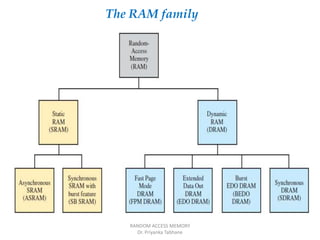
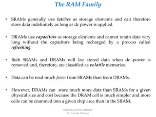
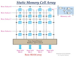
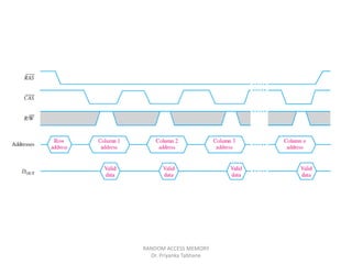
THIS PPT CONTAINS Definition,Principal components of a SM chart,ASM chart for combinational circuits,ASM chart in equivalent form,Example of development of ASM chart from Mealy Machine,Example of development of ASM chart from Moore Machine,Advantages of ASM chart
Memory organization in computer architectureFaisal Hussain
Memory organization in computer architecture
Volatile Memory
Non-Volatile Memory
Memory Hierarchy
Memory Access Methods
Random Access
Sequential Access
Direct Access
Main Memory
DRAM
SRAM
NVRAM
RAM: Random Access Memory
ROM: Read Only Memory
Auxiliary Memory
Cache Memory
Hit Ratio
Associative Memory
RAM (Random access memory) is the place in a computer where the operating system, application programs, and data in current use are kept so that they can be quickly reached by the computer's processor.
speech, hearing, noise, intelligibility, loudness, voice mechanism, threshold of ear, Fletcher Munson Curve, Counter curve of equal loudness, relation between loudness level and duration of time, calculation of loudness level
Loudspeaker- direct radiating type and horn type.pptxpriyankatabhane
loudspeaker, characteristics of loudspeaker, direct radiating type loudspeaker, permanent magnet type, cone type loudspeaker, moving coil type loudspeaker, dynamic loudspeaker, electrodynamic loudspeaker, horn loudspeaker
Environmental acoustics, speech interference level, how to calculate speech interference level, voice level, acoustics calibrator, types of acoustics calibrator, type 4228, type 4231, type 4297, type 3541 A, type 4226, type 4229
classical ray theory, growth and decay of sound in live and dead room, sound absorbing materials, their types and uses, porous material, public address system, howl round, under water acoustics, transmission losses in sea water
Fundamentals of Ultrasonic waves and applicationspriyankatabhane
ultrasonic waves, generation, properties, types, transducers, propagation in liquids, ultrasonic velocity, us absorption, relaxation in binary mixtures, normal and associated liquids. Measurement techniques: interfero method, optical method, sing around method , pulse echo technique, pulse echo overlap method. Application of us waves: cavitation effect, SONAR, us welding, us cleaning.
the topic of ultrasonic for MSc students. The topic covers : what are ultrasonic wave? the basic history about the waves. there properties, types, how to generate it, how to calculate the velocity of ultrasound in liquids, how does ultrasound interact with binary mixtures, the main applications of ultrasound.
Nutraceutical market, scope and growth: Herbal drug technologyLokesh Patil
As consumer awareness of health and wellness rises, the nutraceutical market—which includes goods like functional meals, drinks, and dietary supplements that provide health advantages beyond basic nutrition—is growing significantly. As healthcare expenses rise, the population ages, and people want natural and preventative health solutions more and more, this industry is increasing quickly. Further driving market expansion are product formulation innovations and the use of cutting-edge technology for customized nutrition. With its worldwide reach, the nutraceutical industry is expected to keep growing and provide significant chances for research and investment in a number of categories, including vitamins, minerals, probiotics, and herbal supplements.
Multi-source connectivity as the driver of solar wind variability in the heli...Sérgio Sacani
The ambient solar wind that flls the heliosphere originates from multiple
sources in the solar corona and is highly structured. It is often described
as high-speed, relatively homogeneous, plasma streams from coronal
holes and slow-speed, highly variable, streams whose source regions are
under debate. A key goal of ESA/NASA’s Solar Orbiter mission is to identify
solar wind sources and understand what drives the complexity seen in the
heliosphere. By combining magnetic feld modelling and spectroscopic
techniques with high-resolution observations and measurements, we show
that the solar wind variability detected in situ by Solar Orbiter in March
2022 is driven by spatio-temporal changes in the magnetic connectivity to
multiple sources in the solar atmosphere. The magnetic feld footpoints
connected to the spacecraft moved from the boundaries of a coronal hole
to one active region (12961) and then across to another region (12957). This
is refected in the in situ measurements, which show the transition from fast
to highly Alfvénic then to slow solar wind that is disrupted by the arrival of
a coronal mass ejection. Our results describe solar wind variability at 0.5 au
but are applicable to near-Earth observatories.
A brief information about the SCOP protein database used in bioinformatics.
The Structural Classification of Proteins (SCOP) database is a comprehensive and authoritative resource for the structural and evolutionary relationships of proteins. It provides a detailed and curated classification of protein structures, grouping them into families, superfamilies, and folds based on their structural and sequence similarities.
Seminar of U.V. Spectroscopy by SAMIR PANDASAMIR PANDA
Spectroscopy is a branch of science dealing the study of interaction of electromagnetic radiation with matter.
Ultraviolet-visible spectroscopy refers to absorption spectroscopy or reflect spectroscopy in the UV-VIS spectral region.
Ultraviolet-visible spectroscopy is an analytical method that can measure the amount of light received by the analyte.
THE IMPORTANCE OF MARTIAN ATMOSPHERE SAMPLE RETURN.Sérgio Sacani
The return of a sample of near-surface atmosphere from Mars would facilitate answers to several first-order science questions surrounding the formation and evolution of the planet. One of the important aspects of terrestrial planet formation in general is the role that primary atmospheres played in influencing the chemistry and structure of the planets and their antecedents. Studies of the martian atmosphere can be used to investigate the role of a primary atmosphere in its history. Atmosphere samples would also inform our understanding of the near-surface chemistry of the planet, and ultimately the prospects for life. High-precision isotopic analyses of constituent gases are needed to address these questions, requiring that the analyses are made on returned samples rather than in situ.
Introduction:
RNA interference (RNAi) or Post-Transcriptional Gene Silencing (PTGS) is an important biological process for modulating eukaryotic gene expression.
It is highly conserved process of posttranscriptional gene silencing by which double stranded RNA (dsRNA) causes sequence-specific degradation of mRNA sequences.
dsRNA-induced gene silencing (RNAi) is reported in a wide range of eukaryotes ranging from worms, insects, mammals and plants.
This process mediates resistance to both endogenous parasitic and exogenous pathogenic nucleic acids, and regulates the expression of protein-coding genes.
What are small ncRNAs?
micro RNA (miRNA)
short interfering RNA (siRNA)
Properties of small non-coding RNA:
Involved in silencing mRNA transcripts.
Called “small” because they are usually only about 21-24 nucleotides long.
Synthesized by first cutting up longer precursor sequences (like the 61nt one that Lee discovered).
Silence an mRNA by base pairing with some sequence on the mRNA.
Discovery of siRNA?
The first small RNA:
In 1993 Rosalind Lee (Victor Ambros lab) was studying a non- coding gene in C. elegans, lin-4, that was involved in silencing of another gene, lin-14, at the appropriate time in the
development of the worm C. elegans.
Two small transcripts of lin-4 (22nt and 61nt) were found to be complementary to a sequence in the 3' UTR of lin-14.
Because lin-4 encoded no protein, she deduced that it must be these transcripts that are causing the silencing by RNA-RNA interactions.
Types of RNAi ( non coding RNA)
MiRNA
Length (23-25 nt)
Trans acting
Binds with target MRNA in mismatch
Translation inhibition
Si RNA
Length 21 nt.
Cis acting
Bind with target Mrna in perfect complementary sequence
Piwi-RNA
Length ; 25 to 36 nt.
Expressed in Germ Cells
Regulates trnasposomes activity
MECHANISM OF RNAI:
First the double-stranded RNA teams up with a protein complex named Dicer, which cuts the long RNA into short pieces.
Then another protein complex called RISC (RNA-induced silencing complex) discards one of the two RNA strands.
The RISC-docked, single-stranded RNA then pairs with the homologous mRNA and destroys it.
THE RISC COMPLEX:
RISC is large(>500kD) RNA multi- protein Binding complex which triggers MRNA degradation in response to MRNA
Unwinding of double stranded Si RNA by ATP independent Helicase
Active component of RISC is Ago proteins( ENDONUCLEASE) which cleave target MRNA.
DICER: endonuclease (RNase Family III)
Argonaute: Central Component of the RNA-Induced Silencing Complex (RISC)
One strand of the dsRNA produced by Dicer is retained in the RISC complex in association with Argonaute
ARGONAUTE PROTEIN :
1.PAZ(PIWI/Argonaute/ Zwille)- Recognition of target MRNA
2.PIWI (p-element induced wimpy Testis)- breaks Phosphodiester bond of mRNA.)RNAse H activity.
MiRNA:
The Double-stranded RNAs are naturally produced in eukaryotic cells during development, and they have a key role in regulating gene expression .
This pdf is about the Schizophrenia.
For more details visit on YouTube; @SELF-EXPLANATORY;
https://www.youtube.com/channel/UCAiarMZDNhe1A3Rnpr_WkzA/videos
Thanks...!
Observation of Io’s Resurfacing via Plume Deposition Using Ground-based Adapt...Sérgio Sacani
Since volcanic activity was first discovered on Io from Voyager images in 1979, changes
on Io’s surface have been monitored from both spacecraft and ground-based telescopes.
Here, we present the highest spatial resolution images of Io ever obtained from a groundbased telescope. These images, acquired by the SHARK-VIS instrument on the Large
Binocular Telescope, show evidence of a major resurfacing event on Io’s trailing hemisphere. When compared to the most recent spacecraft images, the SHARK-VIS images
show that a plume deposit from a powerful eruption at Pillan Patera has covered part
of the long-lived Pele plume deposit. Although this type of resurfacing event may be common on Io, few have been detected due to the rarity of spacecraft visits and the previously low spatial resolution available from Earth-based telescopes. The SHARK-VIS instrument ushers in a new era of high resolution imaging of Io’s surface using adaptive
optics at visible wavelengths.
2. RAM
The Random-Access Memory
• A RAM is a read/write memory in which data can be written
into or read from any selected address in any sequence.
• When a data unit is written into a given address in the RAM,
the data unit previously stored at that address is replaced by
the new data unit.
• When a data unit is read from a given address in the RAM,
the data unit remains stored and is not erased by the read
operation.
• This non destructive read operation can be viewed as copying
the content of an address while leaving the content intact.
• A RAM is typically used for short-term data storage because
it cannot retain stored data when power is turned off.
RANDOM ACCESS MEMORY
Dr. Priyanka Tabhane
4. The RAM Family
• SRAMs generally use latches as storage elements and can therefore
store data indefinitely as long as dc power is applied.
• DRAMs use capacitors as storage elements and cannot retain data very
long without the capacitors being recharged by a process called
refreshing.
• Both SRAMs and DRAMs will lose stored data when dc power is
removed and, therefore, are classified as volatile memories.
• Data can be read much faster from SRAMs than from DRAMs.
• However, DRAMs can store much more data than SRAMs for a given
physical size and cost because the DRAM cell is much simpler and more
cells can be crammed into a given chip area than in the SRAM.
RANDOM ACCESS MEMORY
Dr. Priyanka Tabhane
5. Static/bipolar RAMs (SRAMs)
Memory Cell
• All SRAMs are characterized by latch memory cells. As
long as dc power is applied to a static memory cell, it can
retain a 1 or 0 state indefinitely.
• If power is removed, the stored data bit is lost.
A typical SRAM latch memory cell
RANDOM ACCESS MEMORY
Dr. Priyanka Tabhane
6. • a basic SRAM latch memory
cell.
• The cell is selected by an
active level on the Select line
and a data bit (1 or 0) is
written into the cell by placing
it on the Data in line.
• A data bit is read by taking it
off the Data out line.
A typical SRAM latch memory cell
RANDOM ACCESS MEMORY
Dr. Priyanka Tabhane
7. Static Memory Cell Array
Basic SRAM array
RANDOM ACCESS MEMORY
Dr. Priyanka Tabhane
8. Static Memory Cell Array
• The memory cells in a SRAM are organized in rows and
columns, for the case of an n x 4 array.
• All the cells in a row share the same Row Select line.
• Each set of Data in and Data out lines go to each cell in a
given column and are connected to a single data line that
serves as both an input and output (Data I/O) through the
data input and data output buffers.
• To write a data unit, in this case a nibble (4 bits), into a given
row of cells in the memory array, the Row Select line is taken
to its active state and four data bits are placed on the Data I/O
lines.
• The Write line is then taken to its active state, which causes
each data bit to be stored in a selected cell in the associated
column.
• To read a data unit, the Read line is taken to its active state,
which causes the four data bits stored in the selected row to
appear on the Data I/O lines.
RANDOM ACCESS MEMORY
Dr. Priyanka Tabhane
9. Basic Asynchronous
SRAM Organization
• An asynchronous SRAM is
one in which the operation
is not synchronized with a
system clock.
• Figure shows the general
organization of a SRAM, a
32k * 8 bit memory is used.
RANDOM ACCESS MEMORY
Dr. Priyanka Tabhane
10. • In the READ mode, the eight data bits that are stored in a selected
address appear on the data output lines.
• In the WRITE mode, the eight data bits that are applied to the data
input lines are stored at a selected address.
• The data input and data output lines (I/O 0 through I/O 7) share the
same lines.
• During READ, they act as output lines (O0 through O7) and during
WRITE they act as input lines (I0 through I7).
RANDOM ACCESS MEMORY
Dr. Priyanka Tabhane
11. Tri-state Outputs
• Tri-state buffers in a memory allow the data lines to act
as either input or output lines and connect the memory
to the data bus in a computer.
• These buffers have three output states: HIGH (1), LOW
(0), and HIGH-Z (open).
• Tri-state outputs are indicated on logic symbols by a small
inverted triangle ( ) .
RANDOM ACCESS MEMORY
Dr. Priyanka Tabhane
12. Buses
• A bus is one or more conductive paths that serve to interconnect
two or more functional components of a system or several diverse
systems.
• a bus is a collection of specified voltage levels and/or current levels
and signals that allow various devices to communicate and work
properly together.
• A microprocessor is connected to memories and input/output
devices by certain bus structures.
• An address bus allows the microprocessor to address the memories,
and a data bus provides for transfer of data between the
microprocessor, the memories, and the input/output devices such
as monitors, printers, keyboards, and modems.
• A control bus allows the microprocessor to control data transfers
and timing for the various components.
RANDOM ACCESS MEMORY
Dr. Priyanka Tabhane
13. Dynamic RAM (DRAM) Memory Cells
• Dynamic memory cells store a data bit in a small
capacitor rather than in a latch.
• The advantage of this type of cell is that it is very simple,
thus allowing very large memory arrays to be
constructed on a chip at a lower cost per bit.
• The disadvantage is that the storage capacitor cannot
hold its charge over an extended period of time and will
lose the stored data bit unless its charge is refreshed
periodically.
• To refresh requires additional memory circuitry and
complicates the operation of the DRAM.
RANDOM ACCESS MEMORY
Dr. Priyanka Tabhane
14. RANDOM ACCESS MEMORY
Dr. Priyanka Tabhane
Figure shows a typical DRAM cell consisting of a
single MOS transistor (MOSFET) and a capacitor.
In this type of cell, the transistor acts as a switch.
15. • A LOW on the R/W line (WRITE
mode) enables the tri-state input
buffer and disables the output
buffer.
• For a 1 to be written into the cell,
the DIN line must be HIGH, and
the transistor must be turned on
by a HIGH on the row line.
• The transistor acts as a closed
switch connecting the capacitor to
the bit line.
• This connection allows the
capacitor to charge to a positive
voltage.
RANDOM ACCESS MEMORY
Dr. Priyanka Tabhane
Writing a 1 into the memory cell
Simplified operation of cell
16. • When a 0 is to be stored, a LOW is
applied to the DIN line.
• If the capacitor is storing a 0, it
remains uncharged, or if it is
storing a 1, it discharges.
• When the row line is taken back
LOW, the transistor turns off and
disconnects the capacitor from the
bit line, thus “trapping” the charge
(1 or 0) on the capacitor
RANDOM ACCESS MEMORY
Dr. Priyanka Tabhane
Writing a 0 into the memory cell
17. • To read from the cell, the R/W
(Read/Write) line is HIGH,
enabling the output buffer and
disabling the input buffer.
• When the row line is taken
HIGH, the transistor turns on
and connects the capacitor to the
bit line and thus to the output
buffer (sense amplifier),so the
data bit appears on the data-
output line (DOUT).
RANDOM ACCESS MEMORY
Dr. Priyanka Tabhane
Reading a 1 from the memory cell
18. • For refreshing the memory cell,
the R/W line is HIGH, the row line
is HIGH, and the refresh line is
HIGH.
• The transistor turns on,
connecting the capacitor to the bit
line.
• The output buffer is enabled, and
the stored data bit is applied to
the input of the refresh buffer,
which is enabled by the HIGH on
the refresh input.
• This produces a voltage on the bit
line corresponding to the stored
bit, thus replenishing the
capacitor.
RANDOM ACCESS MEMORY
Dr. Priyanka Tabhane
Refreshing a stored 1
19. DRAM Organization
RANDOM ACCESS MEMORY
Dr. Priyanka Tabhane
• The major application of DRAMs is in the main memory of
computers.
• The difference between DRAMs and SRAMs is the type of memory
cell.
• DRAM memory cell consists of one transistor and a capacitor and is
much simpler than the SRAM cell.
• This allows much greater densities in DRAMs and results in greater
bit capacities for a given chip area, although much slower access
time.
• As charge stored in a capacitor will leak off, the DRAM cell requires
a frequent refresh operation to preserve the stored data bit.
• This requirement results in more complex circuitry than in a SRAM.
20. Address Multiplexing
• DRAMs use a technique called address multiplexing to reduce the
number of address lines.
• The ten address lines are time multiplexed at the beginning of a
memory cycle by the row address select (RAS) and the column address
select (CAS) into two separate 10-bit address fields.
• First, the 10-bit row address is latched into the row address register.
• Next, the 10-bit column address is latched into the column address
register.
• The row address and the column address are decoded to select one
of the 1,048,576 addresses (2^20 = 1,048,576) in the memory array.
• The basic timing for the address multiplexing operation is shown in
Figure.
RANDOM ACCESS MEMORY
Dr. Priyanka Tabhane
21. Read and Write Cycles
• At the beginning of each read or write memory cycle,
RAS and CAS go active (LOW) to multiplex the row and
column addresses into the registers, and decoders.
• For a read cycle, the R/W input is HIGH. For a write cycle,
the R/W input is LOW.
RANDOM ACCESS MEMORY
Dr. Priyanka Tabhane
24. Fast Page Mode
• In the normal read or write cycle described previously, the row address
for a particular memory location is first loaded by an active-LOW RAS
and then the column address for that location is loaded by an active-LOW
CAS.
• The next location is selected by another RAS followed by a CAS, and so on.
• A “page” is a section of memory available at a single row address and
consists of all the columns in a row.
• Fast page mode allows fast successive read or write operations at each
column address in a selected row.
• A row address is first loaded by RAS going LOW and remaining LOW
while CAS is toggled between HIGH and LOW.
RANDOM ACCESS MEMORY
Dr. Priyanka Tabhane
25. • A single row address is selected and remains selected while RAS is
active.
• Each successive CAS selects another column in the selected row.
• So, after a fast page mode cycle, all of the addresses in the selected
row have been read from or written into, depending on R/W.
• For example, a fast page mode cycle for the DRAM in Figure requires
CAS to go active 1024 times for each row selected by RAS.
• Fast page mode operation for read is illustrated by the timing
diagram
• When CAS goes to its non asserted state (HIGH), it disables the data
outputs.
• Therefore, the transition of CAS to HIGH must occur only after valid
data are latched by the external system.
RANDOM ACCESS MEMORY
Dr. Priyanka Tabhane
27. Refresh Cycles
• DRAMs are based on capacitor charge storage for each bit in the
memory array.
• This charge degrades (leaks off) with time and temperature, so each bit
must be periodically refreshed (recharged) to maintain the correct bit
state.
• A DRAM must be refreshed every several milliseconds.
• A read operation automatically refreshes all the addresses in the
selected row.
• you cannot always predict how often there will be a read cycle, and so
you cannot depend on a read cycle to occur frequently enough to
prevent data loss.
• Therefore, special refresh cycles must be implemented in DRAM
systems.
RANDOM ACCESS MEMORY
Dr. Priyanka Tabhane
28. • The two types of refresh operations are RAS only refresh and CAS before
RAS refresh.
• RAS-only refresh consists of a RAS transition to the LOW (active) state,
which latches the address of the row to be refreshed while CAS remains
HIGH (inactive) throughout the cycle.
• An external counter is used to provide the row addresses for this type
of operation.
• The CAS before RAS refresh is initiated by CAS going LOW before RAS goes
LOW.
• This sequence activates an internal refresh counter that generates the
row address to be refreshed.
• This address is switched by the data selector into the row decoder.
RANDOM ACCESS MEMORY
Dr. Priyanka Tabhane
30. Types of DRAMs
• Fast Page Mode (FPM) DRAM
• the Extended Data Out (EDO) DRAM,
• the Burst Extended Data Out (BEDO) DRAM,
• the Synchronous (S) DRAM.
RANDOM ACCESS MEMORY
Dr. Priyanka Tabhane
31. FPM DRAM
• Fast page mode operation - a page in memory is all of the column
addresses contained within one row address.
• Addresses to be accessed are in the same row (on the same page).
• FPM saves time over pure random accessing because in FPM the
row address is specified only once for access to several successive
column addresses whereas for pure random accessing, a row
address is specified for each column address.
• the CAS signal has to wait until the valid data from a given address are
accepted (latched) by the external system (CPU) before it can go to
its non asserted state.
• When CAS goes to its non asserted state, the data outputs are disabled.
• This means that the next column address cannot occur until after
the data from the current column address are transferred to the
CPU.
• This limits the rate at which the columns within a page can be
addressed.
RANDOM ACCESS MEMORY
Dr. Priyanka Tabhane
32. EDO DRAM
• The Extended Data Out DRAM, sometimes called hyper
page mode DRAM, is similar to the FPM DRAM.
• The key difference is that the CAS signal in the EDO
DRAM does not disable the output data when it goes to
its non asserted state because the valid data from the
current address can be held until CAS is asserted again.
• This means that the next column address can be accessed
before the external system accepts the current valid data.
• The idea is to speed up the access time.
RANDOM ACCESS MEMORY
Dr. Priyanka Tabhane
33. BEDO DRAM
• The Burst Extended Data Out DRAM is an EDO DRAM
with address burst capability.
• the address burst allows up to four addresses to be
internally generated from a single external address,
which saves some access time.
• This same concept applies to the BEDO DRAM.
RANDOM ACCESS MEMORY
Dr. Priyanka Tabhane
34. SDRAM
• Faster DRAMs are needed to keep up with the ever-increasing
speed of microprocessors.
• The Synchronous DRAM is one way to accomplish this.
• the operation of the SDRAM is synchronized with the system
clock, which also runs the microprocessor in a computer system.
• With asynchronous memories, the microprocessor must wait for the
DRAM to complete its internal operations.
• However, with synchronous operation, the DRAM latches
addresses, data, and control information from the processor under
control of the system clock.
• This allows the processor to handle other tasks while the memory
read/write operations are in progress, rather than having to wait for
the memory to do its thing as is the case in asynchronous systems.
RANDOM ACCESS MEMORY
Dr. Priyanka Tabhane
35. DDR SDRAM
• DDR stands for double data rate.
• A DDR SDRAM is clocked on both edges of a clock pulse,
whereas a SDRAM is clocked on only one edge.
• Because of the double clocking, a DDR SDRAM is
theoretically twice as fast as an SDRAM.
• Sometimes the SDRAM is referred to as an SDR SDRAM
(single data rate SDRAM) for contrast with the DDR
SDRAM.
RANDOM ACCESS MEMORY
Dr. Priyanka Tabhane
36. Assignment
• List two types of SRAM.
• Explain how SRAMs and DRAMs differ.
• Explain basic organization of SRAM
• Explain operation in DRAM.
• Describe the refresh operation in a DRAM.
• List four types of DRAM.
• What are tri state outputs ?
• Write a note on FPM DRAM.
RANDOM ACCESS MEMORY
Dr. Priyanka Tabhane