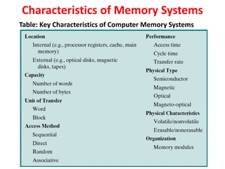
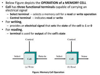
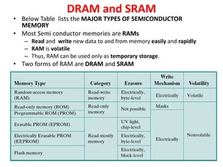
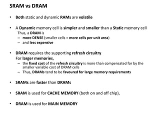
UNIT 5
MEMORIES
Characteristics of Memory Systems
Table: Key Characteristics of Computer Memory Systems
The Memory Hierarchy
• Typical Memory Hierarchy is illustrated in Figure
As one goes DOWN the hierarchy,
the following occur:
a. Decreasing cost per bit
b. Increasing capacity
c. Increasing access time
d. Decreasing frequency of access
of the memory by the processor
• Below Figure depicts the OPERATION of a MEMORY CELL
• Cell has three functional terminals capable of carrying an
electrical signal
– Select terminal -- selects a memory cell for a read or write operation
– Control terminal -- indicates read or write
• For writing,
– provides an electrical signal that sets the state of the cell to 1 or 0
• For reading,
– terminal is used for output of the cell’s state
Figure: Memory Cell Operation
DRAM and SRAM
• Below Table lists the MAJOR TYPES OF SEMICONDUCTOR
MEMORY
• Most Semi conductor memories are RAMs
– Read and write new data to and from memory easily and rapidly
– RAM is volatile
– Thus, RAM can be used only as temporary storage.
• Two forms of RAM are DRAM and SRAM
Memory is primarily of three types −
Cache Memory
Primary Memory/Main Memory
Secondary Memory
SRAM vs DRAM
• Both static and dynamic RAMs are volatile
• A Dynamic memory cell is simpler and smaller than a Static memory cell
Thus, a DRAM is
– more DENSE (smaller cells = more cells per unit area)
– and less expensive
• DRAM requires the supporting refresh circuitry
For larger memories,
– the fixed cost of the refresh circuitry is more than compensated for by the
smaller variable cost of DRAM cells
– Thus, DRAMs tend to be favoured for large memory requirements
• SRAMs are faster than DRAMs
• SRAM is used for CACHE MEMORY (both on and off chip),
• DRAM is used for MAIN MEMORY
Write Operation
1) BL= i/p
2) WL= 1
3) BL= 1; Cs= Vdd (Charging)
4) BL= 0; Cs= 0 (Discharging)
ROM Design
ROM Size:
No. of i/p= n
Size of each address/word size= m
Eg. n=4, m=4
16x4=64 bits= (64/8)bytes= 8bytes
ROM Structure:
1) Decoder+ Programmable OR gates
2) AND Gates (fixed)+ Programable
OR gates
ROM Design
Storage
device/memory in
which Fixed set of
binary data are
stored
Design a combinational circuit using ROM. The circuit accept a 3-bit
number and outputs a binary number equal to the square of the input
number.
Design a combinational circuit using ROM. The circuit accept a 3-bit number
and outputs a binary number equal to the square of the input number.
UNIT 5 MEMORY.pdf
UNIT 5 MEMORY.pdf
UNIT 5 MEMORY.pdf

UNIT 5 MEMORY.pdf

  • 1.
  • 2.
    Characteristics of MemorySystems Table: Key Characteristics of Computer Memory Systems
  • 3.
    The Memory Hierarchy •Typical Memory Hierarchy is illustrated in Figure As one goes DOWN the hierarchy, the following occur: a. Decreasing cost per bit b. Increasing capacity c. Increasing access time d. Decreasing frequency of access of the memory by the processor
  • 4.
    • Below Figuredepicts the OPERATION of a MEMORY CELL • Cell has three functional terminals capable of carrying an electrical signal – Select terminal -- selects a memory cell for a read or write operation – Control terminal -- indicates read or write • For writing, – provides an electrical signal that sets the state of the cell to 1 or 0 • For reading, – terminal is used for output of the cell’s state Figure: Memory Cell Operation
  • 5.
    DRAM and SRAM •Below Table lists the MAJOR TYPES OF SEMICONDUCTOR MEMORY • Most Semi conductor memories are RAMs – Read and write new data to and from memory easily and rapidly – RAM is volatile – Thus, RAM can be used only as temporary storage. • Two forms of RAM are DRAM and SRAM
  • 6.
    Memory is primarilyof three types − Cache Memory Primary Memory/Main Memory Secondary Memory
  • 14.
    SRAM vs DRAM •Both static and dynamic RAMs are volatile • A Dynamic memory cell is simpler and smaller than a Static memory cell Thus, a DRAM is – more DENSE (smaller cells = more cells per unit area) – and less expensive • DRAM requires the supporting refresh circuitry For larger memories, – the fixed cost of the refresh circuitry is more than compensated for by the smaller variable cost of DRAM cells – Thus, DRAMs tend to be favoured for large memory requirements • SRAMs are faster than DRAMs • SRAM is used for CACHE MEMORY (both on and off chip), • DRAM is used for MAIN MEMORY
  • 16.
    Write Operation 1) BL=i/p 2) WL= 1 3) BL= 1; Cs= Vdd (Charging) 4) BL= 0; Cs= 0 (Discharging)
  • 26.
    ROM Design ROM Size: No.of i/p= n Size of each address/word size= m Eg. n=4, m=4 16x4=64 bits= (64/8)bytes= 8bytes ROM Structure: 1) Decoder+ Programmable OR gates 2) AND Gates (fixed)+ Programable OR gates
  • 28.
    ROM Design Storage device/memory in whichFixed set of binary data are stored
  • 30.
    Design a combinationalcircuit using ROM. The circuit accept a 3-bit number and outputs a binary number equal to the square of the input number.
  • 31.
    Design a combinationalcircuit using ROM. The circuit accept a 3-bit number and outputs a binary number equal to the square of the input number.