Downloaded 12 times

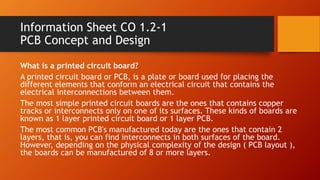


![Information Sheet CO 1.2-1
PCB Concept and Design
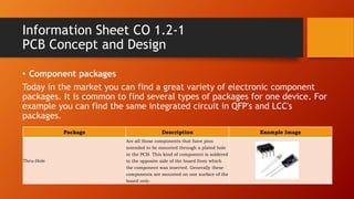
Package Description Example Image
SMD/SMT (surface mount device/surface
mount technology)
Are all those components that are soldered in the same side of the board
from which the component was placed. The advantage of this type of
package is that it can be mounted on both sides of the PCB. Also, these
components are smaller than the thru-hole type, which allows the design
of smaller and denser printed circuit boards. These types of components
are useful for frequencies up to 200 [MHz] (fundamental clock frequency).
BGA (Ball grid array)
These types of components are frequently used for high density pin
integrated circuits. For soldering them to the printed circuit boards it is
required to have specialized machinery due that the pins are made of
solder balls that have to be melted for making the electrical contact with
the pads.
BGA components are ideal for high frequency integrated circuits due to
the very small parasitic inductances present in the joint between the pad
and the balls. These type of components are very common in computer
hardware like motherboards and video accelerator cards.](https://image.slidesharecdn.com/learningoutcome2preparemakepcbmodules-200617121434/85/Learning-outcome-2-prepare-make-pcb-modules-10-320.jpg)


A printed circuit board (PCB) contains copper tracks that connect electronic components. PCBs can have multiple layers of tracks separated by insulating layers. Components connect to pads on the PCB surface or pass through holes. Manufacturing involves designing circuitry, creating a mask, and etching away unwanted copper. Safety precautions must be followed when using chemicals.