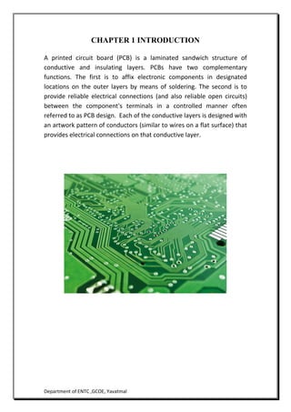
This document is a seminar report on PCB design submitted by Sadguru Kishor Lonari to the Department of Electronics and Telecommunication Engineering at Government College of Engineering, Yavatmal. The report provides an overview of printed circuit boards, including their history and development, common types of PCB layers, components required for manufacturing, and the basic steps involved in the PCB design and manufacturing process. It discusses applications of PCBs and analyzes their advantages and disadvantages. The conclusion discusses potential future enhancements to PCB design technologies.