Download to read offline
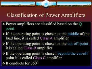
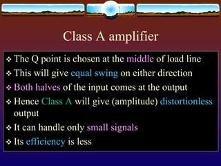

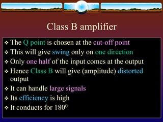

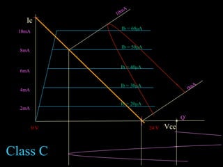


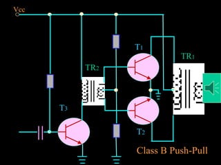
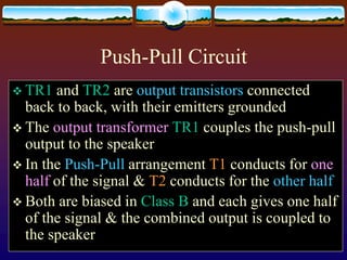


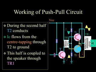
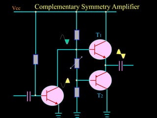


Power amplifiers are classified based on their operating point as Class A, B, or C. Class A amplifiers have their operating point at the middle of the load line, resulting in distortionless output but lower efficiency. Class B amplifiers have their operating point at the cut-off point, handling larger signals with higher efficiency but distorted output. Class C amplifiers operate beyond the cut-off point, severely distorting the output. Class A amplifiers are suitable for audio but cannot handle large signals, so Class B push-pull amplifiers using two amplifiers are often used instead to produce an undistorted output. Complementary symmetry amplifiers avoid using transformers by employing an NPN and PNP transistor at the output


