SlideShare a Scribd company logo
1 of 20
– MOSFETPOWER TRANSISTOR
Example of power MOSFET parameters;
Parameter 2N675
7
2N679
2
VDS(max) (V) 150 400
ID(max) (A) - @ T = 25C 8 2
PD (W) 75 20
– MOSFETPOWER TRANSISTOR
The superior characteristics of MOSFETs are;
• Faster switching time;
• No second breakdown;
• Stable gain and response time over a wide temperature
range (Figure on the next slide).
– MOSFETPOWER TRANSISTOR
Transconductance
versus drain current
curves for various
values of temperature
– less than the
variation in BJT
current gain.
– MOSFETPOWER TRANSISTOR
Transfer
characteristics curves
for various values of
temperature.
– MOSFETPOWER TRANSISTOR
Structure
– MOSFETPOWER TRANSISTOR
Structure
DMOS process can
be used to produce a
large number of
hexagonal cells on a
single chip.
– MOSFETPOWER TRANSISTOR
Structure
These hexagonal cells
can be paralleled to
form large-area
devices without the
need of emitter ballast
resistance.
A single power
MOSFET may contain
as many as 25,000
parallel cells.
– MOSFETPOWER TRANSISTOR
The “ON” resistive
path between drain
and source (rds(on))
is an important
parameter in
power capability of
MOSFET
– ComparisonPOWER TRANSISTOR
BJT
Requires complex input
circuitry because of high
input current (current-
controlled device)
More sensitive to
temperature variation –
thermal runaway and
problem of second
breakdown.
MOSFET
Simple input circuitry
because of low input
current (voltage-controlled
device).
More immune to thermal
runaway and second
breakdown.
– Heat sinksPOWER TRANSISTOR
• The power dissipated in a transistor can cause an
internal temperature rise above ambient temperature.
• This heat, if not properly removed, may cause internal
temperature above a safe limit and can cause
permanent damage to transistor.
• Heat may be removed through proper packaging:
– Heat sinksPOWER TRANSISTOR
• Additionally, heat sinks can be used to remove the heat
developed in the transistor:
Heat sinks (Extra)POWER TRANSISTOR
Electrical equivalent
circuit of thermal-
conduction process
JADAJ PTT 
JT Temperature of transistor
junction
AT Ambient temperature
AJ TT  Temperature difference
 Voltage difference
JA Thermal resistance between the junction and ambient
 Electrical resistance
DP Thermal power through the element
 Electric current.
Heat sinks (Extra)POWER TRANSISTOR
Manufacturers’ data
sheet for power
devices generally
give:
• maximum operating
junction (device)
temperature, TJmax;
• thermal resistance
from the junction to
the case, JC;
The temperature conduction
process may be represented
as follows:
POWER TRANSISTOR
The following equation can be
used to describe the
temperature conduction
process:
ambdev TT 
 amb-snksnkcasecasedev   DP
If the heat sink is not used, then;
 ambcasecasedevambdev   DPTT
Heat sinks (Extra)
Heat sinks (Extra)POWER TRANSISTOR
A MOSFET has the following parameters;
C/W;75.1casedev


Determine the maximum power dissipation in the
transistor and determine the temperature of the transistor
case and heat sink.
EXAMPLE 8.3
C/W;1snk-case


C/W;5amb-snk

 C/W;50amb-case


C;150devmax

 TTJ C;30amb

T
Heat sinks (Extra)POWER TRANSISTOR
EXAMPLE 8.3 – Solution
Maximum power (without heat sink)
W32.2
5075.1
30150
amb-casecase-dev
ambmax
max 







TT
P J
D
Maximum power (with heat sink)
amb-snksnk-casecase-dev
ambmax
max
 


TT
P J
D
W5.15
5175.1
30150




Heat sinks (Extra)POWER TRANSISTOR
EXAMPLE 8.3 – Solution (cont’d)
Heat sink temperature
amb-snkmaxambsnk DPTT 
amb-snkmaxambsnk DPTT 
C5.10755.1530 

Heat sinks (Extra)POWER TRANSISTOR
EXAMPLE 8.3 – Solution (cont’d)
Case temperature
 amb-snksnk-casemaxambcase   DPTT
 amb-snksnk-casemaxambcase   DPTT
  C123515.1530 

Note: The use of heat sink allows
more power to be dissipated in the
device.
Heat sinks (Extra)POWER TRANSISTOR
Power derating curve
Manufacturer usually specifies:
• the maximum temperature TJmax;
• the maximum power dissipation PDmax, at a particular
ambient temperature TA0 (usually 25C); and
• the thermal resistance JA.
In addition, a graph – power derating curve is provided.
Heat sinks (Extra)POWER TRANSISTOR
Power derating curve
For operation below
TA0, the device can
safely dissipate the
rated value of PD0
watts.
If the device is to be operated at higher ambient
temperature, the maximum allowable power dissipation
must be derated according to the straight line.

More Related Content

What's hot

Transistor bias circuit
Transistor bias circuitTransistor bias circuit
Transistor bias circuit
Adk Adool
 
EE452_Open Loop Buck Converter
EE452_Open Loop Buck ConverterEE452_Open Loop Buck Converter
EE452_Open Loop Buck Converter
ki hei chan
 
Design and implementation of cyclo converter for high frequency applications
Design and implementation of cyclo converter for high frequency applicationsDesign and implementation of cyclo converter for high frequency applications
Design and implementation of cyclo converter for high frequency applications
cuashok07
 

What's hot (19)

Power Electtronics
Power ElecttronicsPower Electtronics
Power Electtronics
 
FET Biasing
FET BiasingFET Biasing
FET Biasing
 
Voltage series feedback
Voltage series feedbackVoltage series feedback
Voltage series feedback
 
L9 thyristor gate characteristics...contd
L9 thyristor gate characteristics...contdL9 thyristor gate characteristics...contd
L9 thyristor gate characteristics...contd
 
Lec17 mosfet iv
Lec17 mosfet ivLec17 mosfet iv
Lec17 mosfet iv
 
Design of 4-stage Marx generator using gas discharge tube
Design of 4-stage Marx generator using gas discharge tubeDesign of 4-stage Marx generator using gas discharge tube
Design of 4-stage Marx generator using gas discharge tube
 
Mosfet baising
Mosfet baisingMosfet baising
Mosfet baising
 
Transistor bias circuit
Transistor bias circuitTransistor bias circuit
Transistor bias circuit
 
Small signal analysis of bjt amplifiers
Small signal analysis of bjt amplifiersSmall signal analysis of bjt amplifiers
Small signal analysis of bjt amplifiers
 
Unit 4 cycloconverter
Unit 4 cycloconverterUnit 4 cycloconverter
Unit 4 cycloconverter
 
L11 rc triggering circuit
L11 rc triggering circuitL11 rc triggering circuit
L11 rc triggering circuit
 
EE452_Open Loop Buck Converter
EE452_Open Loop Buck ConverterEE452_Open Loop Buck Converter
EE452_Open Loop Buck Converter
 
Buck boost converter
Buck boost converterBuck boost converter
Buck boost converter
 
Transformerless buckboost converter by SEPURI
Transformerless buckboost converter by SEPURITransformerless buckboost converter by SEPURI
Transformerless buckboost converter by SEPURI
 
A basic presentation on cycloconverter
A basic presentation on cycloconverterA basic presentation on cycloconverter
A basic presentation on cycloconverter
 
Cycloconverter ppt
Cycloconverter pptCycloconverter ppt
Cycloconverter ppt
 
Automatic Night Light/ Street Light
Automatic Night Light/ Street LightAutomatic Night Light/ Street Light
Automatic Night Light/ Street Light
 
Design and implementation of cyclo converter for high frequency applications
Design and implementation of cyclo converter for high frequency applicationsDesign and implementation of cyclo converter for high frequency applications
Design and implementation of cyclo converter for high frequency applications
 
Hybrid converter
Hybrid converterHybrid converter
Hybrid converter
 

Similar to 5685802

Power electronics
Power electronicsPower electronics
Power electronics
psksiva13
 

Similar to 5685802 (20)

Datasheet 1
Datasheet 1Datasheet 1
Datasheet 1
 
High Power Density Multi-Mosfet-Based Series Resonant Inverter for Induction ...
High Power Density Multi-Mosfet-Based Series Resonant Inverter for Induction ...High Power Density Multi-Mosfet-Based Series Resonant Inverter for Induction ...
High Power Density Multi-Mosfet-Based Series Resonant Inverter for Induction ...
 
2011 Protection of a 3.3V Domain and Switchable 1.8V/3.3V I/O in 40nm and 28n...
2011 Protection of a 3.3V Domain and Switchable 1.8V/3.3V I/O in 40nm and 28n...2011 Protection of a 3.3V Domain and Switchable 1.8V/3.3V I/O in 40nm and 28n...
2011 Protection of a 3.3V Domain and Switchable 1.8V/3.3V I/O in 40nm and 28n...
 
Datasheet
DatasheetDatasheet
Datasheet
 
Bandgap Reference circuit Baased on FinFET Device
Bandgap Reference circuit Baased on FinFET DeviceBandgap Reference circuit Baased on FinFET Device
Bandgap Reference circuit Baased on FinFET Device
 
TOWARDS TEMPERATURE-INSENSITIVE NANOSCALE CMOS CIRCUITS WITH ADAPTIVELY REGUL...
TOWARDS TEMPERATURE-INSENSITIVE NANOSCALE CMOS CIRCUITS WITH ADAPTIVELY REGUL...TOWARDS TEMPERATURE-INSENSITIVE NANOSCALE CMOS CIRCUITS WITH ADAPTIVELY REGUL...
TOWARDS TEMPERATURE-INSENSITIVE NANOSCALE CMOS CIRCUITS WITH ADAPTIVELY REGUL...
 
EEL782_Project
EEL782_ProjectEEL782_Project
EEL782_Project
 
Power electronics
Power electronicsPower electronics
Power electronics
 
RPI_Research_Overview
RPI_Research_OverviewRPI_Research_Overview
RPI_Research_Overview
 
TOWARDS TEMPERATURE-INSENSITIVE NANOSCALE CMOS CIRCUITS WITH ADAPTIVELY REGUL...
TOWARDS TEMPERATURE-INSENSITIVE NANOSCALE CMOS CIRCUITS WITH ADAPTIVELY REGUL...TOWARDS TEMPERATURE-INSENSITIVE NANOSCALE CMOS CIRCUITS WITH ADAPTIVELY REGUL...
TOWARDS TEMPERATURE-INSENSITIVE NANOSCALE CMOS CIRCUITS WITH ADAPTIVELY REGUL...
 
Modified T-type topology of three-phase multi-level inverter for photovoltaic...
Modified T-type topology of three-phase multi-level inverter for photovoltaic...Modified T-type topology of three-phase multi-level inverter for photovoltaic...
Modified T-type topology of three-phase multi-level inverter for photovoltaic...
 
Original N-CHANNEL IGBT GB10NC60KD STGB10NC60KDT4 10A 600V TO-263 New STMicro...
Original N-CHANNEL IGBT GB10NC60KD STGB10NC60KDT4 10A 600V TO-263 New STMicro...Original N-CHANNEL IGBT GB10NC60KD STGB10NC60KDT4 10A 600V TO-263 New STMicro...
Original N-CHANNEL IGBT GB10NC60KD STGB10NC60KDT4 10A 600V TO-263 New STMicro...
 
Original N - Channel Mosfet IRFR3709ZTRPBF FR3709Z 3709 FR3709 TO-252 New IR
Original N - Channel Mosfet  IRFR3709ZTRPBF FR3709Z 3709 FR3709 TO-252 New IROriginal N - Channel Mosfet  IRFR3709ZTRPBF FR3709Z 3709 FR3709 TO-252 New IR
Original N - Channel Mosfet IRFR3709ZTRPBF FR3709Z 3709 FR3709 TO-252 New IR
 
System-level ESD protection of high-voltage tolerant IC pins – A case study
System-level ESD protection of high-voltage tolerant IC pins – A case study System-level ESD protection of high-voltage tolerant IC pins – A case study
System-level ESD protection of high-voltage tolerant IC pins – A case study
 
Original MOSFET N-CHANNEL FQPF11N70 11N70 TO-220 11A 700V New Fairchild
Original MOSFET N-CHANNEL FQPF11N70 11N70 TO-220 11A 700V New FairchildOriginal MOSFET N-CHANNEL FQPF11N70 11N70 TO-220 11A 700V New Fairchild
Original MOSFET N-CHANNEL FQPF11N70 11N70 TO-220 11A 700V New Fairchild
 
power amplifier.pptx
power amplifier.pptxpower amplifier.pptx
power amplifier.pptx
 
Original Transistor NPN MJE13003 KSE13003 E13003 13003 1.5A 400V TO-126 New
Original Transistor NPN MJE13003 KSE13003 E13003 13003 1.5A 400V TO-126 NewOriginal Transistor NPN MJE13003 KSE13003 E13003 13003 1.5A 400V TO-126 New
Original Transistor NPN MJE13003 KSE13003 E13003 13003 1.5A 400V TO-126 New
 
Original Mosfet N 8N80C 8N80 FQPF8N80C FQPF8N80 8A 800V TO-220 New Fairchild
Original Mosfet N 8N80C 8N80 FQPF8N80C FQPF8N80 8A 800V TO-220 New FairchildOriginal Mosfet N 8N80C 8N80 FQPF8N80C FQPF8N80 8A 800V TO-220 New Fairchild
Original Mosfet N 8N80C 8N80 FQPF8N80C FQPF8N80 8A 800V TO-220 New Fairchild
 
Enhancing the Design of VRM for Testing Magnetic Components
Enhancing the Design of VRM for Testing Magnetic ComponentsEnhancing the Design of VRM for Testing Magnetic Components
Enhancing the Design of VRM for Testing Magnetic Components
 
40 Watt Bass Amplifier Circuit
40 Watt Bass Amplifier Circuit40 Watt Bass Amplifier Circuit
40 Watt Bass Amplifier Circuit
 

More from balaji raja rajan Venkatachalam (13)

July07 4[1].1 power_amplifiers01
July07 4[1].1 power_amplifiers01July07 4[1].1 power_amplifiers01
July07 4[1].1 power_amplifiers01
 
Fec mod1-1
Fec mod1-1Fec mod1-1
Fec mod1-1
 
06. thumb instructions
06. thumb instructions06. thumb instructions
06. thumb instructions
 
Mobileip 161105154557
Mobileip 161105154557Mobileip 161105154557
Mobileip 161105154557
 
Mobileip 161105154557
Mobileip 161105154557Mobileip 161105154557
Mobileip 161105154557
 
Call for nomination main awards for website
Call for nomination main awards for websiteCall for nomination main awards for website
Call for nomination main awards for website
 
Gesture controlled robot with arm for phyically handicapped peoples
Gesture controlled robot with arm for phyically handicapped peoplesGesture controlled robot with arm for phyically handicapped peoples
Gesture controlled robot with arm for phyically handicapped peoples
 
Sensor
SensorSensor
Sensor
 
Raspberypi iot indian
Raspberypi iot indianRaspberypi iot indian
Raspberypi iot indian
 
Visible light
Visible lightVisible light
Visible light
 
Third year cgpa verifed
Third year cgpa verifedThird year cgpa verifed
Third year cgpa verifed
 
Ece2
Ece2Ece2
Ece2
 
Day4
Day4Day4
Day4
 

Recently uploaded

XXXXXXXXXXXXXXXXXXXXXXXXXXXXXXXXXXXXXXXXXXXXXXXXXXXX
XXXXXXXXXXXXXXXXXXXXXXXXXXXXXXXXXXXXXXXXXXXXXXXXXXXXXXXXXXXXXXXXXXXXXXXXXXXXXXXXXXXXXXXXXXXXXXXXXXXXXXXX
XXXXXXXXXXXXXXXXXXXXXXXXXXXXXXXXXXXXXXXXXXXXXXXXXXXX
ssuser89054b
 
Call Girls in Netaji Nagar, Delhi 💯 Call Us 🔝9953056974 🔝 Escort Service
Call Girls in Netaji Nagar, Delhi 💯 Call Us 🔝9953056974 🔝 Escort ServiceCall Girls in Netaji Nagar, Delhi 💯 Call Us 🔝9953056974 🔝 Escort Service
Call Girls in Netaji Nagar, Delhi 💯 Call Us 🔝9953056974 🔝 Escort Service
9953056974 Low Rate Call Girls In Saket, Delhi NCR
 
VIP Call Girls Ankleshwar 7001035870 Whatsapp Number, 24/07 Booking
VIP Call Girls Ankleshwar 7001035870 Whatsapp Number, 24/07 BookingVIP Call Girls Ankleshwar 7001035870 Whatsapp Number, 24/07 Booking
VIP Call Girls Ankleshwar 7001035870 Whatsapp Number, 24/07 Booking
dharasingh5698
 
FULL ENJOY Call Girls In Mahipalpur Delhi Contact Us 8377877756
FULL ENJOY Call Girls In Mahipalpur Delhi Contact Us 8377877756FULL ENJOY Call Girls In Mahipalpur Delhi Contact Us 8377877756
FULL ENJOY Call Girls In Mahipalpur Delhi Contact Us 8377877756
dollysharma2066
 

Recently uploaded (20)

Generative AI or GenAI technology based PPT
Generative AI or GenAI technology based PPTGenerative AI or GenAI technology based PPT
Generative AI or GenAI technology based PPT
 
(INDIRA) Call Girl Aurangabad Call Now 8617697112 Aurangabad Escorts 24x7
(INDIRA) Call Girl Aurangabad Call Now 8617697112 Aurangabad Escorts 24x7(INDIRA) Call Girl Aurangabad Call Now 8617697112 Aurangabad Escorts 24x7
(INDIRA) Call Girl Aurangabad Call Now 8617697112 Aurangabad Escorts 24x7
 
XXXXXXXXXXXXXXXXXXXXXXXXXXXXXXXXXXXXXXXXXXXXXXXXXXXX
XXXXXXXXXXXXXXXXXXXXXXXXXXXXXXXXXXXXXXXXXXXXXXXXXXXXXXXXXXXXXXXXXXXXXXXXXXXXXXXXXXXXXXXXXXXXXXXXXXXXXXXX
XXXXXXXXXXXXXXXXXXXXXXXXXXXXXXXXXXXXXXXXXXXXXXXXXXXX
 
Call Girls in Netaji Nagar, Delhi 💯 Call Us 🔝9953056974 🔝 Escort Service
Call Girls in Netaji Nagar, Delhi 💯 Call Us 🔝9953056974 🔝 Escort ServiceCall Girls in Netaji Nagar, Delhi 💯 Call Us 🔝9953056974 🔝 Escort Service
Call Girls in Netaji Nagar, Delhi 💯 Call Us 🔝9953056974 🔝 Escort Service
 
Bhosari ( Call Girls ) Pune 6297143586 Hot Model With Sexy Bhabi Ready For ...
Bhosari ( Call Girls ) Pune  6297143586  Hot Model With Sexy Bhabi Ready For ...Bhosari ( Call Girls ) Pune  6297143586  Hot Model With Sexy Bhabi Ready For ...
Bhosari ( Call Girls ) Pune 6297143586 Hot Model With Sexy Bhabi Ready For ...
 
Call Girls Wakad Call Me 7737669865 Budget Friendly No Advance Booking
Call Girls Wakad Call Me 7737669865 Budget Friendly No Advance BookingCall Girls Wakad Call Me 7737669865 Budget Friendly No Advance Booking
Call Girls Wakad Call Me 7737669865 Budget Friendly No Advance Booking
 
VIP Call Girls Ankleshwar 7001035870 Whatsapp Number, 24/07 Booking
VIP Call Girls Ankleshwar 7001035870 Whatsapp Number, 24/07 BookingVIP Call Girls Ankleshwar 7001035870 Whatsapp Number, 24/07 Booking
VIP Call Girls Ankleshwar 7001035870 Whatsapp Number, 24/07 Booking
 
Intro To Electric Vehicles PDF Notes.pdf
Intro To Electric Vehicles PDF Notes.pdfIntro To Electric Vehicles PDF Notes.pdf
Intro To Electric Vehicles PDF Notes.pdf
 
Design For Accessibility: Getting it right from the start
Design For Accessibility: Getting it right from the startDesign For Accessibility: Getting it right from the start
Design For Accessibility: Getting it right from the start
 
Double Revolving field theory-how the rotor develops torque
Double Revolving field theory-how the rotor develops torqueDouble Revolving field theory-how the rotor develops torque
Double Revolving field theory-how the rotor develops torque
 
FULL ENJOY Call Girls In Mahipalpur Delhi Contact Us 8377877756
FULL ENJOY Call Girls In Mahipalpur Delhi Contact Us 8377877756FULL ENJOY Call Girls In Mahipalpur Delhi Contact Us 8377877756
FULL ENJOY Call Girls In Mahipalpur Delhi Contact Us 8377877756
 
University management System project report..pdf
University management System project report..pdfUniversity management System project report..pdf
University management System project report..pdf
 
Booking open Available Pune Call Girls Koregaon Park 6297143586 Call Hot Ind...
Booking open Available Pune Call Girls Koregaon Park  6297143586 Call Hot Ind...Booking open Available Pune Call Girls Koregaon Park  6297143586 Call Hot Ind...
Booking open Available Pune Call Girls Koregaon Park 6297143586 Call Hot Ind...
 
Booking open Available Pune Call Girls Pargaon 6297143586 Call Hot Indian Gi...
Booking open Available Pune Call Girls Pargaon  6297143586 Call Hot Indian Gi...Booking open Available Pune Call Girls Pargaon  6297143586 Call Hot Indian Gi...
Booking open Available Pune Call Girls Pargaon 6297143586 Call Hot Indian Gi...
 
Unit 2- Effective stress & Permeability.pdf
Unit 2- Effective stress & Permeability.pdfUnit 2- Effective stress & Permeability.pdf
Unit 2- Effective stress & Permeability.pdf
 
(INDIRA) Call Girl Bhosari Call Now 8617697112 Bhosari Escorts 24x7
(INDIRA) Call Girl Bhosari Call Now 8617697112 Bhosari Escorts 24x7(INDIRA) Call Girl Bhosari Call Now 8617697112 Bhosari Escorts 24x7
(INDIRA) Call Girl Bhosari Call Now 8617697112 Bhosari Escorts 24x7
 
NFPA 5000 2024 standard .
NFPA 5000 2024 standard                                  .NFPA 5000 2024 standard                                  .
NFPA 5000 2024 standard .
 
Online banking management system project.pdf
Online banking management system project.pdfOnline banking management system project.pdf
Online banking management system project.pdf
 
Thermal Engineering -unit - III & IV.ppt
Thermal Engineering -unit - III & IV.pptThermal Engineering -unit - III & IV.ppt
Thermal Engineering -unit - III & IV.ppt
 
Water Industry Process Automation & Control Monthly - April 2024
Water Industry Process Automation & Control Monthly - April 2024Water Industry Process Automation & Control Monthly - April 2024
Water Industry Process Automation & Control Monthly - April 2024
 

5685802

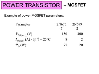
  • 1. – MOSFETPOWER TRANSISTOR Example of power MOSFET parameters; Parameter 2N675 7 2N679 2 VDS(max) (V) 150 400 ID(max) (A) - @ T = 25C 8 2 PD (W) 75 20
  • 2. – MOSFETPOWER TRANSISTOR The superior characteristics of MOSFETs are; • Faster switching time; • No second breakdown; • Stable gain and response time over a wide temperature range (Figure on the next slide).
  • 3. – MOSFETPOWER TRANSISTOR Transconductance versus drain current curves for various values of temperature – less than the variation in BJT current gain.
  • 4. – MOSFETPOWER TRANSISTOR Transfer characteristics curves for various values of temperature.
  • 6. – MOSFETPOWER TRANSISTOR Structure DMOS process can be used to produce a large number of hexagonal cells on a single chip.
  • 7. – MOSFETPOWER TRANSISTOR Structure These hexagonal cells can be paralleled to form large-area devices without the need of emitter ballast resistance. A single power MOSFET may contain as many as 25,000 parallel cells.
  • 8. – MOSFETPOWER TRANSISTOR The “ON” resistive path between drain and source (rds(on)) is an important parameter in power capability of MOSFET
  • 9. – ComparisonPOWER TRANSISTOR BJT Requires complex input circuitry because of high input current (current- controlled device) More sensitive to temperature variation – thermal runaway and problem of second breakdown. MOSFET Simple input circuitry because of low input current (voltage-controlled device). More immune to thermal runaway and second breakdown.
  • 10. – Heat sinksPOWER TRANSISTOR • The power dissipated in a transistor can cause an internal temperature rise above ambient temperature. • This heat, if not properly removed, may cause internal temperature above a safe limit and can cause permanent damage to transistor. • Heat may be removed through proper packaging:
  • 11. – Heat sinksPOWER TRANSISTOR • Additionally, heat sinks can be used to remove the heat developed in the transistor:
  • 12. Heat sinks (Extra)POWER TRANSISTOR Electrical equivalent circuit of thermal- conduction process JADAJ PTT  JT Temperature of transistor junction AT Ambient temperature AJ TT  Temperature difference  Voltage difference JA Thermal resistance between the junction and ambient  Electrical resistance DP Thermal power through the element  Electric current.
  • 13. Heat sinks (Extra)POWER TRANSISTOR Manufacturers’ data sheet for power devices generally give: • maximum operating junction (device) temperature, TJmax; • thermal resistance from the junction to the case, JC; The temperature conduction process may be represented as follows:
  • 14. POWER TRANSISTOR The following equation can be used to describe the temperature conduction process: ambdev TT   amb-snksnkcasecasedev   DP If the heat sink is not used, then;  ambcasecasedevambdev   DPTT Heat sinks (Extra)
  • 15. Heat sinks (Extra)POWER TRANSISTOR A MOSFET has the following parameters; C/W;75.1casedev   Determine the maximum power dissipation in the transistor and determine the temperature of the transistor case and heat sink. EXAMPLE 8.3 C/W;1snk-case   C/W;5amb-snk   C/W;50amb-case   C;150devmax   TTJ C;30amb  T
  • 16. Heat sinks (Extra)POWER TRANSISTOR EXAMPLE 8.3 – Solution Maximum power (without heat sink) W32.2 5075.1 30150 amb-casecase-dev ambmax max         TT P J D Maximum power (with heat sink) amb-snksnk-casecase-dev ambmax max     TT P J D W5.15 5175.1 30150    
  • 17. Heat sinks (Extra)POWER TRANSISTOR EXAMPLE 8.3 – Solution (cont’d) Heat sink temperature amb-snkmaxambsnk DPTT  amb-snkmaxambsnk DPTT  C5.10755.1530  
  • 18. Heat sinks (Extra)POWER TRANSISTOR EXAMPLE 8.3 – Solution (cont’d) Case temperature  amb-snksnk-casemaxambcase   DPTT  amb-snksnk-casemaxambcase   DPTT   C123515.1530   Note: The use of heat sink allows more power to be dissipated in the device.
  • 19. Heat sinks (Extra)POWER TRANSISTOR Power derating curve Manufacturer usually specifies: • the maximum temperature TJmax; • the maximum power dissipation PDmax, at a particular ambient temperature TA0 (usually 25C); and • the thermal resistance JA. In addition, a graph – power derating curve is provided.
  • 20. Heat sinks (Extra)POWER TRANSISTOR Power derating curve For operation below TA0, the device can safely dissipate the rated value of PD0 watts. If the device is to be operated at higher ambient temperature, the maximum allowable power dissipation must be derated according to the straight line.