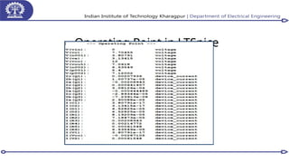
Objectives:
(i) Observe limitationof power efficiency of a CE-CC class A
amplifier
(ii) Design a class-B power amplifier
(iii) Simulate and observe performance of class-B power
amplifier
(iv) Design a class-B push-pull power amplifier (v) Simulate
and observe performance of class-B push-pull power
amplifier
(vi) Design a class-AB push-pull power amplifier (vii)
Simulate and observe performance of class-AB push-pull
power amplifier
3.
(v) Simulate andobserve performance of class-B push-
pull power amplifier
(vi) Design a class-AB push-pull power amplifier
(vii) Simulate and observe performance of class-AB
push-pull power amplifier
Theory
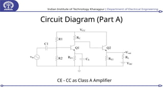
Circuit Description
The ClassA amplifier consists of two cascaded BJTs:
1. Common-Emitter (CE) Stage: The first transistor operates as a voltage amplifier, providing
significant gain.
2. Common-Collector (CC) Stage: The second transistor acts as a buffer, offering impedance matching
and current gain without additional voltage amplification.
The direct coupling of the two stages eliminates the need for inter-stage capacitors, improving the
low-frequency response.
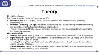
Working Principle
• Biasing: A proper DC biasing network is used to ensure both transistors remain in the active region.
• Signal Flow: The input signal is applied to the base of the first transistor (CE stage), which amplifies
the voltage and inverts the phase.
• Coupling: The amplified signal at the collector of the first transistor directly drives the base of the
second transistor (CC stage).
• Output Characteristics: The CC stage provides a high input impedance and low output impedance,
making it suitable for driving loads efficiently.
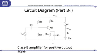
Theory
Operation: Class-B amplifiersare designed to reduce the power dissipation found in
Class-A amplifiers. They achieve this by biasing the transistors at cutoff. This means
that each transistor conducts for only half of the input signal cycle.
Push-Pull Configuration: To reproduce the entire input waveform, Class-B
amplifiers typically use a push-pull configuration. This involves two transistors: one
that conducts for the positive half-cycle and another that conducts for the negative
half-cycle.
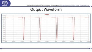
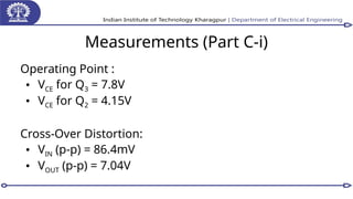
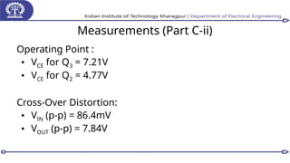
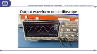
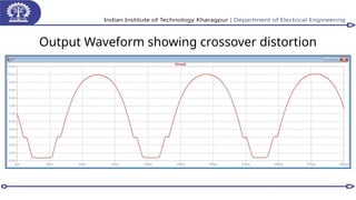
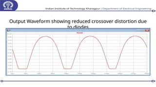
Crossover Distortion: A major drawback of Class-B amplifiers is crossover
distortion. This occurs because neither transistor conducts when the input signal is
near zero, creating a "dead zone" in the output.
15.
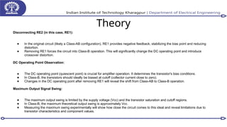
Theory
Disconnecting RE2 (inthis case, RE1):
● In the original circuit (likely a Class-AB configuration), RE1 provides negative feedback, stabilizing the bias point and reducing
distortion.
● Removing RE1 forces the circuit into Class-B operation. This will significantly change the DC operating point and introduce
crossover distortion.
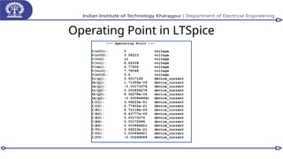
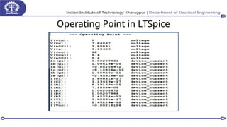
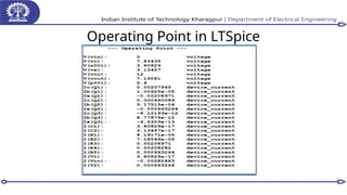
DC Operating Point Observation:
● The DC operating point (quiescent point) is crucial for amplifier operation. It determines the transistor's bias conditions.
● In Class-B, the transistors should ideally be biased at cutoff (collector current close to zero).
● Changes in the DC operating point after removing RE1 will reveal the shift from Class-AB to Class-B operation.
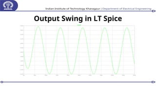
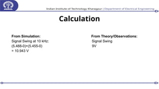
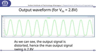
Maximum Output Signal Swing:
● The maximum output swing is limited by the supply voltage (Vcc) and the transistor saturation and cutoff regions.
● In Class-B, the maximum theoretical output swing is approximately Vcc.
● Measuring the maximum swing experimentally will show how close the circuit comes to this ideal and reveal limitations due to
transistor characteristics and component values.
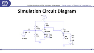
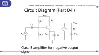
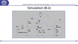
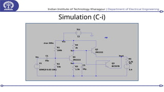
Theory
Negative Output Generation:This circuit utilizes a PNP transistor (Q3) in the output stage,
enabling the generation of a negative voltage swing across the load resistor (RL).
Class-B Operation and Biasing: The aim is for Class-B operation, where Q3 is biased near
cutoff to minimize quiescent power dissipation. The biasing network (R1, R2, RE1) sets the
operating point of Q1, which in turn drives Q3.
Emitter Follower (Q1): Q1 functions as an emitter follower (common-collector amplifier). It
provides a low output impedance to drive the base of Q3, ensuring efficient transfer of the input
signal.
VDC Level Shifting: The VDC source plays a critical role in shifting the DC level of the output
signal. This allows the negative output swing to be centered around a specific voltage,
maximizing the available output range and preventing clipping.
Crossover Distortion: As a Class-B amplifier, this circuit will exhibit crossover distortion. This
occurs due to the "dead zone" around the zero-crossing of the input signal, where neither
transistor is conducting.
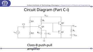
Theory
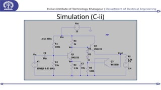
Push-Pull Configuration forFull Waveform: This circuit employs a push-pull configuration, utilizing both an NPN
transistor (Q2) and a PNP transistor (Q3) in the output stage. This design allows for the reproduction of the entire input
waveform, with Q2 handling the positive half-cycle and Q3 handling the negative half-cycle. This effectively mitigates
the crossover distortion inherent in single-transistor Class-B amplifiers.
Class-B Biasing for High Efficiency: Both Q2 and Q3 are biased near cutoff in their quiescent state. This ensures
that minimal power is dissipated when there's no input signal, leading to high power efficiency. Ideally, the theoretical
maximum efficiency of a Class-B amplifier is approximately 78.5%.
Complementary Symmetry Operation: The use of complementary transistors (NPN and PNP) allows for symmetrical
operation. When the input signal goes positive, Q2 turns on and conducts, while Q3 remains off. Conversely, when the
input signal goes negative, Q3 turns on and conducts, while Q2 remains off.
Q1 as a Driver Stage: The NPN transistor Q1 acts as a driver stage. It receives the input signal (Vin) and provides the
necessary current gain and low output impedance to drive both Q2 and Q3 effectively.
VDC for Output Level Adjustment: The VDC source sets the DC level of the output signal. This allows for
symmetrical output swing around a specific voltage, maximizing the available output range and preventing clipping.
Reduced Crossover Distortion: Compared to a single-transistor Class-B amplifier, the push-pull configuration
significantly reduces crossover distortion. The complementary operation of Q2 and Q3 minimizes the "dead zone"
around the zero-crossing of the input signal.
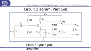
Theory
Class-AB Operation: ReducingCrossover Distortion: This circuit operates in Class-AB mode, a compromise between Class-
A and Class-B. Unlike Class-B, where transistors are biased at cutoff, Class-AB slightly biases Q2 and Q3 to conduct a small
quiescent current. This significantly reduces crossover distortion, the primary drawback of Class-B amplifiers.
Diode Biasing Network (D1, D2): The diodes D1 and D2 are crucial for setting the quiescent current. They provide a voltage
drop that biases the base-emitter junctions of Q2 and Q3 slightly on, eliminating the "dead zone" present in Class-B. The
voltage drop across the diodes defines the quiescent current and minimizes the crossover distortion.
Push-Pull Configuration (Q2, Q3): The circuit utilizes a complementary push-pull configuration with NPN transistor Q2 and
PNP transistor Q3. Q2 conducts during the positive half-cycle of the input signal, while Q3 conducts during the negative half-
cycle, enabling the reproduction of the full waveform.
Q1 as a Driver Stage: The NPN transistor Q1 acts as a driver stage, providing the necessary current gain and low output
impedance to efficiently drive the bases of Q2 and Q3. This ensures that the output stage receives a strong signal to accurately
reproduce the input.
VDC for Output Level Adjustment: The VDC source sets the DC level of the output signal. This allows for a symmetrical
output swing around a specific voltage, maximizing the available output range and preventing clipping.
RD for Bias Stabilization and Current Limiting: The resistor RD is used to stabilize the bias point of the output stage and limit
the current through the diodes and transistors. It helps prevent thermal runaway and ensures stable operation.
Efficiency Considerations: While Class-AB amplifiers offer better linearity than Class-B, they have slightly lower efficiency due
to the quiescent current. However, their efficiency is still significantly higher than Class-A amplifiers.
Key Takeaways
Efficiency Limitationsof Class A Amplifiers – The experiment highlights that Class A amplifiers suffer from
low power efficiency due to continuous transistor conduction, leading to high power dissipation. This makes
them unsuitable for high-power applications despite their superior signal fidelity.
Class B Amplifier Performance – By designing and simulating a Class B amplifier, the experiment
demonstrates improved efficiency by using transistors that conduct only for half the input signal cycle, reducing
power wastage. However, this improvement comes at the cost of potential signal distortion at low input levels.
Crossover Distortion in Class B Amplifiers – A significant drawback of Class B amplifiers is crossover
distortion at the zero-crossing point of the signal, which affects output signal quality. This occurs due to a brief
period when neither transistor is conducting, leading to a gap in the output waveform.
Class AB Push-Pull Amplifier for Distortion Reduction – To minimize crossover distortion, a Class AB push-
pull amplifier is designed, which slightly biased transistors into conduction, ensuring smoother transitions and
better performance. This compromise allows for a balance between efficiency and signal fidelity, making it a
common choice for audio applications.
44.
Conclusion
This experiment providedvaluable insights into the working principles and trade-offs associated with
different classes of amplifiers—Class A, Class B, and Class AB. Through circuit design, simulation, and
analysis, we observed that while Class A amplifiers offer excellent linearity and minimal distortion,
they are highly inefficient due to continuous transistor conduction, leading to excessive power
dissipation.
In contrast, Class B amplifiers significantly improve efficiency by operating transistors in a push-pull
manner, where each transistor conducts only for half the input cycle. However, this results in
crossover distortion at the zero-crossing point, which negatively impacts signal quality, especially in
low-power applications. To overcome this limitation, Class AB amplifiers introduce a small biasing
voltage that keeps both transistors slightly conducting, thereby reducing distortion while still
maintaining relatively high efficiency.
The experiment highlights the importance of selecting the appropriate amplifier class based on
application needs. While Class A amplifiers are preferred in high-fidelity audio applications due to
their superior signal reproduction, Class B and AB configurations are more suitable for power-
efficient applications such as audio amplification in consumer electronics and radio transmission.
The findings reinforce the necessity of balancing efficiency, power dissipation, and signal fidelity in


![July07 4[1].1 power_amplifiers01](https://cdn.slidesharecdn.com/ss_thumbnails/july0741-200727121307-thumbnail.jpg?width=640&height=640&fit=bounds)