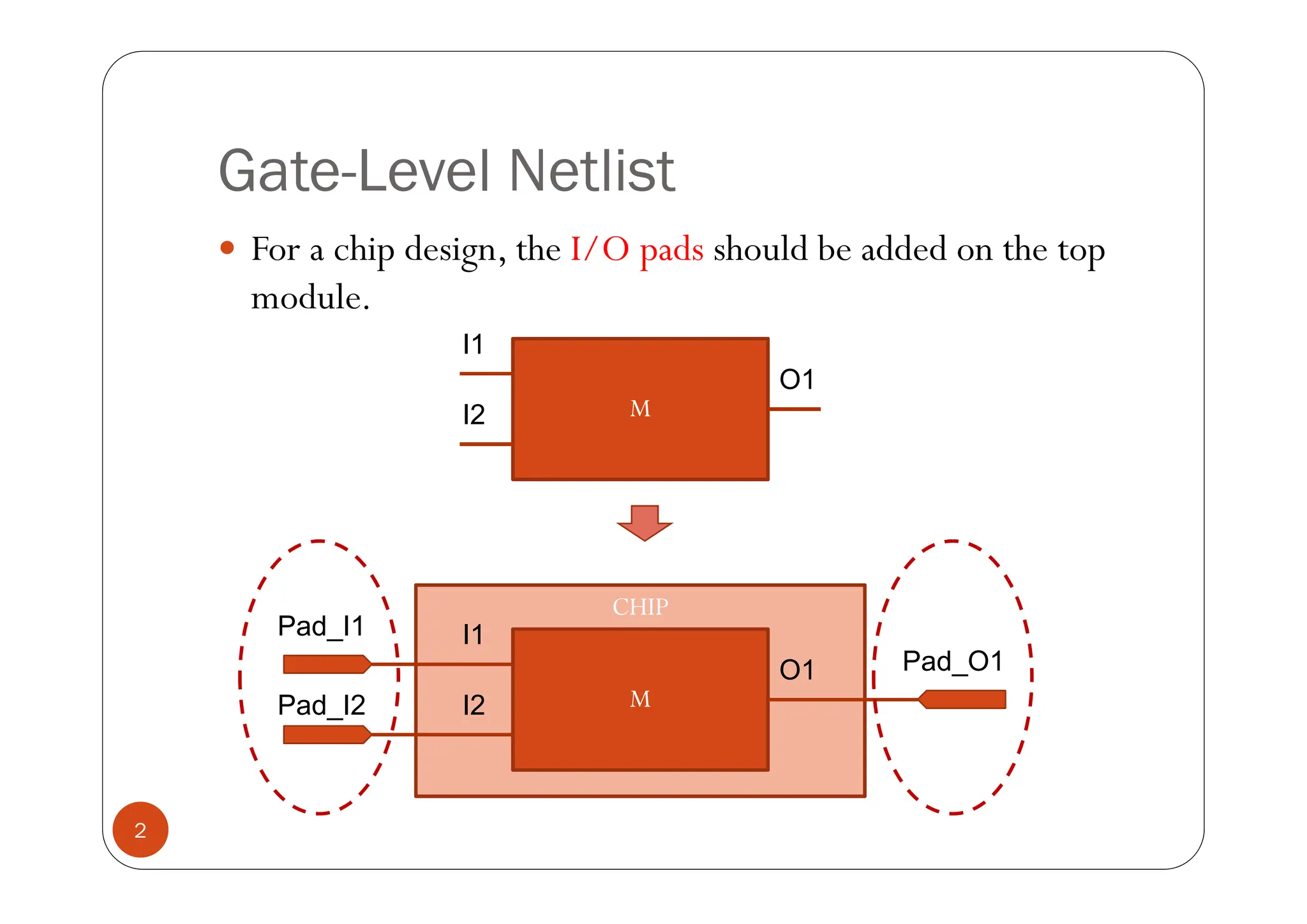
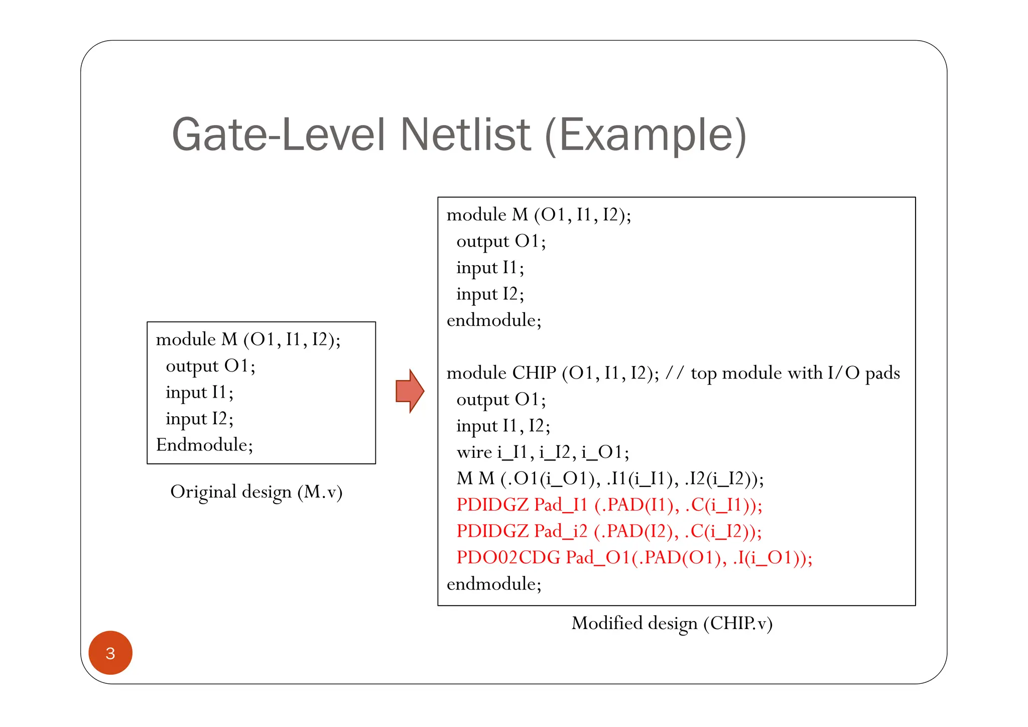
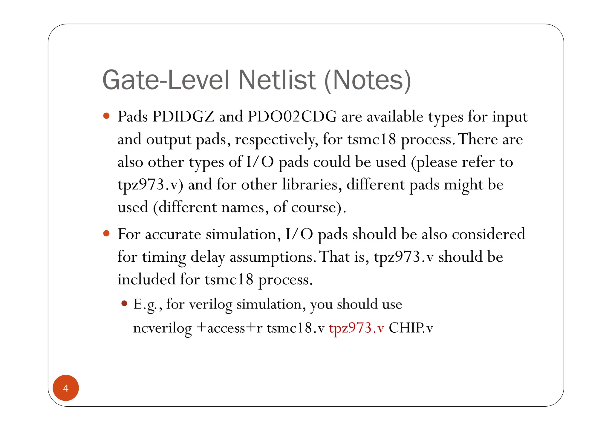
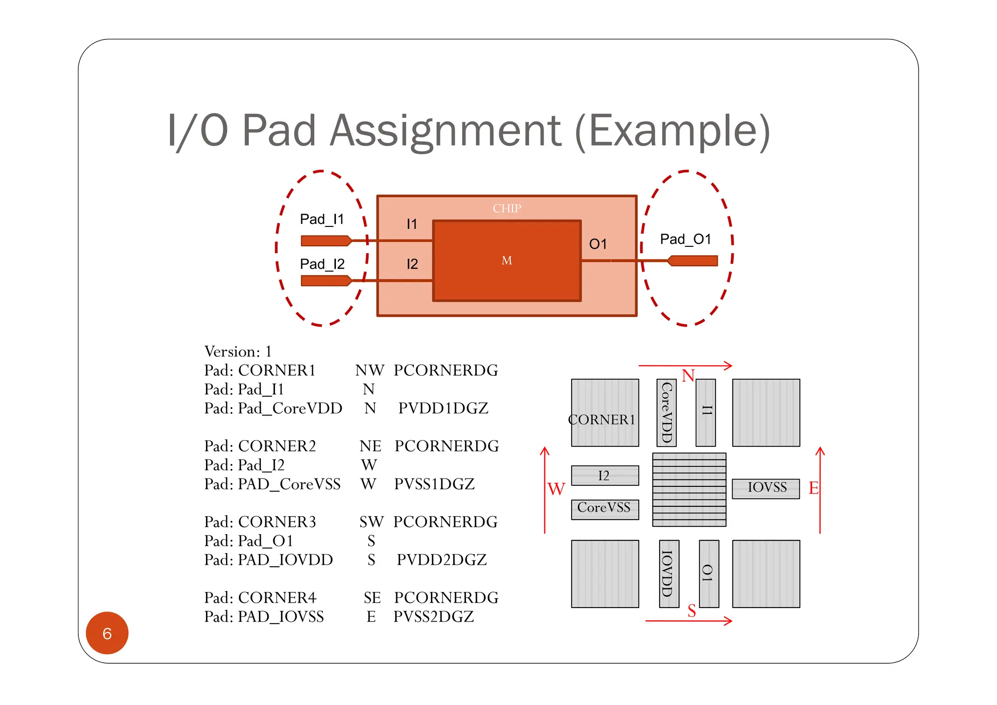
I/O Pad Insertion for Cadence Innovus
Ahmed Abdelazeem
Gate-Level Netlist
 For a chip design the I/O pads should be added on the top
 For a chip design, the I/O pads should be added on the top
module.
I1
M
I2
O1
CHIP
I1
O1
Pad_I1
Pad O1
M
I2
O1
Pad_I2
_
2
Gate-Level Netlist (Example)
module M (O1, I1, I2);
output O1;
input I1;
input I2;
endmodule;
module M (O1, I1, I2);
t t O1 module CHIP (O1, I1, I2); // top module with I/O pads
output O1;
input I1, I2;
i i I1 i I2 i O1
output O1;
input I1;
input I2;
Endmodule; wire i_I1, i_I2, i_O1;
M M (.O1(i_O1), .I1(i_I1), .I2(i_I2));
PDIDGZ Pad_I1 (.PAD(I1), .C(i_I1));
PDIDGZ P d i2 ( PAD(I2) C(i I2))
Endmodule;
Original design (M.v)
PDIDGZ Pad_i2 (.PAD(I2), .C(i_I2));
PDO02CDG Pad_O1(.PAD(O1), .I(i_O1));
endmodule;
3
Modified design (CHIP.v)
Gate-Level Netlist (Notes)
 Pads PDIDGZ and PDO02CDG are available types for input
and output pads, respectively, for tsmc18 process.There are
also other types of I/O pads could be used (please refer to
a so ot e types o /O pa s cou e use (p ease e e to
tpz973.v) and for other libraries, different pads might be
used (different names, of course).
( )
 For accurate simulation, I/O pads should be also considered
for timing delay assumptions.That is, tpz973.v should be
g y p , p
included for tsmc18 process.
 E.g., for verilog simulation, you should use
g g
ncverilog +access+r tsmc18.v tpz973.v CHIP.v
4
I/O Pad Assignment
 You should write ioc file according to your design before
 You should write .ioc file according to your design before
P&R.
 In v file if no power pad information is included you may
 In .v file, if no power pad information is included, you may
add a new power pad by yourself.
 VDD: PVDD1DGZ PVDD2DGZ // tsmc18 library
VDD: PVDD1DGZ, PVDD2DGZ // tsmc18 library
 VSS: PVSS1DGZ, PVSS2DGZ // tsmc18 library
 Note: there are two types of power pads: (1) power pads for the
Note: there are two types of power pads: (1) power pads for the
core (design), (2) power pads for I/O pads
 Corner pads
p
 PCORNERDG // tsmc18 library
 For other pads (design inputs/outputs), you should arrange
For other pads (design inputs/outputs), you should arrange
them by yourself.
5
I/O Pad Assignment (Example)
CHIP
M
I1
I2
O1
Pad_I1
Pad_I2
Pad_O1
Version: 1
Version: 1
Pad: CORNER1 NW PCORNERDG
Pad: Pad_I1 N
Pad: Pad_CoreVDD N PVDD1DGZ
CORNER1
I1
CoreVD
N
Pad: CORNER2 NE PCORNERDG
Pad: Pad_I2 W
Pad: PAD_CoreVSS W PVSS1DGZ I2
CoreVSS
IOVSS
D
E
W
Pad: CORNER3 SW PCORNERDG
Pad: Pad_O1 S
Pad: PAD_IOVDD S PVDD2DGZ
P d CORNER4 SE PCORNERDG
IOVDD
O1
6
Pad: CORNER4 SE PCORNERDG
Pad: PAD_IOVSS E PVSS2DGZ
D
S
I/O Pad Assignment (Notes)
 For correct P&R you should make sure that in the v file
 For correct P&R, you should make sure that in the .v file
(CHIP.v), I/O pads are correctly connected to your original
design without pads.
es g w t out pa s.
 For power and corner pads (which are not included in the .v
file), pad types should be specified in the .ioc file.
 Pads are not necessarily uniformly distributed. (That is, we
can have different numbers of pads in different directions)
However, uniform assignment is suggested.
 You might use more than one set of power pads (E g
You might use more than one set of power pads (E.g.,
IOVDD1, IOVDD2, CoreVDD1, CoreVDD2).
 Different rearrangements will result in different placement
Different rearrangements will result in different placement,
routing, timing, power, etc.
7

IO Pad Insertion.pdf

  • 1.
    I/O Pad Insertionfor Cadence Innovus Ahmed Abdelazeem
  • 2.
    Gate-Level Netlist  Fora chip design the I/O pads should be added on the top  For a chip design, the I/O pads should be added on the top module. I1 M I2 O1 CHIP I1 O1 Pad_I1 Pad O1 M I2 O1 Pad_I2 _ 2
  • 3.
    Gate-Level Netlist (Example) moduleM (O1, I1, I2); output O1; input I1; input I2; endmodule; module M (O1, I1, I2); t t O1 module CHIP (O1, I1, I2); // top module with I/O pads output O1; input I1, I2; i i I1 i I2 i O1 output O1; input I1; input I2; Endmodule; wire i_I1, i_I2, i_O1; M M (.O1(i_O1), .I1(i_I1), .I2(i_I2)); PDIDGZ Pad_I1 (.PAD(I1), .C(i_I1)); PDIDGZ P d i2 ( PAD(I2) C(i I2)) Endmodule; Original design (M.v) PDIDGZ Pad_i2 (.PAD(I2), .C(i_I2)); PDO02CDG Pad_O1(.PAD(O1), .I(i_O1)); endmodule; 3 Modified design (CHIP.v)
  • 4.
    Gate-Level Netlist (Notes) Pads PDIDGZ and PDO02CDG are available types for input  Pads PDIDGZ and PDO02CDG are available types for input and output pads, respectively, for tsmc18 process.There are also other types of I/O pads could be used (please refer to a so ot e types o /O pa s cou e use (p ease e e to tpz973.v) and for other libraries, different pads might be used (different names, of course). ( )  For accurate simulation, I/O pads should be also considered for timing delay assumptions.That is, tpz973.v should be g y p , p included for tsmc18 process.  E.g., for verilog simulation, you should use g g ncverilog +access+r tsmc18.v tpz973.v CHIP.v 4
  • 5.
    I/O Pad Assignment You should write ioc file according to your design before  You should write .ioc file according to your design before P&R.  In v file if no power pad information is included you may  In .v file, if no power pad information is included, you may add a new power pad by yourself.  VDD: PVDD1DGZ PVDD2DGZ // tsmc18 library VDD: PVDD1DGZ, PVDD2DGZ // tsmc18 library  VSS: PVSS1DGZ, PVSS2DGZ // tsmc18 library  Note: there are two types of power pads: (1) power pads for the Note: there are two types of power pads: (1) power pads for the core (design), (2) power pads for I/O pads  Corner pads p  PCORNERDG // tsmc18 library  For other pads (design inputs/outputs), you should arrange For other pads (design inputs/outputs), you should arrange them by yourself. 5
  • 6.
    I/O Pad Assignment(Example) CHIP M I1 I2 O1 Pad_I1 Pad_I2 Pad_O1 Version: 1 Version: 1 Pad: CORNER1 NW PCORNERDG Pad: Pad_I1 N Pad: Pad_CoreVDD N PVDD1DGZ CORNER1 I1 CoreVD N Pad: CORNER2 NE PCORNERDG Pad: Pad_I2 W Pad: PAD_CoreVSS W PVSS1DGZ I2 CoreVSS IOVSS D E W Pad: CORNER3 SW PCORNERDG Pad: Pad_O1 S Pad: PAD_IOVDD S PVDD2DGZ P d CORNER4 SE PCORNERDG IOVDD O1 6 Pad: CORNER4 SE PCORNERDG Pad: PAD_IOVSS E PVSS2DGZ D S
  • 7.
    I/O Pad Assignment(Notes)  For correct P&R you should make sure that in the v file  For correct P&R, you should make sure that in the .v file (CHIP.v), I/O pads are correctly connected to your original design without pads. es g w t out pa s.  For power and corner pads (which are not included in the .v file), pad types should be specified in the .ioc file. file), pad types should be specified in the .ioc file.  Pads are not necessarily uniformly distributed. (That is, we can have different numbers of pads in different directions) can have different numbers of pads in different directions) However, uniform assignment is suggested.  You might use more than one set of power pads (E g You might use more than one set of power pads (E.g., IOVDD1, IOVDD2, CoreVDD1, CoreVDD2).  Different rearrangements will result in different placement Different rearrangements will result in different placement, routing, timing, power, etc. 7