Static timing analysis (STA) is a method of validating the timing performance of a design by checking all possible paths for timing violations. STA breaks a design down into timing paths, calculates the signal propagation delay along each path, and checks for violations of timing constraints inside the design and at the input/output interface.


![Ahmed Abdelazeem
Ahmed Abdelazeem
Topic 11: report timing paths
report_timing -net -input -tran –cap –derate –voltage –crosstalk –max_paths –nworst
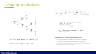
➢ -net not only shows the net between pin nodes, but also show the number of fanouts for each net
➢ -input shows the input pin through which the path is going through. It’s useful when tracing report through multiple input cells. Also, it split the delay associate to a cell into net
delay and cell delay.
➢ -tran shows both the input and output transition time used for or calculated by the delay calculation.
➢ -cap shows the total capacitance appear on the net, including both wire capacitance and input pin cap from next stage
➢ -derate show the derating factor used for the delay value.
➢ -voltage show the operating voltage set to do the analysis, useful when the design involves multiple power domain and rail voltage.
➢ -crosstalk show the delta delay calculated during signal integrity check or manually annotated.
➢ -max_path show the maximum total paths to be reported among all path groups. –nworst shows the maximum number of paths to be reported for a single endpoint
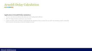
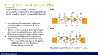
report_timing –pba_mode [none | path | exhaustive]
In addition to all the switches above, -pba_mode enables the pba mode reporting
➢ none (the default) - Path-based analysis is not applied.
➢ path - Path-based analysis is applied to paths after they have been gathered.
➢ exhaustive - An exhaustive path-based analysis path search algorithm is applied to
determine the worst path-based analysis path set in the design.
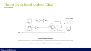
update_timing
If the timing constraints have been changed, STA engine will need to re-calculate the
timing graph again. Even though report_timing will re-time the design implicitly
(incrementally), It’s always a good practice to do an explicit update_timing explicitly
before report_timing.
By default, the update_timing command uses an efficient timing analysis algorithm that
requires minimal computation effort and updates existing timing analysis information
only where needed. You can override this default behavior using the -full option, which
causes the entire timing update to be performed from the beginning.](https://image.slidesharecdn.com/delaycalculation-250530192911-03116e20/85/Back2School-Delay-Calculation-Chapter-2-84-320.jpg)


![[Back2School] Constraint Develop.pdf- Chapter 3](https://cdn.slidesharecdn.com/ss_thumbnails/constraintdevelop-250606153235-d8296a49-thumbnail.jpg?width=640&height=640&fit=bounds)
![[Back2School] STA Basic Concepts- Chapter 1.pdf](https://cdn.slidesharecdn.com/ss_thumbnails/stabasicconcepts-250524204554-25ac4895-thumbnail.jpg?width=640&height=640&fit=bounds)

![[Back2School] Timing Checks- Chapter 5.pdf](https://cdn.slidesharecdn.com/ss_thumbnails/specialtimingchecks-250609185635-cf7ed43c-thumbnail.jpg?width=640&height=640&fit=bounds)
![[Back2School] STA Methodology- Chapter 7pdf](https://cdn.slidesharecdn.com/ss_thumbnails/stamethodology-250624214856-5fd24ebc-thumbnail.jpg?width=640&height=640&fit=bounds)


![[Back2School] Timing Verification- Chapter 4](https://cdn.slidesharecdn.com/ss_thumbnails/timingverification-250607212312-4e8e2612-thumbnail.jpg?width=640&height=640&fit=bounds)


![[Back2School] Crosstalk and Noise- Chapter 6.pdf](https://cdn.slidesharecdn.com/ss_thumbnails/crosstalkandnoise-250624214313-69c347be-thumbnail.jpg?width=640&height=640&fit=bounds)