1-2
Agenda
Course Description
Book, Labs,Equipment
Grading Criteria
Expectations/Responsibilities
Prerequisites
Embedded Systems
Microcontrollers
Product Life Cycle
Analysis, Design, Implementation, Testing
Flowcharts, Data-Flow and Call Graphs
ARM Architecture
Programming
Integrated Development Environment (IDE)
3.
1-3
Useful Info
• Nolabs this week!
• Lab lectures start this Friday
• F 4–5, M 6:30–7:30 and 7:30-8:30 (ECJ 1.202)
• Office hours: see Canvas for most recent?
• TAs have office hours too
• They are not there to do your work for you
• One course == common exams and HW
• 2/23 7–8:30 (15%) 4/6 7–8:30 (20%) Final TBD (25%)
• Most of the learning is in the labs
• 10 labs 30% of grade
• HW is important too so 10% for motivation
• Read the book and lab manual!
• Canvas, Piazza, and
users.ece.utexas.edu/~valvano/Volume1/
4.
1-4
Action Items
• Comeintroduce yourselves
• Take stock of resources
• Class Website (Volume1)
• Piazza for class discussions
• Email to reach TAs+Me
• E-Book: Search “Valvano e-book”
• Order board
• Install SW
• Read Chapters 1 & 2 of book
5.
1-5
DOs and DON’Ts
DO
•Read
•Book, lab, datasheets
•Try before seeking help
•Follow Piazza/Canvas
•Discuss material with
others
•Homework (not labs) in
groups
•Consult the web
•Track due dates
DON’T
•Don’t cheat!
•Never look at another
student’s code (current
or previous)
•Don’t let your partner do
all the work
•Don’t copy software from
book or web without
attribution
•Don’t expect handholding
6.
1-6
EE306 Recap: DigitalLogic
Positive logic: Negative logic :
True is higher voltage True is lower voltage
False is lower voltage False is higher voltage
AND, OR, NOT
Flip flops
Registers
A ~A
74HC04
+3.3V
~A
n-type
p-type source
gate
A
drain
drain
gate source
0 V active off +3.3V
+3.3V off active 0V
A p-type n-type ~A
A
0
1
~A
1
0
1-8
EE302 Recap: Ohm’sLaw
V = I * R Voltage = Current * Resistance
I = V / R Current = Voltage / Resistance
R = V / I Resistance = Voltage / Current
R = 1k
Battery
V=3.7V
Resistor
I = 3.7mA
R
I
V
•P = V * I Power = Voltage * Current
•P = V2
/ R Power = Voltage2
/ Resistance
•P = I2
* R Power = Current2
* Resistance
1 amp is 6.241×10¹⁸
electrons per second =
1 coulomb/sec
9.
1-9
Embedded System
EmbeddedSystems are
everywhere
Ubiquitous, invisible
Hidden (computer inside)
Dedicated purpose
Microprocessor
Intel: 4004, ..8080,.. x86
Freescale: 6800, ..
9S12,.. PowerPC
ARM, DEC, SPARC, MIPS,
PowerPC, Natl. Semi.,…
Microcontroller
Processor+Memory+
I/O Ports (Interfaces)
I/O Ports
Microcontroller Electrical,
mechanical,
chemical,
or
optical
devices
Embedded system
Bus ADC
Analog
signals
LM3S or TM4C
DAC
Processor
RAM
ROM
Medical
Automotive
Communications
Comsumer Industrial
Military
10.
1-10
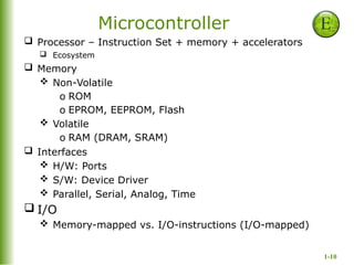
Microcontroller
Processor –Instruction Set + memory + accelerators
Ecosystem
Memory
Non-Volatile
o ROM
o EPROM, EEPROM, Flash
Volatile
o RAM (DRAM, SRAM)
Interfaces
H/W: Ports
S/W: Device Driver
Parallel, Serial, Analog, Time
I/O
Memory-mapped vs. I/O-instructions (I/O-mapped)
11.
1-11
Texas Instruments TM4C123
ARMCortex-M4
+ 256K EEPROM
+ 32K RAM
+ JTAG
+ Ports
+ SysTick
+ ADC
+ UART
GPIO Port D
GPIO Port A
ADC
2 channels
12 inputs
12 bits
PA7
PA6
PA5/SSI0Tx
PA4/SSI0Rx
PA3/SSI0Fss
PA2/SSI0Clk
PA1/U0Tx
PA0/U0Rx
PC7
PC6
PC5
PC4
PC3/TDO/SWO
PC2/TDI
PC1/TMS/SWDIO
PC0/TCK/SWCLK
PE5
PE4
PE3
PE2
PE1
PE0
GPIO Port C
GPIO Port E
JTAG
Four
SSIs
Eight
UARTs
PB7
PB6
PB5
PB4
PB3/I2C0SDA
PB2/I2C0SCL
PB1
PB0
PD7
PD6
PD5
PD4
PD3
PD2
PD1
PD0
PF4
PF3
PF2
PF1
PF0
GPIO Port B
Four
I2Cs
USB 2.0
Cortex M4 Systick
NVIC
Two Analog
Comparators
Advanced Peripheral Bus
Twelve
Timers
Six
64-bit wide
CAN 2.0
System Bus Interface
GPIO Port F
Advanced High Performance Bus
Two PWM
Modules
12.
1-12
LaunchPad Switches andLEDs
TM4C123 PF0
PF4
R1 0
SW1 SW2
PF3
PF2
PF1
330
Red
330
Blue
5V
330
Green
DTC114EET1G
PD0
PB6
PD1
PB7
0
R9
0
R10
0
R12
0
R11
0
R2
R13 0
PA1
PA0
PD5
PD4
Serial
USB
PB1
R29
0
R25
PB0
+5
0
The switches on the LaunchPad
Negative logic
Require internal pull-up (set bits in PUR)
The PF3-1 LEDs are positive logic
13.
1-13
I/O Ports andControl Registers
The input/output direction of a bidirectional port is
specified by its direction register.
GPIO_PORTF_DIR_R , specify if corresponding
pin is input or output:
0 means input
1 means output
Input/Output Port
D Q
Write to port direction register
Direction bits
D Q
Write to port address
Processor
Read from port address
Bus
n
n
n
n
n 1 means output
0 means input
GPIO_PORTF_DATA_R
GPIO_PORTF_DIR_R
14.
1-14
I/O Ports andControl Registers
Address 7 6 5 4 3 2 1 0 Name
400F.E608 - - GPIOF GPIOE GPIOD GPIOC GPIOB GPIOA SYSCTL_RCGCGPIO_R
4002.53FC - - - DATA DATA DATA DATA DATA GPIO_PORTF_DATA_R
4002.5400 - - - DIR DIR DIR DIR DIR GPIO_PORTF_DIR_R
4002.5420 - - - SEL SEL SEL SEL SEL GPIO_PORTF_AFSEL_R
4002.551C - - - DEN DEN DEN DEN DEN GPIO_PORTF_DEN_R
• Initialization (executed once at beginning)
1. Turn on clock in SYSCTL_RCGCGPIO_R
2. Wait two bus cycles (two NOP instructions)
3. Unlock PF0 (PD7 also needs unlocking)
4. Set DIR to 1 for output or 0 for input
5. Clear AFSEL bits to 0 to select regular I/O
6. Set PUE bits to 1 to enable internal pull-up
7. Set DEN bits to 1 to enable data pins
• Input/output from pin
6. Read/write GPIO_PORTF_DATA_R
15.
1-15
Done
• Hardware
• Software
•Specifications
• Constraints
Analyze
the
problem
Requirements
Design
Constraints
Testing
• Block diagrams
• Data flow graphs
Deployment
New requirements
New constraints
Development
Product Life Cycle
Analysis (What?)
Requirements ->
Specifications
Design (How?)
High-Level: Block Diagrams
Engineering: Algorithms,
Data Structures, Interfacing
Implementation(Real)
Hardware, Software
Testing (Works?)
Validation:Correctness
Performance: Efficiency
Maintenance (Improve)
16.
1-16
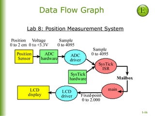
Data Flow Graph
Lab8: Position Measurement System
Position
Sensor
Voltage
0 to +3.3V
ADC
hardware
ADC
driver
Sample
0 to 4095
SysTick
ISR
Sample
0 to 4095
SysTick
hardware
LCD
display
LCD
driver Fixed-point
0 to 2.000
Position
0 to 2 cm
main
Mailbox
1-18
Structured Programming
Common Constructs(as Flowcharts)
Fork
Join
Trigger
interrupt
Return from
interrupt
main1
Init1
Body1
main2
Init2
Body2
main
Init
Body
Parallel Distributed Interrupt-driven concurrent
Block 1
Sequence Conditional While-loop
Block 2
Block 1 Block 2 Block
19.
1-19
Flowchart
Toaster oven:
Coding inassembly and/or high-level language (C)
main
toast < desired
Output heat
is on Too cold
Input from
switch
Input toast
temperature
toast desired
Start
Not pressed
Pressed
Output heat
is off
Cook
return
Cook
20.
1-20
Flowchart
Example 1.3.Design a flowchart for a system that performs two independent
tasks. The first task is to output a 20 kHz square wave on PORTA in real time
(period is 50 ms). The second task is to read a value from PORTB, divide the value
by 4, add 12, and output the result on PORTD. This second task is repeated over
and over.
Clock
void SysTick_Handler(void){
PORTA = PORTA^0x01;
}
E
E
<
>
>
void main(void){
unsigned long n;
while(1){
n = PORTB;
n = (n/4)+12;
PORTD = n;
}
}
B
C
D
A
main
Input n from
PORTB
A
B
D
C
n = (n/4)+12
Output n to
PORTD
PORTA =
PORTA^1
21.
1-21
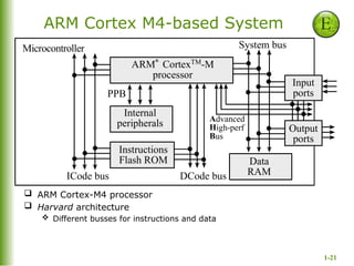
ARM Cortex M4-basedSystem
DCode bus
ARM® CortexTM
-M
processor
Data
RAM
Instructions
Flash ROM
Input
ports
Output
ports
Microcontroller
ICode bus
Internal
peripherals
PPB
System bus
Advanced
High-perf
Bus
ARM Cortex-M4 processor
Harvard architecture
Different busses for instructions and data
22.
1-22
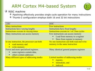
ARM Cortex M4-basedSystem
RISC machine
Pipelining effectively provides single cycle operation for many instructions
Thumb-2 configuration employs both 16 and 32 bit instructions
CISC RISC
Many instructions Few instructions
Instructions have varying lengths Instructions have fixed lengths
Instructions execute in varying times Instructions execute in 1 or 2 bus cycles
Many instructions can access memory Few instructions can access memory
Load from memory to a register
Store from register to memory
In one instruction, the processor can both
read memory and
write memory
No one instruction can both read and write
memory in the same instruction
Fewer and more specialized registers.
some registers contain data,
others contain addresses
Many identical general purpose registers
Many different types of addressing modes Limited number of addressing modes
register,
immediate, and
indexed.
23.
1-23
ARM ISA: Thumb2Instruction Set
Variable-length instructions
ARM instructions are a fixed
length of 32 bits
Thumb instructions are a fixed
length of 16 bits
Thumb-2 instructions can be
either 16-bit or 32-bit
Thumb-2 gives approximately 26%
improvement in code density over
ARM
Thumb-2 gives approximately 25%
improvement in performance over
Thumb
24.
1-24
ARM ISA: Registers,Memory-map
R0
R1
R2
R3
R4
R5
R6
R7
R8
R9
R10
R11
R12
R13 (MSP)
R14 (LR)
R15 (PC)
Stack pointer
Link register
Program counter
General
purpose
registers
TI TM4C123
Microcontroller
256k Flash
ROM
32k RAM
I/O ports
Internal I/O
PPB
0x0000.0000
0x0003.FFFF
0x2000.0000
0x2000.7FFF
0x4000.0000
0x400F.FFFF
0xE000.0000
0xE004.1FFF
Condition Code Bits Indicates
N negative Result is negative
Z zero Result is zero
V overflow Signed overflow
C carry Unsigned overflow
25.
1-25
LC3 to ARM- Data Movement
LEA R0, Label ;R0 <- PC + Offset to Label
ADR R0,Label or LDR R0,=Label
LD R1,Label ; R1 <- M[PC + Offset]
LDR R0,=Label ; Two steps: (i) Get address into R0
LDRH R1,[R0] ; (ii) Get content of address [R0] into R1
LDR R1,R0,n ; R1 <- M[R0+n]
LDRH R1,[R0,#n]
LDI R1,Label ; R1 <- M[M[PC + Offset]]
; Three steps!!
ST R1,Label ; R1 -> M[PC + Offset]
LDR R0,=Label ; Two steps: (i)Get address into R0
STRH R1,[R0] ; (ii) Put R1 contents into address in R0
STR R1,R0,n ; R1 -> M[R0+n]
STRH R1,[R0,#n]
STI R1,Label ; R1 -> M[M[PC + Offset]]
; Three steps!!
26.
1-26
LC3 to ARM– Arithmetic/Logic
ADD R1, R2, R3 ; R1 <- R2 + R3
ADD R1,R2,R3 ; 32-bit only
ADD R1,R2,#5 ; R1 <- R2 + 5
ADD R1,R2,#5 ; 32-bit only, Immediate is 12-bit
AND R1,R2,R3 ; R1 <- R2 & R3
AND R1, R2, R3 ; 32-bit only
AND R1,R2,#1 ; R1 <- Bit 0 of R2
AND R1, R2, #1 ; 32-bit only
NOT R1,R2 ; R1 -> ~(R2)
EOR R1,R2,#-1 ; -1 is 0xFFFFFFFF,
; so bit XOR with 1 gives
complement
27.
1-27
LC3 to ARM– Control
BR Target ; PC <- Address of Target
B Target
BRnzp Target ; PC <- Address of Target
B Target
BRn Target ; PC <- Address of Target if N=1
BMI Target ; Branch on Minus
BRz Target ; PC <- Address of Target if Z=1
BEQ Target
BRp Target ; PC <- Address of Target if P=1
No Equivalent
BRnp Target ; PC <- Address of Target if Z=0
BNE Target
BRzp Target ; PC <- Address of Target if N=0
BPL Target ; Branch on positive or zero (Plus)
BRnz Target ; PC <- Address of Target if P=0
No Equivalent
28.
1-28
LC3 to ARM– Subs,TRAP,Interrupt
JSR Sub ; PC <- Address of Sub, Return address in R7
BL Sub ; PC<-Address of Sub, Ret. Addr in R14 (Link Reg)
JSRR R4 ; PC <- R4, Return address in R7
BLX R4 ; PC <-R4, Return address in R14 (Link Reg)
RET ; PC <- R7 (Implicit JMP to address in R7)
BX LR ; PC <- R14 (Link Reg)
JMP R2 ; PC <- R2
BX R2 ; PC <- R14 (Link Reg)
TRAP x25 ; PC <- M[x0025], Return address in R7
SVC #0x25 ; Similar in concept but not implementation
RTI ; Pop PC and PSR from Supervisor Stack…
BX LR ; PC <- R14 (Link Reg) [same as RET]
29.
1-29
ARM is aLoad-Store machine
Code to set (to 1) bit 5 of memory address x400FE608
SYSCTL_RCGCGPIO_R EQU 0x400FE608
; EQU psedo-op allows use of
; symbolic name to represent a constant
LDR R1, =SYSCTL_RCGCGPIO_R ; R1 holds x400FE608
LDR R0, [R1] ; R0 holds contents of
; location x400FE608
ORR R0, R0, #0x20 ; bit5 of R0 is set to 1
STR R0, [R1] ; write R0 contents back to
; location x400FE608
#1 Great class, combines concepts, skills, and experience.
Build real systems, bridge physical and virtual. Embedded systems critical to everyone, knowledge gained goes way beyond that.
Learn to how a system works and development flow, learn how a computer and embedded system works practically, learn how to program, learn how to use programming tools and mixed environments, learn about interfacing and design
#2 To do this week: get book, order a board, {read chapters 1 and 2 of the book or ebook 2 3 4}, do ws01, do HW1, install Keil uVision 4.73 on laptop
#9 Consumer electronics: Washing machine, Exercise equipment, Remote controls, Clocks and watches, Games and toys, Audio/video electronics, Set-back thermostats, Camera, Camcorder, Television, VCR, cable box
Communication systems: Answering machines, Telephones, Fax machines, Radios, Cellular phones, pagers
Automotive systems: Automatic breaking, Noise cancellation, Locks, Electronic ignition, Power windows and seats, Cruise control, Collision avoidance, Climate control, Emission control, Instrumentation
Military hardware: Smart weapons, Missile guidance systems, Global positioning systems, Surveillance systems
Business applications: Cash registers, Vending machines, ATM machines, Traffic controllers, Industrial robots, Bar code readers and writers, Automatic sprinklers, Elevator controllers, RFID systems, Lighting and heating systems
Medical devices: Monitors, Drug delivery systems, Cancer treatments, Pacemakers, Prosthetic devices, Dialysis machines
#10 Processor
There are two classifications of computers: complex instruction set computer (CISC) and reduced instruction set computer (RISC). In reality, there is a spectrum of architectures that we can classify as CISC or RISC. We make these general observations when deciding whether to call a computer CISC or RISC:
Complex instruction set computers (CISC)
Early computers offered CPUs that were much faster than available memories.
Fetching instructions limited performance
A single complex instruction could perform many operations
Example: Find the zeros of a polynomial
Complex instructions require many processor clock cycles to complete and most instructions can access memory
A program running on a CISC computer employed a relatively small number of complex instructions
High code density, many instruction types w/ varying length, fewer and specialized registers, many addressing modes
Complexity is embedded in the processor hardware (overhead)
Examples: Intel (x86), Freescale 9S12
Reduced Instruction Set Computers (RISC)
Memories match CPU speed
No large penalty for instruction fetch
Instructions simplified
Example: dedicated load/store instructions, regular instructions can not access memory but only registers
Single processor clock cycle per instruction (pipelined)
A program running on a RISC computer employs a relatively larger number of simplified instructions
Reduced code density, few instructions w/ fixed delay (pipeline!), many identical general-purpose registers, few addressing modes
Complexity exists in the assembly code generated by the programmer or compiler, hardware is simple (low overhead/low power)
Examples: LC3, MIPS, ARM, SPARC, PowerPC
Which architecture is best is beyond the scope of this class, but it is important to recognize the terminology. It is very difficult to compare the execution speed of two computers, especially between a CISC and a RISC. One way to compare is to run a benchmark program on both, and measure the time it takes to execute.
Time to execute benchmark = Instructions/program * Average cycles/instruction * Seconds/cycle For example, the 50 MHz ARM Cortex M has one bus cycle every 20ns. One average it may require 1.5 cycles per instruction. If the benchmark program executes 10,000,000 assembly instructions, then the time to execute the benchmark will be 0.3 seconds.
Memory:
EPROMs are Erasable Programmable ROMs. The mechanism used to erase and write is UV light
EEPROMs are Electrically Erasable
Flash memory is like EEPROM however writes are performed in large blocks as opposed to single bytes. Cheaper hence popular
DRAMs require a periodic refresh SRAMs don’t. Both are volatile therefore are lost when powered down.
Interfaces:
Parallel - binary data is available simultaneously on groups of lines
Serial - binary data is available one bit at a time on a single line
Analog - data is encoded as a variable voltage
Time - data is encoded as a period, frequency, pulse width or phase shift
I/O
Memory-mapped I/O
I/O ports/registers appear as addresses on common bus with memory
I/O ports/registers are accessed as though they are locations in memory
Employed on the ARM, Freescale and TI processors
I/O-mapped I/O
I/O ports/registers have separate control signals from those used with memory
Special instructions are used to access I/O ports/registers
Employed on Intel x86 processors
#14 Note that some steps are optional (or relevant only for certain ports). For example, steps 3 is only needed if portF pin 0 or portD pin 7 are being used. Similarly, Step 7 is needed if we want to engage the internal pull-up on a negative-logic interfaced switch.
See PortF_Init function in InputOutput_4C123asm
#15 Requirements are broad and Specifications go into the details.
#16 A data flow-graph showing how the position signal passes through the system
Rectangles represent h/w components and Ovals represent s/w modules
Data flow-graphs give a high-level design of the system showing the flow of “information”
#17 Call Flow-Graphs give a high-level detail of the various modules (hardware and software) and their interactions.
Normally h/w is passive and software initiates communication between the h/w and s/w. However it is possible for the h/w to initiate communication by using interrupts. The h/w causes an interrupt in response to which an ISR (interrupt service routine) is executed. The Timer ISR in this system gets the next sample from the ADC driver, converts it to a position value and sends it to the LCD driver for display on the LCD h/w.
#18 The Fork-Join construct is used in Parallel programming. This is different from multi-threading used in concurrent (Distributed) programming. In multi-threading there may be multiple threads that are active but at any given instant only one of them is being executed.
In desktop systems that have multiple cores and parallel computers with several processors, multiple threads can be simultaneously executed.
#20 < : Hardware Interrupt causing the main program to be suspended and the corresponding ISR to execute
> : Return from Interrupt causing the control to be returned to the point where the main program was suspended.
The execution sequence of this simple system might be something like: ABCDB<E>CDBC<E>DBCD<E>BCD…
We say this code is multi-threaded because we have two threads: The foreground thread computes the primes and the background thread issues a pulse. They are both active at the same time.
#21 The LC3 computer from EE 306 had an address space of 64Ki and an addressability of 16-bit for a total of 128KiB. The Memory Address Register (MAR) is 16 bits and the Memory Data Register (MDR) is also 16-bits.
Vs.
On the ARM, the MAR is 32-bits. Total addressable memory is 4GiB. It has flexible addressability (bit,byte-8bits,halfword-16bits,word-32bits)
#24 The PC points to the address of the current instruction (Program Counter)
The Link Register is akin to Register R7 in LC3 used to store the return address on subroutine calls.
The stack is a temporary storage implemented in the RAM. We push and pop elements onto and off the stack as we desire. The stack pointer (SP) keeps track of the current location of the “top” of the stack.
The CC (condition-code) bits contains codes that reflect the results of the most recent instruction. Many “branch” type instructions “test” these bits for their operation. The Program Status Register (PSR) has them.


![1-25
LC3 to ARM - Data Movement
LEA R0, Label ;R0 <- PC + Offset to Label
ADR R0,Label or LDR R0,=Label
LD R1,Label ; R1 <- M[PC + Offset]
LDR R0,=Label ; Two steps: (i) Get address into R0
LDRH R1,[R0] ; (ii) Get content of address [R0] into R1
LDR R1,R0,n ; R1 <- M[R0+n]
LDRH R1,[R0,#n]
LDI R1,Label ; R1 <- M[M[PC + Offset]]
; Three steps!!
ST R1,Label ; R1 -> M[PC + Offset]
LDR R0,=Label ; Two steps: (i)Get address into R0
STRH R1,[R0] ; (ii) Put R1 contents into address in R0
STR R1,R0,n ; R1 -> M[R0+n]
STRH R1,[R0,#n]
STI R1,Label ; R1 -> M[M[PC + Offset]]
; Three steps!!](https://image.slidesharecdn.com/lec1-250628090511-4003d725/85/introduction-to-microcontrollers-presentation-25-320.jpg)


![1-28
LC3 to ARM – Subs,TRAP,Interrupt
JSR Sub ; PC <- Address of Sub, Return address in R7
BL Sub ; PC<-Address of Sub, Ret. Addr in R14 (Link Reg)
JSRR R4 ; PC <- R4, Return address in R7
BLX R4 ; PC <-R4, Return address in R14 (Link Reg)
RET ; PC <- R7 (Implicit JMP to address in R7)
BX LR ; PC <- R14 (Link Reg)
JMP R2 ; PC <- R2
BX R2 ; PC <- R14 (Link Reg)
TRAP x25 ; PC <- M[x0025], Return address in R7
SVC #0x25 ; Similar in concept but not implementation
RTI ; Pop PC and PSR from Supervisor Stack…
BX LR ; PC <- R14 (Link Reg) [same as RET]](https://image.slidesharecdn.com/lec1-250628090511-4003d725/85/introduction-to-microcontrollers-presentation-28-320.jpg)
![1-29
ARM is a Load-Store machine
Code to set (to 1) bit 5 of memory address x400FE608
SYSCTL_RCGCGPIO_R EQU 0x400FE608
; EQU psedo-op allows use of
; symbolic name to represent a constant
LDR R1, =SYSCTL_RCGCGPIO_R ; R1 holds x400FE608
LDR R0, [R1] ; R0 holds contents of
; location x400FE608
ORR R0, R0, #0x20 ; bit5 of R0 is set to 1
STR R0, [R1] ; write R0 contents back to
; location x400FE608](https://image.slidesharecdn.com/lec1-250628090511-4003d725/85/introduction-to-microcontrollers-presentation-29-320.jpg)
![1-30
SW Development Environment
0x00000142 4912
0x00000144 6808
0x00000146 F040000F
0x0000014A 6008
Start
; direction register
LDR R1,=GPIO_PORTD_DIR_R
LDR R0,[R1]
ORR R0,R0,#0x0F
; make PD3-0 output
STR R0, [R1]
Source code
Build Target (F7)
Download
Object code
Processor
Memory
I/O
Simulated
Microcontroller
Address Data
Editor KeilTM uVision®
Processor
Memory
I/O
Real
Microcontroller
Start
Debug
Session
Start
Debug
Session](https://image.slidesharecdn.com/lec1-250628090511-4003d725/85/introduction-to-microcontrollers-presentation-30-320.jpg)