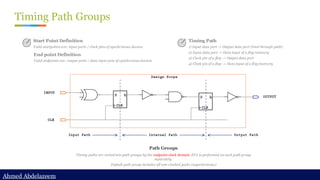
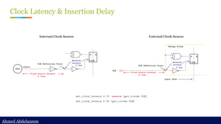
Static timing analysis (STA) is a method of validating the timing performance of a design by checking all possible paths for timing violations. STA breaks a design down into timing paths, calculates the signal propagation delay along each path, and checks for violations of timing constraints inside the design and at the input/output interface.

![Ahmed Abdelazeem
Ahmed Abdelazeem
Topic 16: report clock path
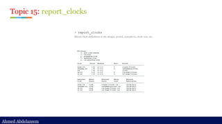
> report_timing -from [all_fanout -flat -clock_tree -levels 0] -to id_stage_0/clock -nosp
Report_timing to the clock pin of the sequential to check its clock path.
Note: the timing report would show the path is unconstrained
> Functional clock path
Timing path is going through
C3176/A1](https://image.slidesharecdn.com/constraintdevelop-250606153235-d8296a49/85/Back2School-Constraint-Develop-pdf-Chapter-3-36-320.jpg)
![Ahmed Abdelazeem
Ahmed Abdelazeem
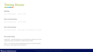
Topic 17: Show unconstrained path
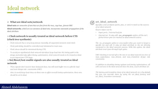
> Switch to show unconstrained path if there is any
set_app_var timing_report_uncontrained_path [true|false]
By default, report_timing or get_timing_paths command will only search for constrained path.
But sometimes we want to debug unconstrained path, so by turning it on, it allows you to check
timing path in most cases even if it is not constrained.](https://image.slidesharecdn.com/constraintdevelop-250606153235-d8296a49/85/Back2School-Constraint-Develop-pdf-Chapter-3-37-320.jpg)
![Ahmed Abdelazeem
Ahmed Abdelazeem
Ideal network
Step 1: set_ideal_network at the clock source
set_ideal_network [get_ports clock]
Original clock path](https://image.slidesharecdn.com/constraintdevelop-250606153235-d8296a49/85/Back2School-Constraint-Develop-pdf-Chapter-3-39-320.jpg)
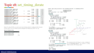
![Ahmed Abdelazeem
Ahmed Abdelazeem
Ideal network
Rule #1:
A combinational cell is marked as ideal if all of its input pins are either ideal or
attached to a constant net (and other input pins are ideal).
Setting the tenable to be ideal so u3479 will also become ideal
Step 2: set_ideal_network at the tenable port
set_ideal_network [get_ports tenable]](https://image.slidesharecdn.com/constraintdevelop-250606153235-d8296a49/85/Back2School-Constraint-Develop-pdf-Chapter-3-40-320.jpg)
![Ahmed Abdelazeem
Ahmed Abdelazeem
Ideal network
Step 1: set_ideal_network with no_propagate
set_ideal_network [get_nets cachememory/n3490] -no_propagate
Original clock path Rule #2
The size_only attribute is set on all cells of ideal network sources. If nets are specified, size_only
is set on all cells that are cells of the specified nets' global driver pins. This guarantees that ideal
network sources are not optimized away by compile.](https://image.slidesharecdn.com/constraintdevelop-250606153235-d8296a49/85/Back2School-Constraint-Develop-pdf-Chapter-3-41-320.jpg)
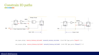
![Ahmed Abdelazeem
Ahmed Abdelazeem
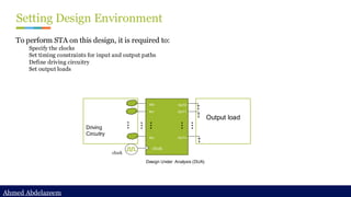
Constrain IO paths (cont’d)
set_driving_cell
set_driving_cell -lib_cell BFN [get_ports A]
set_load
set_load [get_attribute [get_lib_pins NAND2/A1] pin_capacitance]
[get_ports B]](https://image.slidesharecdn.com/constraintdevelop-250606153235-d8296a49/85/Back2School-Constraint-Develop-pdf-Chapter-3-44-320.jpg)


![[Back2School] Delay Calculation- Chapter 2](https://cdn.slidesharecdn.com/ss_thumbnails/delaycalculation-250530192911-03116e20-thumbnail.jpg?width=640&height=640&fit=bounds)


![[Back2School] Timing Checks- Chapter 5.pdf](https://cdn.slidesharecdn.com/ss_thumbnails/specialtimingchecks-250609185635-cf7ed43c-thumbnail.jpg?width=640&height=640&fit=bounds)
![[Back2School] STA Methodology- Chapter 7pdf](https://cdn.slidesharecdn.com/ss_thumbnails/stamethodology-250624214856-5fd24ebc-thumbnail.jpg?width=640&height=640&fit=bounds)
![[Back2School] STA Basic Concepts- Chapter 1.pdf](https://cdn.slidesharecdn.com/ss_thumbnails/stabasicconcepts-250524204554-25ac4895-thumbnail.jpg?width=640&height=640&fit=bounds)
![[Back2School] Crosstalk and Noise- Chapter 6.pdf](https://cdn.slidesharecdn.com/ss_thumbnails/crosstalkandnoise-250624214313-69c347be-thumbnail.jpg?width=640&height=640&fit=bounds)


![[Back2School] Timing Verification- Chapter 4](https://cdn.slidesharecdn.com/ss_thumbnails/timingverification-250607212312-4e8e2612-thumbnail.jpg?width=640&height=640&fit=bounds)


