B. Shiva Kumar et al Int. Journal of Engineering Research and Applications www.ijera.com
ISSN : 2248-9622, Vol. 4, Issue 5( Version 4), May 2014, pp.85-90
www.ijera.com 85 | P a g e
Analysis of New Dynamic Comparator for ADC Circuit
B. Shiva Kumar *, Fazal Noorbasha**, K. Vinay Kumar ***, N. V. Siva Rama
Krishna. T****
* (Student of VLSI Systems Research Group, Department of Electronics and Communication Engineering, K.L
University, Guntur-522502, AP-INDIA)
** (ASSOC. Professor VLSI Systems Research Group, Department of Electronics and Communication
Engineering, K.L University, Guntur-522502, AP-INDIA)
*** (Student of VLSI Systems Research Group, Department of Electronics and Communication Engineering,
K.L University, Guntur-522502, AP-INDIA)
**** (Student of VLSI Systems Research Group, Department of Electronics and Communication Engineering,
K.L University, Guntur-522502, AP-INDIA)
ABSTRACT
Comparator is the main basic device mostly used in analog to digital converters (ADC). For the better
transmission of signals, requirement of fastest analog to digital converters are required. So the new dynamic
comparator is replaced in the place of existing comparator of analog to digital converter for the better
conversion. This is designed and the performance is evaluated using CADENCE GPDK 180nm technology in
LINUX environment. The clock frequency of new ADC circuit is increased from 200MHZ to 250MHZ and
voltage is reduced from 1.2v to 0.2v. The power dissipation is decreased from 1.63619mw to 321.032µw for 1-
bit ADC and 1.2765mw to 82.346µw for 2-bit ADC.
Keyword- Analog to digital converter, Dynamic Comparator
I. INTRODUCTION
Analog to digital converter (ADC) mainly
converts an input analog value to digital
representation. The conversion is mainly done by
converting binary value to an output voltage.
Comparator is the main basic device used in the
Analog to digital converter (ADC) to compare the
two signals or two voltage values. Now a day’s need
for Analog to digital conversion (ADC) is increasing
for better transmission of signals. So the high speed
and low voltage Analog to digital converters (ADC)
is required.
Analog to digital converters (ADC) are of
mainly divided into four groups. They are Parallel
design, Digital to analog converter based design,
Integrator based design, Sigma delta design ADC.
When compared with other type of ADC’s Flash
ADC is faster. The new proposed comparator is
designed and replaced with existing comparator of
ADC for better ADC circuit. In Analog to digital
converters it is required to sample the input, so the
comparator is mainly used.
Dynamic comparators are mainly used in
ADC’s because these comparators are high speed,
consume less power dissipation, having zero static
power consumption and provide full swing digital
level output voltage in shorter duration. So 1-bit and
2-bit Flash ADC is used and proposed comparator is
placed in it. Delay of signals should be reduced in
ADC processing for faster conversion. ADC’s plays a
main role in mobile communication to convert the
voice for transmission. So ADC’s requirement is
more for easy conversion. As the comparator is main
basic device for ADC, the requirement of better
comparator is increasing.
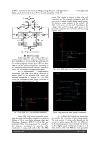
Proposed comparator [1]
is mainly designed
based upon the double tail structure as it consumes
low voltage and it has better performance. In this
external transistors are added to the double tail
dynamic comparator for the positive feedback
generation. The latch generation speed is increased in
proposed comparator. Two transistors M3 and M4
are designed in cross coupled manner for positive
feedback generation. The external transistors added
in the proposed comparator plays crucial role in the
operation of the comparator. The proposed double
tail comparator is shown in the below figure.1.
In this paper analysis is done on the ADC
circuit with the New Dynamic Comparator in the
place of Normal comparator. As the new dynamic
comparator has less delay and better performance.
The power dissipation, delay, voltage levels are
calculated in the analysis of the ADC circuit. By this
analysis the new ADC circuit can be designed. By
this new ADC circuit the better conversion can be
done with less power dissipation. In future this new
ADC can be replaced with the existing ADC circuit
for conversion of analog signal.
RESEARCH ARTICLE OPEN ACCESS
B. Shiva Kumar et al Int. Journal of Engineering Research and Applications www.ijera.com
ISSN : 2248-9622, Vol. 4, Issue 5( Version 4), May 2014, pp.85-90
www.ijera.com 86 | P a g e
Fig.1.Proposed Comparator
II. PROPOSED ADC
In this paper 1-bit and 2-bit Flash ADC’s are
mainly designed with new proposed comparator and
their performances are evaluated. The performances
are mainly compared with the 1-bit and 2-bit flash
ADC’s with the normal comparators. Depending on
the number of input bits to be converted the resistor
values and total number of comparators depends.
For ‘N’ number of bits, 2N-1
comparators are
required for Flash ADC circuit for the conversion of
analog signal. In the proposed ADC mainly the
proposed comparator is replaced. In 1-bit ADC
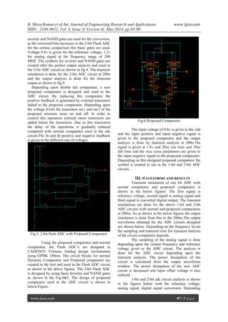
circuit one comparator is used for the conversion of
one bit analog signal as shown in Fig.2.
Fig.2. 1-bit flash ADC with Normal Comparator
In the 1-bit ADC circuit depending on the
input levels the total numbers of resistors are selected.
Voltage of 0.8v is given for the reference voltage and
1.2voltage, frequency 100M*(17/1024) HZ and
amplitude 550mv for analog signal. The symbol for
the proposed comparator is generated after
verification of output and used in the 1-bit ADC
circuit. The voltage is reduced to half value and
transmitted to the proposed comparator and the
conversion of analog signal to digital signal is done.
The transient output analysis of the normal 1-bit
ADC circuit is shown in the fig.7. Depending on the
voltage value and the analog signal given to the
proposed comparator the conversion of the analog
signal is done.
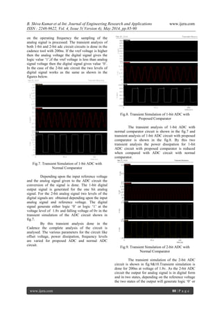
Fig.3. 1-bit flash ADC with Proposed Comparator
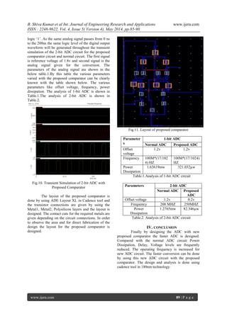
Fig.4. 2-bit flash ADC with Normal Comparator
In 2-bit Flash ADC mainly four comparators
are used for the conversion of two analog signals.
The total number of resistors also depends on the
number of analog signals. In the 2-bit ADC, two
levels of analog signals are transmitted and the two
levels of digital signals are obtained at output level of
ADC. In this 2-bit Flash ADC the basic gates like
B. Shiva Kumar et al Int. Journal of Engineering Research and Applications www.ijera.com
ISSN : 2248-9622, Vol. 4, Issue 5( Version 4), May 2014, pp.85-90
www.ijera.com 87 | P a g e
inverter and NAND gates are used for the conversion,
as the converted bits increases in the 2-bit Flash ADC
for the certain comparison this basic gates are used.
Voltage 0.8v is given for the reference voltage, 1.2v
for analog signal at the frequency range of 200
MHZ .The symbols for inverter and NAND gates are
created after the perfect output analysis and used in
the 2-bit ADC circuit as shown in fig.4. The transient
simulation is done for the 2-bit ADC circuit at 200n
and the output analysis is done for the transient
output as shown in fig.9.
Depending upon double tail comparator, a new
proposed comparator is designed and used in the
ADC circuit. By replacing this comparator the
positive feedback is generated by external transistors
added to the proposed comparator. Depending upon
the voltage levels the transistors mc1 and mc2 of the
proposed structure turns on and off. In order to
control this operation external nmos transistors are
added below the transistors. Due to this transistors
the delay of the operations is gradually reduced
compared with normal comparator used in the adc
circuit.The fn and fp positive and negative feedback
is given in the different rate of voltages.
Fig.5. 2-bit flash ADC with Proposed Comparator
Using the proposed comparator and normal
comparator, the Flash ADC’s are designed in
CADENCE Virtuoso Analog design environment
using GPDK 180nm. The circuit blocks for normal
Dynamic Comparator and Proposed comparator are
created in the tool and used in the Flash ADC circuit
as shown in the above figures. The 2-bit Flash ADC
is designed by using basic Inverter and NAND gates
as shown in the Fig.4&5. The design of proposed
comparator used in the ADC circuit is shown in
below Figure.
Fig.6.Proposed Comparator
The input voltage of 0.8v is given to the vdd
and the input positive and input negative signal is
given to the proposed comparator and the output
analysis is done by transient analysis at 200n.The
signal is given at 1.8v and 20ns rise time and 10ns
fall time and the vice versa parameters are given to
the input negative signal to the proposed comparator.
Depending on this designed proposed comparator the
symbol is created to use in the 1-bit and 2-bit ADC
circuits.
III. WAVEFORMS AND RESULTS
Transient simulation of one bit ADC with
normal comparator and proposed comparator is
shown in the below figures. The first signal is
reference voltage, second signal is analog signal and
third signal is converted digital output. The transient
simulations are done for the above 1-bit and 2-bit
ADC circuits with normal and proposed comparators
at 200ns. So as shown in the below figures the output
simulation is done from 0ns to the 200ns.The output
waveforms obtained for the ADC circuits designed
are shown below. Depending on the frequency levels
the sampling and transient time for transient analysis
of the circuit completely depends.
The sampling of the analog signal is done
depending upon the certain frequency and reference
voltage given to the ADC circuit. The analysis is
done for the ADC circuit depending upon the
transient analysis. The power dissipation of the
circuit is calculated from the output waveforms
window. The power dissipation of the new ADC
circuit is decreased and input offset voltage is also
reduced.
1-bit and 2-bit adc circuit analysis is shown
in the figures below with the reference voltage,
analog signal, digital signal conversion. Depending
B. Shiva Kumar et al Int. Journal of Engineering Research and Applications www.ijera.com
ISSN : 2248-9622, Vol. 4, Issue 5( Version 4), May 2014, pp.85-90
www.ijera.com 88 | P a g e
on the operating frequency the sampling of the
analog signal is processed. The transient analysis of
both 1-bit and 2-bit adc circuit circuits is done in the
cadence tool with 200ns. If the vref voltage is higher
then the analog voltage the digital signal gives the
logic value ‘1’,if the vref voltage is less than analog
signal voltage then the digital signal gives value ‘0’.
In the case of the 2-bit adc circuit the two levels of
digital signal works as the same as shown in the
figures below.
Fig.7. Transient Simulation of 1-bit ADC with
Normal Comparator
Depending upon the input reference voltage
and the analog signal given to the ADC circuit the
conversion of the signal is done. The 1-bit digital
output signal is generated for the one bit analog
signal. For the 2-bit analog signal two levels of the
digital signals are obtained depending upon the input
analog signal and reference voltage. The digital
signal generate either logic ‘0’ or logic ‘1’ at the
voltage level of 1.8v and falling voltage of 0v in the
transient simulation of the ADC circuit shown in
fig.7.
By this transient analysis done in the
Cadence the complete analysis of the circuit is
analysed. The various parameters for the circuit like
offset voltage, power dissipation, frequency levels
are varied for proposed ADC and normal ADC
circuit.
Fig.8. Transient Simulation of 1-bit ADC with
Proposed Comparator
The transient analysis of 1-bit ADC with
normal comparator circuit is shown in the fig.7 and
transient analysis of 1-bit ADC circuit with proposed
comparator is shown in the fig.8. By this two
transient analysis the power dissipation for 1-bit
ADC circuit with proposed comparator is reduced
when compared with ADC circuit with normal
comparator.
Fig.9. Transient Simulation of 2-bit ADC with
Normal Comparator
The transient simulation of the 2-bit ADC
circuit is shown in fig.9&10.Transient simulation is
done for 200ns at voltage of 1.8v. As the 2-bit ADC
circuit the output for analog signal is in digital form
and in two states, depending on the reference voltage
the two states of the output will generate logic ‘0’ or
B. Shiva Kumar et al Int. Journal of Engineering Research and Applications www.ijera.com
ISSN : 2248-9622, Vol. 4, Issue 5( Version 4), May 2014, pp.85-90
www.ijera.com 89 | P a g e
logic ‘1’. As the same analog signal passes from 0 ns
to the 200ns the same logic level of the digital output
waveform will be generated throughout the transient
simulation of the 2-bit ADC circuit for the proposed
comparator circuit and normal circuit. The first signal
is reference voltage of 1.8v and second signal is the
analog signal given for the conversion. The
parameters of the analog signal are shown in the
below table.1.By this table the various parameters
varied with the proposed comparator can be clearly
known with the table shown below. The various
parameters like offset voltage, frequency, power
dissipation. The analysis of 1-bit ADC is shown in
Table.1.The analysis of 2-bit ADC is shown in
Table.2.
Fig.10. Transient Simulation of 2-bit ADC with
Proposed Comparator
The layout of the proposed comparator is
done by using ADE Layout XL in Cadence tool and
the transistor connections are given by using the
Metal1, Metal2, Polysilicon layers and the layout is
designed. The contact cuts for the required metals are
given depending on the circuit connections. In order
to observe the area and for direct fabrication of the
design the layout for the proposed comparator is
designed.
Fig.11. Layout of proposed comparator
Table.1.Analysis of 1-bit ADC circuit
Table.2. Analysis of 2-bit ADC circuit
IV. CONCLUSION
Finally by designing the ADC with new
proposed comparator the faster ADC is designed.
Compared with the normal ADC circuit Power
Dissipation, Delay, Voltage levels are frequently
reduced. The operating frequency is increased for
new ADC circuit. The faster conversion can be done
by using this new ADC circuit with the proposed
comparator. The design and analysis is done using
cadence tool in 180nm technology.
Parameter
s
1-bit ADC
Normal ADC Proposed ADC
Offset
voltage
1.2v 1.2v
Frequency 100M*(17/102
4) HZ
100M*(17/1024)
HZ
Power
Dissipation
1.63619mw 321.032µw
Parameters 2-bit ADC
Normal ADC Proposed
ADC
Offset voltage 1.2v 0.2v
Frequency 200 MHZ 250MHZ
Power
Dissipation
1.2765mw 82.346µw
B. Shiva Kumar et al Int. Journal of Engineering Research and Applications www.ijera.com
ISSN : 2248-9622, Vol. 4, Issue 5( Version 4), May 2014, pp.85-90
www.ijera.com 90 | P a g e
REFERENCES
[1]. Samaneh Babayan Mashhadi and Reza
Lotfi ”Analysis and Design of a Low
Voltage Low Power Double Tail
Comparator”, IEEE Trans on VLSI systems,
vol.22, no.2, pp.343-352, Feb 2014.
[2]. S.U.Ay.”A sub 1-volt 10 bit supply boosted
SAR ADC design in standard CMOS”,
Analog integrated circuits, vol.66, no.2,
pp.213-221, Feb 2011.
[3]. S.Babayan-Mashhadi and R. Lotfi, ”an
offset cancellation technique for
comparators using body-voltage trimming”
J.analog integr circuits signal process vol.73,
no.3, pp.673- 682, dec 2012
[4] A. Mesgarani, M. N. Alam, F. Z. Nelson and
S. U. Ay,” Supply boosting technique for
designing very low voltage mixed signals
circuits in standard CMOS”, pp.893-
896,IEEE,Aug 2010.
[5]. B. Goll and H. Zimmermann, ”A
comparator with reduced delay time in 65
nm CMOS for supply voltages down to
0.65”, IEEE Trans, vol.56, no.11, pp.810-
814, Nov 2009.

N045048590

  • 1.
    B. Shiva Kumaret al Int. Journal of Engineering Research and Applications www.ijera.com ISSN : 2248-9622, Vol. 4, Issue 5( Version 4), May 2014, pp.85-90 www.ijera.com 85 | P a g e Analysis of New Dynamic Comparator for ADC Circuit B. Shiva Kumar *, Fazal Noorbasha**, K. Vinay Kumar ***, N. V. Siva Rama Krishna. T**** * (Student of VLSI Systems Research Group, Department of Electronics and Communication Engineering, K.L University, Guntur-522502, AP-INDIA) ** (ASSOC. Professor VLSI Systems Research Group, Department of Electronics and Communication Engineering, K.L University, Guntur-522502, AP-INDIA) *** (Student of VLSI Systems Research Group, Department of Electronics and Communication Engineering, K.L University, Guntur-522502, AP-INDIA) **** (Student of VLSI Systems Research Group, Department of Electronics and Communication Engineering, K.L University, Guntur-522502, AP-INDIA) ABSTRACT Comparator is the main basic device mostly used in analog to digital converters (ADC). For the better transmission of signals, requirement of fastest analog to digital converters are required. So the new dynamic comparator is replaced in the place of existing comparator of analog to digital converter for the better conversion. This is designed and the performance is evaluated using CADENCE GPDK 180nm technology in LINUX environment. The clock frequency of new ADC circuit is increased from 200MHZ to 250MHZ and voltage is reduced from 1.2v to 0.2v. The power dissipation is decreased from 1.63619mw to 321.032µw for 1- bit ADC and 1.2765mw to 82.346µw for 2-bit ADC. Keyword- Analog to digital converter, Dynamic Comparator I. INTRODUCTION Analog to digital converter (ADC) mainly converts an input analog value to digital representation. The conversion is mainly done by converting binary value to an output voltage. Comparator is the main basic device used in the Analog to digital converter (ADC) to compare the two signals or two voltage values. Now a day’s need for Analog to digital conversion (ADC) is increasing for better transmission of signals. So the high speed and low voltage Analog to digital converters (ADC) is required. Analog to digital converters (ADC) are of mainly divided into four groups. They are Parallel design, Digital to analog converter based design, Integrator based design, Sigma delta design ADC. When compared with other type of ADC’s Flash ADC is faster. The new proposed comparator is designed and replaced with existing comparator of ADC for better ADC circuit. In Analog to digital converters it is required to sample the input, so the comparator is mainly used. Dynamic comparators are mainly used in ADC’s because these comparators are high speed, consume less power dissipation, having zero static power consumption and provide full swing digital level output voltage in shorter duration. So 1-bit and 2-bit Flash ADC is used and proposed comparator is placed in it. Delay of signals should be reduced in ADC processing for faster conversion. ADC’s plays a main role in mobile communication to convert the voice for transmission. So ADC’s requirement is more for easy conversion. As the comparator is main basic device for ADC, the requirement of better comparator is increasing. Proposed comparator [1] is mainly designed based upon the double tail structure as it consumes low voltage and it has better performance. In this external transistors are added to the double tail dynamic comparator for the positive feedback generation. The latch generation speed is increased in proposed comparator. Two transistors M3 and M4 are designed in cross coupled manner for positive feedback generation. The external transistors added in the proposed comparator plays crucial role in the operation of the comparator. The proposed double tail comparator is shown in the below figure.1. In this paper analysis is done on the ADC circuit with the New Dynamic Comparator in the place of Normal comparator. As the new dynamic comparator has less delay and better performance. The power dissipation, delay, voltage levels are calculated in the analysis of the ADC circuit. By this analysis the new ADC circuit can be designed. By this new ADC circuit the better conversion can be done with less power dissipation. In future this new ADC can be replaced with the existing ADC circuit for conversion of analog signal. RESEARCH ARTICLE OPEN ACCESS
  • 2.
    B. Shiva Kumaret al Int. Journal of Engineering Research and Applications www.ijera.com ISSN : 2248-9622, Vol. 4, Issue 5( Version 4), May 2014, pp.85-90 www.ijera.com 86 | P a g e Fig.1.Proposed Comparator II. PROPOSED ADC In this paper 1-bit and 2-bit Flash ADC’s are mainly designed with new proposed comparator and their performances are evaluated. The performances are mainly compared with the 1-bit and 2-bit flash ADC’s with the normal comparators. Depending on the number of input bits to be converted the resistor values and total number of comparators depends. For ‘N’ number of bits, 2N-1 comparators are required for Flash ADC circuit for the conversion of analog signal. In the proposed ADC mainly the proposed comparator is replaced. In 1-bit ADC circuit one comparator is used for the conversion of one bit analog signal as shown in Fig.2. Fig.2. 1-bit flash ADC with Normal Comparator In the 1-bit ADC circuit depending on the input levels the total numbers of resistors are selected. Voltage of 0.8v is given for the reference voltage and 1.2voltage, frequency 100M*(17/1024) HZ and amplitude 550mv for analog signal. The symbol for the proposed comparator is generated after verification of output and used in the 1-bit ADC circuit. The voltage is reduced to half value and transmitted to the proposed comparator and the conversion of analog signal to digital signal is done. The transient output analysis of the normal 1-bit ADC circuit is shown in the fig.7. Depending on the voltage value and the analog signal given to the proposed comparator the conversion of the analog signal is done. Fig.3. 1-bit flash ADC with Proposed Comparator Fig.4. 2-bit flash ADC with Normal Comparator In 2-bit Flash ADC mainly four comparators are used for the conversion of two analog signals. The total number of resistors also depends on the number of analog signals. In the 2-bit ADC, two levels of analog signals are transmitted and the two levels of digital signals are obtained at output level of ADC. In this 2-bit Flash ADC the basic gates like
  • 3.
    B. Shiva Kumaret al Int. Journal of Engineering Research and Applications www.ijera.com ISSN : 2248-9622, Vol. 4, Issue 5( Version 4), May 2014, pp.85-90 www.ijera.com 87 | P a g e inverter and NAND gates are used for the conversion, as the converted bits increases in the 2-bit Flash ADC for the certain comparison this basic gates are used. Voltage 0.8v is given for the reference voltage, 1.2v for analog signal at the frequency range of 200 MHZ .The symbols for inverter and NAND gates are created after the perfect output analysis and used in the 2-bit ADC circuit as shown in fig.4. The transient simulation is done for the 2-bit ADC circuit at 200n and the output analysis is done for the transient output as shown in fig.9. Depending upon double tail comparator, a new proposed comparator is designed and used in the ADC circuit. By replacing this comparator the positive feedback is generated by external transistors added to the proposed comparator. Depending upon the voltage levels the transistors mc1 and mc2 of the proposed structure turns on and off. In order to control this operation external nmos transistors are added below the transistors. Due to this transistors the delay of the operations is gradually reduced compared with normal comparator used in the adc circuit.The fn and fp positive and negative feedback is given in the different rate of voltages. Fig.5. 2-bit flash ADC with Proposed Comparator Using the proposed comparator and normal comparator, the Flash ADC’s are designed in CADENCE Virtuoso Analog design environment using GPDK 180nm. The circuit blocks for normal Dynamic Comparator and Proposed comparator are created in the tool and used in the Flash ADC circuit as shown in the above figures. The 2-bit Flash ADC is designed by using basic Inverter and NAND gates as shown in the Fig.4&5. The design of proposed comparator used in the ADC circuit is shown in below Figure. Fig.6.Proposed Comparator The input voltage of 0.8v is given to the vdd and the input positive and input negative signal is given to the proposed comparator and the output analysis is done by transient analysis at 200n.The signal is given at 1.8v and 20ns rise time and 10ns fall time and the vice versa parameters are given to the input negative signal to the proposed comparator. Depending on this designed proposed comparator the symbol is created to use in the 1-bit and 2-bit ADC circuits. III. WAVEFORMS AND RESULTS Transient simulation of one bit ADC with normal comparator and proposed comparator is shown in the below figures. The first signal is reference voltage, second signal is analog signal and third signal is converted digital output. The transient simulations are done for the above 1-bit and 2-bit ADC circuits with normal and proposed comparators at 200ns. So as shown in the below figures the output simulation is done from 0ns to the 200ns.The output waveforms obtained for the ADC circuits designed are shown below. Depending on the frequency levels the sampling and transient time for transient analysis of the circuit completely depends. The sampling of the analog signal is done depending upon the certain frequency and reference voltage given to the ADC circuit. The analysis is done for the ADC circuit depending upon the transient analysis. The power dissipation of the circuit is calculated from the output waveforms window. The power dissipation of the new ADC circuit is decreased and input offset voltage is also reduced. 1-bit and 2-bit adc circuit analysis is shown in the figures below with the reference voltage, analog signal, digital signal conversion. Depending
  • 4.
    B. Shiva Kumaret al Int. Journal of Engineering Research and Applications www.ijera.com ISSN : 2248-9622, Vol. 4, Issue 5( Version 4), May 2014, pp.85-90 www.ijera.com 88 | P a g e on the operating frequency the sampling of the analog signal is processed. The transient analysis of both 1-bit and 2-bit adc circuit circuits is done in the cadence tool with 200ns. If the vref voltage is higher then the analog voltage the digital signal gives the logic value ‘1’,if the vref voltage is less than analog signal voltage then the digital signal gives value ‘0’. In the case of the 2-bit adc circuit the two levels of digital signal works as the same as shown in the figures below. Fig.7. Transient Simulation of 1-bit ADC with Normal Comparator Depending upon the input reference voltage and the analog signal given to the ADC circuit the conversion of the signal is done. The 1-bit digital output signal is generated for the one bit analog signal. For the 2-bit analog signal two levels of the digital signals are obtained depending upon the input analog signal and reference voltage. The digital signal generate either logic ‘0’ or logic ‘1’ at the voltage level of 1.8v and falling voltage of 0v in the transient simulation of the ADC circuit shown in fig.7. By this transient analysis done in the Cadence the complete analysis of the circuit is analysed. The various parameters for the circuit like offset voltage, power dissipation, frequency levels are varied for proposed ADC and normal ADC circuit. Fig.8. Transient Simulation of 1-bit ADC with Proposed Comparator The transient analysis of 1-bit ADC with normal comparator circuit is shown in the fig.7 and transient analysis of 1-bit ADC circuit with proposed comparator is shown in the fig.8. By this two transient analysis the power dissipation for 1-bit ADC circuit with proposed comparator is reduced when compared with ADC circuit with normal comparator. Fig.9. Transient Simulation of 2-bit ADC with Normal Comparator The transient simulation of the 2-bit ADC circuit is shown in fig.9&10.Transient simulation is done for 200ns at voltage of 1.8v. As the 2-bit ADC circuit the output for analog signal is in digital form and in two states, depending on the reference voltage the two states of the output will generate logic ‘0’ or
  • 5.
    B. Shiva Kumaret al Int. Journal of Engineering Research and Applications www.ijera.com ISSN : 2248-9622, Vol. 4, Issue 5( Version 4), May 2014, pp.85-90 www.ijera.com 89 | P a g e logic ‘1’. As the same analog signal passes from 0 ns to the 200ns the same logic level of the digital output waveform will be generated throughout the transient simulation of the 2-bit ADC circuit for the proposed comparator circuit and normal circuit. The first signal is reference voltage of 1.8v and second signal is the analog signal given for the conversion. The parameters of the analog signal are shown in the below table.1.By this table the various parameters varied with the proposed comparator can be clearly known with the table shown below. The various parameters like offset voltage, frequency, power dissipation. The analysis of 1-bit ADC is shown in Table.1.The analysis of 2-bit ADC is shown in Table.2. Fig.10. Transient Simulation of 2-bit ADC with Proposed Comparator The layout of the proposed comparator is done by using ADE Layout XL in Cadence tool and the transistor connections are given by using the Metal1, Metal2, Polysilicon layers and the layout is designed. The contact cuts for the required metals are given depending on the circuit connections. In order to observe the area and for direct fabrication of the design the layout for the proposed comparator is designed. Fig.11. Layout of proposed comparator Table.1.Analysis of 1-bit ADC circuit Table.2. Analysis of 2-bit ADC circuit IV. CONCLUSION Finally by designing the ADC with new proposed comparator the faster ADC is designed. Compared with the normal ADC circuit Power Dissipation, Delay, Voltage levels are frequently reduced. The operating frequency is increased for new ADC circuit. The faster conversion can be done by using this new ADC circuit with the proposed comparator. The design and analysis is done using cadence tool in 180nm technology. Parameter s 1-bit ADC Normal ADC Proposed ADC Offset voltage 1.2v 1.2v Frequency 100M*(17/102 4) HZ 100M*(17/1024) HZ Power Dissipation 1.63619mw 321.032µw Parameters 2-bit ADC Normal ADC Proposed ADC Offset voltage 1.2v 0.2v Frequency 200 MHZ 250MHZ Power Dissipation 1.2765mw 82.346µw
  • 6.
    B. Shiva Kumaret al Int. Journal of Engineering Research and Applications www.ijera.com ISSN : 2248-9622, Vol. 4, Issue 5( Version 4), May 2014, pp.85-90 www.ijera.com 90 | P a g e REFERENCES [1]. Samaneh Babayan Mashhadi and Reza Lotfi ”Analysis and Design of a Low Voltage Low Power Double Tail Comparator”, IEEE Trans on VLSI systems, vol.22, no.2, pp.343-352, Feb 2014. [2]. S.U.Ay.”A sub 1-volt 10 bit supply boosted SAR ADC design in standard CMOS”, Analog integrated circuits, vol.66, no.2, pp.213-221, Feb 2011. [3]. S.Babayan-Mashhadi and R. Lotfi, ”an offset cancellation technique for comparators using body-voltage trimming” J.analog integr circuits signal process vol.73, no.3, pp.673- 682, dec 2012 [4] A. Mesgarani, M. N. Alam, F. Z. Nelson and S. U. Ay,” Supply boosting technique for designing very low voltage mixed signals circuits in standard CMOS”, pp.893- 896,IEEE,Aug 2010. [5]. B. Goll and H. Zimmermann, ”A comparator with reduced delay time in 65 nm CMOS for supply voltages down to 0.65”, IEEE Trans, vol.56, no.11, pp.810- 814, Nov 2009.