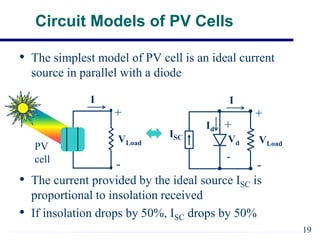
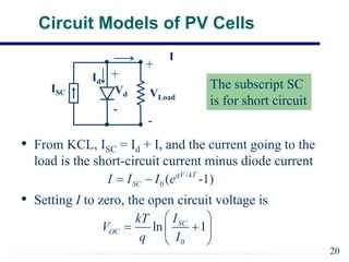
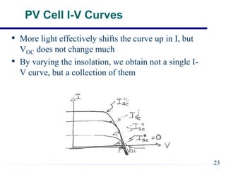
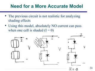
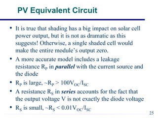
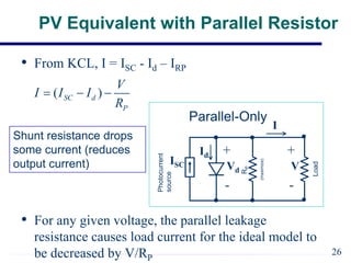
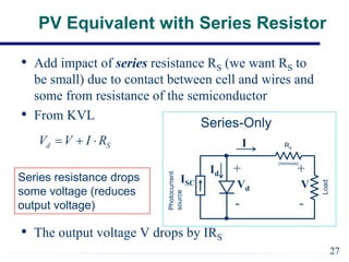
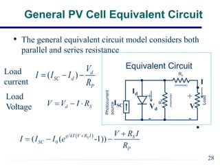
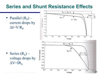
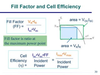
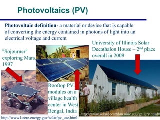
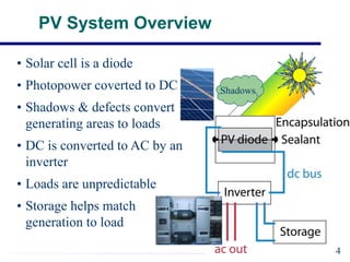
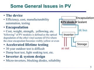
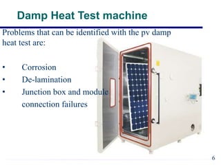
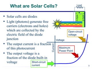
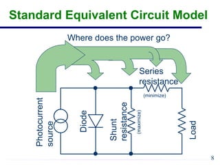
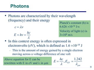
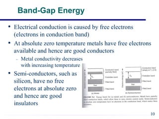
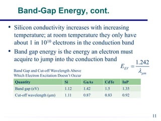
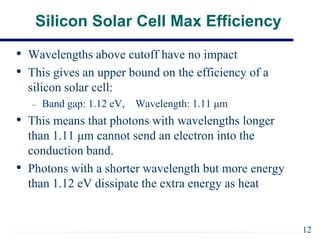
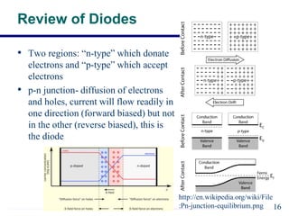
EE421 Renewable Energy Systems covers solar PV systems. Photovoltaics (PV) directly convert sunlight into electricity using solar cells. Rooftop PV modules are used to power village health centers in India. PV technology has improved over time, with costs recently dropping substantially. A PV system uses solar modules to generate DC power, then an inverter converts it to AC power for loads. Shadows and defects can reduce generating areas to loads in the system. General issues in PV include device efficiency and cost, encapsulation durability, and testing to verify 30-year lifespan. Solar cells function like diodes, using the photovoltaic effect to generate current from sunlight. Proper modeling of solar cells includes accounting for
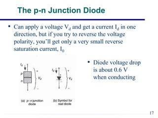
![The p-n Junction Diode
Voltage-Current (VI) characteristics for a diode
/
0 ( -1)
d
qV kT
d
I I e
38.9
0 ( -1) (at 25 C)
d
V
d
I I e
k = Boltzmann’s constant
1.381x10⁻²³ [J/K]
T = junction temperature [K]
Vd = diode voltage
Id = diode current
q = electron charge 1.602x10⁻¹⁹ C
I0 = reverse saturation current
18](https://image.slidesharecdn.com/reslecture11solarpv-220102063128/85/Res-lecture-11-solar-pv-18-320.jpg)