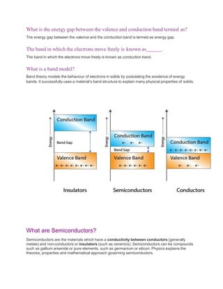
SlideShare a Scribd company logo
1 of 58
Important Questions For Viva
What is LED?
A light-emitting diode (LED) is a semiconductor device that emits light when an electric current
flows through it.
What is Light Emitting Diodes used for?
LEDs have a wide range of applications ranging from your mobile phone to large advertising
billboards. They mostly find applications in devices that show the time and display different
types of data.
How do LEDs work?
LEDs work on the principle of Electroluminescence. On passing a current through the diode,
minority charge carriers and majority charge carriers recombine at the junction. On
recombination, energy is released in the form of photons. As the forward voltage increases, the
intensity of the light increases and reaches a maximum.
What is Electroluminescence?
Electroluminescence is an optical phenomenon, and electrical phenomenon where a material
emits light in response to an electric current passed through it.
What are the advantages of LEDs?
LEDs consume less power, and they require low operational voltage. No warm-up time is needed
for LEDs.
Advantages of LEDs over Incandescent Power Lamps
Some advantages of LEDs over Incandescent Power Lamps are:
 LEDs consume less power, and they require low operational voltage.
 No warm-up time is needed for LEDs.
 The emitted light is monochromatic.
 They exhibit long life and ruggedness.
What determines the colour of an LED?
The colour of an LED is determined by the material used in the semiconducting element. The two
primary materials used in LEDs are aluminium gallium indium phosphide alloys and indium gallium
nitride alloys. Aluminium alloys are used to obtain red, orange and yellow light, and indium alloys are
used to get green, blue and white light. Slight changes in the composition of these alloys change the
colour of the emitted light.
Properties of Laser Light
Laser light is monochromatic, directional and coherent.
Laser Light is Monochromatic
Unlike white light, which is made of seven colours, laser light is made of a singlecolour.
Laser Light is Directional
Laser light is highly directional.
Laser Light is Coherent
Laser light is coherent because the wavelengths of the laser light are in phase in space and time.
Uses of LED
LEDs find applications in various fields, including optical communication, alarm and security
systems, remote-controlled operations, robotics, etc. It finds usage in many areas because of its
long-lasting capability, low power requirements, swift response time, and fast switching capabilities.
Below are a few standards LED uses:
 Used for TV back-lighting
 Used in displays
 Used in Automotives
 LEDs used in the dimming of lights
Types of LED
Below is the list of different types of LED that are designed using semiconductors:
 Miniature LEDs
 High-Power LEDs
 Flash LED
 Bi and Tri-Colour
 Red Green Blue LEDs
 Alphanumeric LED
 Lighting LED
How does an LED work?
When the diode is forward biased, the minority electrons are sent from p → n while the minority
holes are sent from n → p. At the junction boundary, the concentration of minority carriers increases.
The excess minority carriers at the junction recombine with the majority charges carriers.
The energy is released in the form of photons on recombination. In standard diodes, the energy is
released in the form of heat. But in light-emitting diodes, the energy is released in the form of
photons. We call this phenomenon electroluminescence. Electroluminescence is an optical
phenomenon, and electrical phenomenon where a material emits light in response to an electric
current passed through it. As the forward voltage increases, the intensity of the light increases and
reaches a maximum.
What Is Solar Energy?
Solar energy is defined as the transformation of energy that is present in the sun and is one of
the renewable energies. Once the sunlight passes through the earth’s atmosphere, most of it is in
the form of visible light and infrared radiation. Plants use it to convert into sugar and starches and
this process of conversion is known as photosynthesis. Solar cell panels are used to convert this
energy into electricity.
Solar Energy Advantages and Disadvantages
Advantages of solar energy are:
 Clean: It is considered to the cleanest form of energy as there is no emission of carbon
dioxide like in case of fossil fuels which is one of the causes of global warming.
 Renewable: There is an ample amount of energy available on earth as long as the sun
exists.
 Reliable: The energy can be stored in the batteries and so there is no question of
unreliability.
 Reduction in utility costs.
 Free energy because it can be trapped easily.
Disadvantages of solar energy:
 The production is low during winters and on cloudy days.
 Installation and the initial cost of the materials are expensive.
 Space consumption is more.
Types of Solar Energy
Solar energy can be classified into two categories depending upon the mode of conversion and type
of energy it is converted into. Passive solar energy and active solar energy belongs to the mode of
conversion and solar thermal energy, photovoltaic solar power and concentrating solar power.
 Passive solar energy: This refers to trapping sun’s energy without using any mechanical
devices.
 Active solar energy: This uses mechanical devices to collect, store and distribute the energy.
 Solar thermal energy: This is the energy obtained by converting solar energy into heat.
 Photovoltaic solar power: This is the energy obtained by converting solar energy into
electricity.
 Concentrating solar power: This is a type of solar thermal energy which is used to generate
solar power electricity.
Solar Energy Project
Solar energy – the experiment on the efficiency of the solar heating working model is one of the
easiest science experiment that you can prepare in your school fair science project. This working
model is quick, simple and very informative.
The result may vary if the project is performed outdoor due to the wind and weather condition, so it is
recommended to conduct the experiment indoors.
In this solar heater project, use reflectors to concentrating the solar energy in one small place to
collect and store heat energy. In this experiment, you will see the efficiency of solar energy.
Materials Required
1. A wooden stand
2. Thermometer
3. A concave or converging mirror
4. Tube to flow liquid.
5. Black paper
Procedure
1. Mount the wooden stand
2. Roll pieces of black paper around the tube.
3. Attach the tube in the concave mirror in a way where the sunlight concentrate in one
direction.
4. Fill the tube with tap water
5. After 30 minutes record the temperature of the tube.
Observations
To calculate the efficiency of the concave mirror solar heater, you can divide the temperature
increase by the direct sunlight. Eventually, the temperature of the water increase after 30 minutes as
the heat is transferred through the concave mirror and concentrated on the tube.
Uses Of Solar Energy
 Water heating: Solar energy is used to replace electric heaters and gas as efficiency is
more with 15-30%.
 Heating of swimming pools: Solar blankets are used to keep the pool warm. The other way
is by using a solar water heater to keep the water warm.
 Cooking purposes: Solar cookers are used for cooking food. Solar energy is used to heat,
cook and pasteurize the food. A solar cooker consists of an elevated heat sink such that
when food is placed in it, it gets cooked well.
Energy Bands Description
In gaseous substances, the arrangement of molecules are spread apart and are not so close to
each other. In liquids, the molecules are closer to each other. But, in solids, the molecules are
closely arranged together, due to this the atoms of molecules tend to move into the orbitals of
neighbouring atoms. Hence, the electron orbitals overlap when atoms come together.
In solids, several bands of energy levels are formed due to the intermixing of atoms in solids. We call
these set of energy levels as energy bands.
Formation of Energy Bands
In an isolated atom, the electrons in each orbit possess definite energy. But, in the case of solids,
the energy level of the outermost orbit electrons are affected by the neighbouring atoms.
When two isolated charges are brought close to each other, the electrons in the outermost orbit
experiences an attractive force from the nearest or neighbouring atomic nucleus. Due to this reason,
the energies of the electrons will not be at the same level, the energy levels of electrons are
changed to a value which is higher or lower than that of the original energy level of the electron.
The electrons in the same orbit exhibit different energy levels. The grouping of this different energy
levels is known as energy band.
However, the energy of the inner orbit electrons are not much affected by the presence of
neighbouring atoms.
Classification of Energy Bands
Valence Band
The electrons in the outermost shell are known as valence electrons. These valence electrons
contain a series of energy levels and form an energy band known as valence band. The valence
band has the highest occupied energy.
Conduction Band
The valence electrons are not tightly held to the nucleus due to which a few of these valence
electrons leave the outermost orbit even at room temperature and become free electrons. The free
electrons conduct current in conductors and are therefore known as conduction electrons. The
conduction band is one that contains conduction electrons and has the lowest occupied energy
levels.
Forbidden Energy Gap
The gap between the valence band and the conduction band is referred to as forbidden gap. As the
name suggests, the forbidden gap doesn’t have any energy and no electrons stay in this band. If the
forbidden energy gap is greater, then the valence band electrons are tightly bound or firmly attached
to the nucleus. We require some amount of external energy that is equal to the forbidden energy
gap.
The figure below shows the conduction band, valence band and the forbidden energy gap.
Conductors
Gold, Aluminium, Silver, Copper, all these metals allow an electric current to flow through them.
There is no forbidden gap between the valence band and conduction band which results in the
overlapping of both the bands. The number of free electrons available at room temperature is large.
Insulators
Glass and wood are examples of the insulator. These substances do not allow electricity to pass
through them. They have high resistivity and very low conductivity.
The energy gap in the insulator is very high up to 7eV. The material cannot conduct because the
movement of the electrons from the valence band to the conduction band is not possible.
Semiconductors
Germanium and Silicon are the most preferable material whose electrical properties lie in
between semiconductors and insulators. The energy band diagram of semiconductor is shown
where the conduction band is empty and the valence band is completely filled but the forbidden gap
between the two bands is very small that is about 1eV. For Germanium, the forbidden gap is 0.72eV
and for Silicon, it is 1.1eV. Thus, semiconductor requires small conductivity.
Energy Band Theory
According to Bohr’s theory, every shell of an atom contains a discrete amount of energy at different
levels. Energy band theory explains the interaction of electrons between the outermost shell and the
innermost shell. Based on the energy band theory, there are three different energy bands:
1. Valence band
2. Forbidden energy gap
3. Conduction band
Frequently Asked Questions – FAQs
The valence band and the conduction band overlap in .
The valence band and the conduction band overlap in conductors.
What is the energy that a valence electron should have to jump from valence
band to conduction band called?
The valence electrons must have the same energy as an energy gap to jump from valence band to
conduction band.
What is the energy gap between the valence and conduction band termed as?
The energy gap between the valence and the conduction band is termed as energy gap.
The band in which the electrons move freely is known as .
The band in which the electrons move freely is known as conduction band.
What is a band model?
Band theory models the behaviour of electrons in solids by postulating the existence of energy
bands. It successfully uses a material’s band structure to explain many physical properties of solids.
What are Semiconductors?
Semiconductors are the materials which have a conductivity between conductors (generally
metals) and non-conductors or insulators (such as ceramics). Semiconductors can be compounds
such as gallium arsenide or pure elements, such as germanium or silicon. Physics explains the
theories, properties and mathematical approach governing semiconductors.
Examples of Semiconductors:
Gallium arsenide, germanium, and silicon are some of the most commonly used semiconductors.
Silicon is used in electronic circuit fabrication and gallium arsenide is used in solar cells, laser
diodes, etc.
Holes and Electrons in Semiconductors
Holes and electrons are the types of charge carriers accountable for the flow of current in
semiconductors. Holes (valence electrons) are the positively charged electric charge carrier
whereas electrons are the negatively charged particles. Both electrons and holes are equal in
magnitude but opposite in polarity.
Mobility of Electrons and Holes
In a semiconductor, the mobility of electrons is higher than that of the holes. It is mainly
because of their different band structures and scattering mechanisms.
Electrons travel in the conduction band whereas holes travel in the valence band. When an electric
field is applied, holes cannot move as freely as electrons due to their restricted movent. The
elevation of electrons from their inner shells to higher shells results in the creation of holes in
semiconductors. Since the holes experience stronger atomic force by the nucleus than electrons,
holes have lower mobility.
The mobility of a particle in a semiconductor is more if;
 Effective mass of particles is lesser
 Time between scattering events is more
For intrinsic silicon at 300 K, the mobility of electrons is 1500 cm2 (V∙s)-1 and the mobility of holes is
475 cm2 (V∙s)-1.
The bond model of electrons in silicon of valency 4 is shown below. Here, when one of the free
electrons (blue dots) leaves the lattice position, it creates a hole (grey dots). This hole thus created
takes the opposite charge of the electron and can be imagined as positive charge carriers moving in
the lattice.
Band Theory of Semiconductors
The introduction of band theory happened during the quantum revolution in science. Walter Heitler
and Fritz London discovered the energy bands.
We know that the electrons in an atom are present in different energy levels. When we try to
assemble a lattice of a solid with N atoms, then each level of an atom must split up into N levels in
the solid. This splitting up of sharp and tightly packed energy levels forms Energy Bands. The gap
between adjacent bands representing a range of energies that possess no electron is called a Band
Gap.
Conduction Band and Valence Band in Semiconductors
Valence Band:
The energy band involving the energy levels of valence electrons is known as the valence band. It is
the highest occupied energy band. When compared with insulators, the bandgap in semiconductors
is smaller. It allows the electrons in the valence band to jump into the conduction band on receiving
any external energy.
Conduction Band:
It is the lowest unoccupied band that includes the energy levels of positive (holes) or negative (free
electrons) charge carriers. It has conducting electrons resulting in the flow of current. The conduction
band possess high energy level and are generally empty. The conduction band in semiconductors
accepts the electrons from the valence band.
What is Fermi Level in Semiconductors?
Fermi level (denoted by EF) is present between the valence and conduction bands. It is the highest
occupied molecular orbital at absolute zero. The charge carriers in this state have their own quantum
states and generally do not interact with each other. When the temperature rises above absolute
zero, these charge carriers will begin to occupy states above Fermi level.
In a p-type semiconductor, there is an increase in the density of unfilled states. Thus,
accommodating more electrons at the lower energy levels. However, in an n-type semiconductor,
the density of states increases, therefore, accommodating more electrons at higher energy levels.
Properties of Semiconductors
Semiconductors can conduct electricity under preferable conditions or circumstances. This unique
property makes it an excellent material to conduct electricity in a controlled manner as required.
Unlike conductors, the charge carriers in semiconductors arise only because of external energy
(thermal agitation). It causes a certain number of valence electrons to cross the energy gap and
jump into the conduction band, leaving an equal amount of unoccupied energy states, i.e. holes.
Conduction due to electrons and holes are equally important.
 Resistivity: 10-5 to 106 Ωm
 Conductivity: 105 to 10-6 mho/m
 Temperature coefficient of resistance: Negative
 Current Flow: Due to electrons and holes
Why does the Resistivity of Semiconductors go down with Temperature?
The difference in resistivity between conductors and semiconductors is due to their difference in
charge carrier density.
The resistivity of semiconductors decreases with temperature because the number of charge
carriers increases rapidly with increase in temperature, making the fractional change i.e. the
temperature coefficient negative.
Some Important Properties of Semiconductors are:
1. Semiconductor acts like an insulator at Zero Kelvin. On increasing the temperature, it works
as a conductor.
2. Due to their exceptional electrical properties, semiconductors can be modified by doping to
make semiconductor devices suitable for energy conversion, switches, and amplifiers.
3. Lesser power losses.
4. Semiconductors are smaller in size and possess less weight.
5. Their resistivity is higher than conductors but lesser than insulators.
6. The resistance of semiconductor materials decreases with the increase in temperature and
vice-versa.
Types of Semiconductors
Semiconductors can be classified as:
 Intrinsic Semiconductor
 Extrinsic Semiconductor
Intrinsic Semiconductor
An intrinsic type of semiconductor material is made to be very pure chemically. It is made up of
only a single type of element.
Germanium (Ge) and Silicon (Si) are the most common type of intrinsic semiconductor elements.
They have four valence electrons (tetravalent). They are bound to the atom by covalent bond at
absolute zero temperature.
When the temperature rises, due to collisions, few electrons are unbounded and become free to
move through the lattice, thus creating an absence in its original position (hole). These free electrons
and holes contribute to the conduction of electricity in the semiconductor. The negative and positive
charge carriers are equal in number.
The thermal energy is capable of ionizing a few atoms in the lattice, and hence their conductivity is
less.
The Lattice of Pure Silicon Semiconductor at Different Temperatures
 At absolute zero Kelvin temperature: At this temperature, the covalent bonds are very
strong and there are no free electrons and the semiconductor behaves as a perfect insulator.
 Above absolute temperature: With the increase in temperature few valence electrons jump
into the conduction band and hence it behaves like a poor conductor.
Energy Band Diagram of Intrinsic Semiconductor
The energy band diagram of an intrinsic semiconductor is shown below:
In intrinsic semiconductors, current flows due to the motion of free electrons as well as holes. The
total current is the sum of the electron current Ie due to thermally generated electrons and the hole
current Ih
Total Current (I) = Ie + Ih
For an intrinsic semiconductor, at finite temperature, the probability of electrons to exist in
conduction band decreases exponentially with increasing bandgap (Eg)
n = n0e-Eg/2.Kb.T
Where,
 Eg = Energy bandgap
 Kb = Boltzmann’s constants
Extrinsic Semiconductor
The conductivity of semiconductors can be greatly improved by introducing a small number of
suitable replacement atoms called IMPURITIES. The process of adding impurity atoms to the pure
semiconductor is called DOPING. Usually, only 1 atom in 107 is replaced by a dopant atom in the
doped semiconductor. An extrinsic semiconductor can be further classified into:
 N-type Semiconductor
 P-type Semiconductor
N-Type Semiconductor
 Mainly due to electrons
 Entirely neutral
 I = Ih and nh >> ne
 Majority – Electrons and Minority – Holes
When a pure semiconductor (Silicon or Germanium) is doped by pentavalent impurity (P, As, Sb, Bi)
then, four electrons out of five valence electrons bonds with the four electrons of Ge or Si.
The fifth electron of the dopant is set free. Thus, the impurity atom donates a free electron for
conduction in the lattice and is called “Donar“.
Since the number of free electron increases by the addition of an impurity, the negative charge
carriers increase. Hence, it is called n-type semiconductor.
Crystal as a whole is neutral, but the donor atom becomes an immobile positive ion. As conduction
is due to a large number of free electrons, the electrons in the n-type semiconductor are the
MAJORITY CARRIERS and holes are the MINORITY CARRIERS.
P-Type Semiconductor
 Mainly due to holes
 Entirely neutral
 I = Ih and nh >> ne
 Majority – Holes and Minority – Electrons
When a pure semiconductor is doped with a trivalent impurity (B, Al, In, Ga ) then, the three valence
electrons of the impurity bonds with three of the four valence electrons of the semiconductor.
This leaves an absence of electron (hole) in the impurity. These impurity atoms which are ready to
accept bonded electrons are called “Acceptors“.
With the increase in the number of impurities, holes (the positive charge carriers) are increased.
Hence, it is called p-type semiconductor.
Crystal as a whole is neutral, but the acceptors become an immobile negative ion. As conduction is
due to a large number of holes, the holes in the p-type semiconductor are MAJORITY CARRIERS
and electrons are MINORITY CARRIERS.
Difference Between Intrinsic and Extrinsic Semiconductors
Intrinsic Semiconductor Extrinsic Semiconductor
Pure semiconductor Impure semiconductor
Density of electrons is equal to the
density of holes
Density of electrons is not equal to the density of holes
Electrical conductivity is low Electrical conductivity is high
Dependence on temperature only Dependence on temperature as well as on the
amount of impurity
No impurities Trivalent impurity, pentavalent impurity
Applications of Semiconductors
Let us now understand the uses of semiconductors in daily life. Semiconductors are used in almost
all electronic devices. Without them, our life would be much different.
Their reliability, compactness, low cost and controlled conduction of electricity make them ideal to be
used for various purposes in a wide range of components and devices. transistors, diodes,
photosensors, microcontrollers, integrated chips and much more are made up of semiconductors.
Uses of Semiconductors in Everyday life
 Temperature sensors are made with semiconductor devices.
 They are used in 3D printing machines
 Used in microchips and self-driving cars
 Used in calculators, solar plates, computers and other electronic devices.
 Transistor and MOSFET used as a switch in Electrical Circuits are manufactured using the
semiconductors.
Industrial Uses of Semiconductors
The physical and chemical properties of semiconductors make them capable of designing
technological wonders like microchips, transistors, LEDs, solar cells, etc.
The microprocessor used for controlling the operation of space vehicles, trains, robots, etc is made
up of transistors and other controlling devices which are manufactured by semiconductor materials.
Importance of Semiconductors
Here we have discussed some advantages of semiconductors which makes them highly useful
everywhere.
 They are highly portable due to the smaller size
 They require less input power
 Semiconductor devices are shockproof
 They have a longer lifespan
 They are noise-free while operating
Why the valence band in semiconductors is partially empty and the
conduction band is partially filled at room temperature?
In semiconductors, the conduction band is empty and the valence band is completely filled at Zero
Kelvin. No electron from valence band can cross over to conduction band at this temperature. But at
room temperature, some electrons in the valence band jump over to the conduction band due to
small forbidden gap i.e. 1 eV.
Basis For
Comparison
NPN Transistor PNP Transistor
Definition Transistor in which two
n-type layer are
separated by one P-
type layer
Two blocks of p- types
semiconductors are separated
by one thin block of n-type
semiconductor.
Full Form Negative Positive and
Negative
Positive Negative and Positive
Direction of
Current
Collector to Emitter Emitter to Collector
Turn-on When electrons enters
into the base.
When holes enter into the base.
Inside Current Develop because of
varying position of
electrons.
Originate because of varying
position of holes.
Outside
Current
Current develop
because of the flow of
holes.
Current develop because of the
flow of electrons.
Majority
Charge Carrier
Electron Hole
Switching Time Faster Slower
Minority Hole Electron
Basis For
Comparison
NPN Transistor PNP Transistor
Charge Carrier
Positive
Voltage
Collector Terminal Emitter Terminal
Forward
Biased
Emitter Base Junction Emitter Base Junction
Reverse
Biased
Collector Base
Junction
Collector Base Junction
Small current Flows from emitter-to-
base
Base to emitter
Ground Signal Low High
What is Thermal Conductivity?
Thermal conductivity refers to the ability of a given material to conduct/transfer heat. It is generally
denoted by the symbol ‘k’ but can also be denoted by ‘λ’ and ‘κ’. The reciprocal of this quantity is
known as thermal resistivity. Materials with high thermal conductivity are used in heat sinks whereas
materials with low values of λ are used as thermal insulators.
Fourier’s law of thermal conduction (also known as the law of heat conduction) states that the rate at
which heat is transferred through a material is proportional to the negative of the temperature
gradient and is also proportional to the area through which the heat flows. The differential form of
this law can be expressed through the following equation:
q = -k.∇T
Where ∇T refers to the temperature gradient, q denotes the thermal flux or heat flux, and k refers to
the thermal conductivity of the material in question.
An illustration describing the thermal conductivity of a material in terms of the flow of heat through it
is provided above. In this example, Temperature1 is greater than Temperature2. Therefore, the
thermal conductivity can be obtained via the following equation:
Heat Flux = -k * (Temperature2 – Temperature1)/Thickness
Formula
Every substance has its own capacity to conduct heat. The thermal conductivity of a material is
described by the following formula:
K = (QL)/(AΔT)
Where,
 K is the thermal conductivity in W/m.K
 Q is the amount of heat transferred through the material in Joules/second or Watts
 L is the distance between the two isothermal planes
 A is the area of the surface in square meters
 ΔT is the difference in temperature in Kelvin
Measurement
There exist several methods of measuring the thermal conductivities of materials. These methods
are broadly classified into two types of techniques – transient and steady-state techniques.
SI Unit
 Thermal conductivity is expressed in terms of the following dimensions: Temperature,
Length, Mass, and Time.
 The SI unit of this quantity is watts per meter-Kelvin or Wm-1K-1.
 It is generally expressed in terms of power/(length * temperature).
 These units describe the rate of conduction of heat through a material of unit thickness and
for each Kelvin of temperature difference.
Steady-State Techniques
 These methods involve measurements where the temperature of the material in question
does not change over a period of time.
 An advantage of these techniques is that the analysis is relatively straightforward since the
temperature is constant.
 An important disadvantage of steady-state techniques is that they generally require a very
well-engineered setup to perform the experiments.
 Examples of these techniques are the Searle’s bar method for measuring the thermal
conductivity of a good conductor and Lee’s disc method.
Transient Techniques
 In these methods, the measurements are taken during the heating-up process.
 An important advantage of these methods is that the measurements can be taken relatively
fast.
 One of the disadvantages of transient techniques is the difficulty in mathematically analysing
the data from the measurements.
 Some examples of these techniques include the transient plane source method, the transient
line source method, and the laser flash method.
Thus, there exist various methods of measuring the thermal conductivity of materials, each with their
own advantages and disadvantages. It is important to note that it is easier to experimentally study
the thermal properties of solids when compared to fluids.
Effect of Temperature on Thermal Conductivity
Temperature affects the thermal conductivities of metals and non-metals differently.
Metals
 The heat conductivity of metals is attributed to the presence of free electrons. It is somewhat
proportional to the product of the absolute temperature and the electrical conductivity, as per
the Wiedemann-Franz law.
 With an increase in temperature, the electrical conductivity of a pure metal decreases.
 This implies that the thermal conductivity of the pure metal shows little variance with an
increase in temperature. However, a sharp decrease is observed when temperatures
approach 0K.
 Alloys of metals do not show significant changes in electrical conductivity when the
temperature is increased, implying that their heat conductivities increase with the increase in
temperature.
 The peak value of heat conductivity in many pure metals can be found at temperatures
ranging from 2K to 10K.
Non-Metals
 The thermal conductivities of non-metals are primarily attributed to lattice vibrations.
 The mean free path of the phonons does not reduce significantly when the temperatures are
high, implying that the thermal conductivity of non-metals does not show significant change
at higher temperatures.
 When the temperature is decreased to a point below the Debye temperature, the heat
conductivity of a non-metal decreases along with its heat capacity.
Other Factors that Affect Thermal Conductivity
Temperature is not the only factor which causes a variance in thermal conductivity of a material.
Some other important factors that influence the heat conductivity of substances are tabulated below.
Factor Effect on Thermal Conductivity
The chemical phase of
the material
When the phase of a material changes, an abrupt change in its
heat conductivity may arise. For example, the thermal
conductivity of ice changes from 2.18 Wm-1K-1 to 0.56 Wm-1K-1
when it melts into a liquid phase
Thermal Anisotropy
The differences in the coupling of phonons along a specific crystal
axis causes some substances to exhibit different values of
thermal conductivity along different crystal axes. The presence of
thermal anisotropy implies that the direction in which the heat
flows may not be the same as the temperature gradients
direction.
The electrical conductivity
of the material
The Wiedemann-Franz law that provides a relation between
electrical conductivity and thermal conductivity is only applicable to
metals. The heat conductivity of non-metals is relatively unaffected
by their electrical conductivities.
Influence of magnetic fields
The change in the thermal conductivity of a conductor when it is
placed in a magnetic field is described by the Maggi-Righi-Leduc
effect. The development of an orthogonal temperature gradient is
observed when magnetic fields are applied.
Isotopic purity of the crystal
The effect of isotopic purity on heat conductivity can be observed
in the following example: the thermal conductivity of type IIa
diamond (98.9% concentration of carbon-12 isotope) is 10000
Wm-1K-1 whereas that of 99.9% enriched diamond is 41,000 Wm-
1K-1
What is Carey Foster Bridge?
The bridge circuit that can calculate medium resistances or can compare and
measure the two large/equal resistance values with small variations is known
as Carey foster bridge. It is the modified form of Wheatstone’s bridge circuit. It
is also referred to as the method of small resistances.
Carey Foster Bridge Principle
The Carey foster bridge principle is simple and similar to Wheatstone’s bridge
working principle. It works on the principle of null detection. That means the
ratios of the resistances will be equal and the galvanometer records zero
where there is no current flow.
As we know, the bridge circuit is balanced when there is no current flow
through the galvanometer. At an unbalanced condition, the current flows
through the galvanometer and the reading is recorded by observing the
deflection.
Advantages
The advantages of Carey foster bridge are
 The complexity of the bridge circuit is reduced because there is no need for
additional equipment except the slide wire and the resistances.
 It can be utilized as the meter bridge where the slide wire length can be
increased by connecting resistances in series. Hence the accuracy of the
bridge circuit is increased.
 Construction is simple and easy to design
 The components used in the circuit are not complex
Applications of Carey Foster Bridge
The applications of Carey foster bridge are as follows
 It is used to calculate the values of medium resistances
 It is used to compare the approximate values of equal resistances
 It is used to measure the value of the specific resistance of the slide wire. >
Used in light detector circuits.
 Used to measure the intensity of light, pressure, or strain. Since it is a
modified form of Wheatstone’s bridge
Galvanometer
A galvanometer is a device that is used to detect small electric current or measure its magnitude.
The current and its intensity is usually indicated by a magnetic needle’s movement or that of a coil in
a magnetic field that is an important part of a galvanometer
What is a Moving Coil Galvanometer?
A moving coil galvanometer is an instrument which is used to measure electric currents. It is a
sensitive electromagnetic device which can measure low currents even of the order of a few
microamperes.
Moving-coil galvanometers are mainly divided into two types:
 Suspended coil galvanometer
 Pivoted-coil or Weston galvanometer
Moving Coil Galvanometer Principle
A current-carrying coil when placed in an external magnetic field experiences magnetic torque. The
angle through which the coil is deflected due to the effect of the magnetic torque is proportional to
the magnitude of current in the coil.
Moving Coil Galvanometer Construction And Diagram
The moving coil galvanometer is made up of a rectangular coil that has many turns and it is usually
made of thinly insulated or fine copper wire that is wounded on a metallic frame. The coil is free to
rotate about a fixed axis. A phosphor-bronze strip that is connected to a movable torsion head is
used to suspend the coil in a uniform radial magnetic field.
Essential properties of the material used for suspension of the coil are conductivity and a low value
of the torsional constant. A cylindrical soft iron core is symmetrically positioned inside the coil to
improve the strength of the magnetic field and to make the field radial. The lower part of the coil is
attached to a phosphor-bronze spring having a small number of turns. The other end of the spring is
connected to binding screws.
The spring is used to produce a counter torque which balances the magnetic torque and hence
helps in producing a steady angular deflection. A plane mirror which is attached to the suspension
wire, along with a lamp and scale arrangement, is used to measure the deflection of the coil. Zero-
point of the scale is at the centre.
Working of Moving Coil Galvanometer
Let a current I flow through the rectangular coil of n number of turns and a cross-sectional area A.
When this coil is placed in a uniform radial magnetic field B, the coil experiences a torque τ.
Let us first consider a single turn ABCD of the rectangular coil having a length l and breadth b. This
is suspended in a magnetic field of strength B such that the plane of the coil is parallel to the
magnetic field. Since the sides AB and DC are parallel to the direction of the magnetic field, they do
not experience any effective force due to the magnetic field. The sides AD and BC being
perpendicular to the direction of field experience an effective force F given by F = BIl
Advantages And Disadvantages Of A Moving Coil Galvanometer
Advantages
 High sensitivity.
 Not easily affected by stray magnetic fields.
 The torque to weight ratio is high.
 High accuracy and reliability.
Disadvantages
 It can be used only to measure direct currents.
 Develops errors due to factors like aging of the instrument, permanent magnets and damage
of spring due to mechanical stress.
Conversion Of Galvanometer To Ammeter
A galvanometer is converted into an ammeter by connecting it in parallel with a low resistance called
shunt resistance. Suitable shunt resistance is chosen depending on the range of the ammeter.
Conversion Of Galvanometer To Voltmeter
A galvanometer is converted into a voltmeter by connecting it in series with high resistance. A
suitable high resistance is chosen depending on the range of the voltmeter.
Applications of Galvanometer
The moving coil galvanometer is a highly sensitive instrument due to which it can be used to detect
the presence of current in any given circuit. If a galvanometer is a connected in a Wheatstone’s
bridge circuit, the pointer in the galvanometer shows null deflection, i.e no current flows through the
device. The pointer deflects to the left or right depending on the direction of the current.
The galvanometer can be used to measure:
a) the value of current in the circuit by connecting it in parallel to low resistance.
b) the voltage by connecting it in series with high resistance.
Introduction to Geiger Counter
:
The Geiger-Mueller tube is the main part of the Geiger counter apparatus
which is used in this experiment. The radioactive source for the experiment is
Cesium-137.
Hans Geiger, along with Rutherford identify the nucleus after whom the tube is
referred to as a GM tube. The tube is in the shape of a cylinder about 1 cm in
diameter and about 4 cm long. We carry the Cesium-137 source close to the
end of the Geiger-Mueller tube.
The main features of the source:
 The half-life for the cesium-137 decay is 30.2 years
 The source activity was 5 micro Curies when new (1 Curie = 3.7
x1010decays per second)
 The energy of the emitted gamma rays is 661.6 K eV (1 KeV = 1
thousand electron-volts).
Some Viva questions are listed here related to the Geiger counter:
1. What interval did you select to note the counts?
2. What is the minimum number of counts detected in that interval?
3. Cesium-137 decays into Barium or Uranium?
4. When Cesium-137 decays, which particles eject?
5. From which excited nuclei photon emits, the Cesium-137 or Barium-
137?
6. Why should you clean the hand after performing the experiment?
7. What precaution you should keep when performing the Geiger-Mueller
experiment?
Questions working of Geiger-Muller Tube
1. In which region the GM TUBE cannot distinguish between different type
of radiations and why?
2. A metal wire that is stretched at the axis of the cylinder (GM TUBE) is
Anode or Cathode?
3. This tube is filled by what type of gas and some volatile compounds?
4. The potential difference between the anode and cathode of the tube is
of what order?
5. What type of particles this detector can detect?
6. Can we detect the counts of radiation without the ionization inside the
tube?
7. Does the cylindrical geometry of the tube play any role to define the
electric field in the tube? If yes, where it will be maximum?
Part -2 of working
1. The Townsend avalanche created due to the high electric field, where it
takes place?
2. For the second avalanche which particle is responsible within the G M
TUBE?
3. What is Geiger’s discharge?
4. What do you understand from photo-electron in the tube and how they
emit?
5. Does photo-electron initiate the second avalanche?
6. In the G M TUBE does every avalanche initiate the next avalanche, if
yes what is the main point behind it?
7. From mass points of view, at a constant potential difference does two
different massive particles will move at the same speed?
8. A space charge produces near to the central wire during the avalanche
process, is this space charge created by the electrons or by the positive
ions?
9. The Geiger discharge repeated at fix interval of time, what is the reason
for it?
10. What is the concept of voltage drop, and how it helps to detect the
rate of ionizing radiation?
11. What do you mean by the characteristic curve for the counter?
What it reflects?
What is a Transistor?
A transistor is a type of a semiconductor device that can be used to both conduct and insulate
electric current or voltage. A transistor basically acts as a switch and an amplifier. In simple words,
we can say that a transistor is a miniature device that is used to control or regulate the flow of
electronic signals.
Parts of a Transistor
A typical transistor is composed of three layers of semiconductor materials or more specifically
terminals which helps to make a connection to an external circuit and carry the current. A voltage or
current that is applied to any one pair of the terminals of a transistor controls the current through the
other pair of terminals. There are three terminals for a transistor. They are:
 Base: This is used to activate the transistor.
 Collector: It is the positive lead of the transistor.
 Emitter: It is the negative lead of the transistor.
Types of Transistors
Based on how they are used in a circuit there are mainly two types of transistors.
Bipolar Junction Transistor (BJT)
The three terminals of BJT are base, emitter and collector. A very small current flowing between
base and emitter can control a larger flow of current between the collector and emitter terminal.
Furthermore, there are two types of BJT. These include;
 P-N-P Transistor: It is a type of BJT where one n-type material is introduced or placed
between two p-type materials. In such a configuration, the device will control the flow of
current. PNP transistor consists of 2 crystal diodes which are connected in series. The right
side and left side of the diodes are known as the collector-base diode and emitter-base
diode, respectively.
 N-P-N Transistor: In this transistor, we will find one p-type material that is present between
two n-type materials. N-P-N transistor is basically used to amplify weak signals to strong
signals. In NPN transistor, the electrons move from the emitter to collector region resulting in
the formation of current in the transistor. This transistor is widely used in the circuit.
How do Transistors work?
Let us look at the working of transistors. We know that BJT consists of three terminals (Emitter, Base
and Collector). It is a current-driven device where two P-N junctions exist within a BJT.
One P-N junction exists between emitter and base region and the second junction exists between
the collector and base region. A very small amount of current flow through emitter to the base can
control a reasonably large amount of current flow through the device from emitter to collector.
In usual operation of BJT, the base-emitter junction is forward biased and the base-collector junction
is reverse biased. When a current flows through the base-emitter junction, a current will flow in the
collector circuit.
In order to explain the working of the transistor, let us take an example of an NPN transistor. The
same principles are used for PNP transistor except that the current carriers are holes and the
voltages are reversed.
Operation of NPN Transistor
The emitter of NPN device is made by n-type material, hence the majority carriers are electrons.
When the base-emitter junction is forward biased the electrons will move from the n-type region
towards the p-type region and the minority carriers holes moves towards the n-type region.
When they meet each other they will combine enabling a current to flow across the junction. When
the junction is reverse biased the holes and electrons move away from the junction, and now the
depletion region forms between the two areas and no current will flows through it
When a current flows between base and emitter the electrons will leave the emitter and flow into the
base as shown above. Normally the electrons will combine when they reach the depletion region.
But the doping level in this region is very low and the base is also very thin. This means that most of
the electrons are able to travel across the region without recombining with holes. As a result, the
electrons will drift towards the collector.
In this way, they are able to flow across what is effectively reverse-biased junction and the current
flows in the collector circuit.
Characteristics of Transistor
Characteristics of the transistor are the plots which can represent the relation between the current
and the voltage of a transistor in a particular configuration.
There are two types of characteristics.
 Input characteristics: It will give us the details about the change in input current with the
variation in input voltage by keeping output voltage constant.
 Output characteristics: It is a plot of output current with output voltage by keeping input
current constant.
 Current transfer Characteristics: This plot shows the variation of output current with the input
current by keeping the voltage constant.
Advantages of Transistor
 Lower cost and smaller in size.
 Smaller mechanical sensitivity.
 Low operating voltage.
 Extremely long life.
 No power consumption.
 Fast switching.
 Better efficiency circuits can be developed.
 Used to develop a single integrated circuit.
Limitations of Transistors
Transistors also have few limitations. They are as follows:
 Transistors lack higher electron mobility.
 Transistors can be easily damaged when electrical and thermal events arise. For example,
electrostatic discharge in handling.
 Transistors are affected by cosmic rays and radiation
Young’s Modulus
Give examples of dimensionless quantities.
Following are the examples of dimensionless quantities:
 Poison’s ratio
 Strain
Give an example of a material with the highest elasticity.
Steel is an example of a material with the highest elasticity.
What is ductility?
Ductility is defined as the property of a material by which the material is drawn to a smaller
section by applying tensile stress.
What is the dimensional formula of Young’s modulus?
The dimensional formula of Young’s modulus is [ML-1
T-2
].
What is the SI unit of Young’s modulus?
Pascal is the SI unit of Young’s modulus.
What is Young’s Modulus?
The mechanical property of a material to withstand the compression or the
elongation with respect to its length.
Bulk Modulus
The bulk modulus property of the material is related to its
behavior of elasticity. It is one of the measures of mechanical
properties of solids.
The Bulk Modulus is defined as the relative change in the volume of a
body produced by a unit compressive or tensile stress acting throughout
the surface uniformly.
The bulk modulus describes how a substance reacts when it is
compressed uniformly. It is a fact that when the external forces are
perpendicular to the surface, it is distributed uniformly over the surface
of the object. This may also occur when an object is immersed in afluid
and undergo a change in volume without a change inshape.
The δ P is volume stress and we define it as the ratio of the magnitude
of the change in the amount of force δ F to the surface area. The bulk
modulus of any liquid is a measure of its compressibility. Wecomputed
it as the pressure required to bring about a unit change in itsvolume.
What is Shear Modulus?
Shear Modulus of elasticity is one of the measures of mechanical properties of solids. Other elastic
moduli are Young’s modulus and bulk modulus. The shear modulus of material gives us the ratio of
shear stress to shear strain in a body.
 Measured using the SI unit pascal or Pa.
 The dimensional formula of Shear modulus is M1L-1T-2.
 It is denoted by G.
It can be used to explain how a material resists transverse deformations but this is practical for small
deformations only, following which they are able to return to the original state. This is because large
shearing forces lead to permanent deformations (no longer elastic body).
Q1) How does rigidity modulus is related to other elastic moduli?
Ans: The shear modulus is related to other elastic moduli as 2G(1+υ) = E = 3K(1−2υ)
where,
G is the Shear Modulus
E is the Young’s Modulus
K is the Bulk Modulus
υ is Poisson’s Ratio
Q2) What happens to shear modulus if applied shear force increases?
Ans: When the shear force is increased, the value of shear modulus also increases.
Q3) If the shear modulus of material 1 is x pascals and Material 2 is 30x pascals. What does it
mean?
Ans: If the shear modulus of material 1 is x pascals and Material 2 is 30x pascals. It means that
material 2 is more rigid than material 1.
Hall
Effect
Q.What is Hall Effect?
A.When a current carrying conductor is placed in a magnetic field mutually
perpendicular to the direction of current a potential difference is developed at right
angle to both the magnetic and electric field.This phenomenon is called Hall effect.
Q.Define hall co-efficient.
A.It is numerically equal to Hall electric field induced in the specimen crystal by unit
current when it is placed perpendicular in a magnetic field of 1 weber/(meter*meter).
Q.Define mobility.
A.It is the ratio of average drift velocity of charge carriers to applied electric field.
Q.Why is Hall potential developed?
A.When a current carrying conductor is placed in a transverse magnetic field the
magnetic field exerts a deflecting force(Lorentz Force) in the direction perpendicular
to both magnetic field and drift velocity this causes charges to shift from one surface
to another thus creating a potential difference.
Q.What is Fleming’s Left Hand Rule?
A.Stretch thumb,first finger,middle finger at right angles to each other such that fore
finger points in the direction of magnetic field,middle finger in the direction of
current then thumb will point in the direction of the force acting on it.
Q.How does mobility depend on electrical conductivity?
A.It is directly proportional to conductivity.
Q.Define Hall angle.
A.It is the angle made with the x direction by the drift velocity of charge carrier is
known as hall angle.
Q.Which type of charge has greater mobility?
A.In semiconductors,electron has greater mobility than holes.
Q.What happens to the hall coefficient when number of charge carriers is
decreased?
A.Hall coefficient increases with decrease in number of charge carriers per unit
volume.
Q.Name one practical use.
A.It is used to verify if a substance is a semiconductor,conductor or insulator.Nature
of charge carriers can be measured.
Principle of Hall Effect
The principle of Hall Effect states that when a current-carrying conductor or a semiconductor is
introduced to a perpendicular magnetic field, a voltage can be measured at the right angle to the
current path. This effect of obtaining a measurable voltage is known as the Hall Effect.
Hall Coefficient
The Hall Coefficient RH is mathematically expressed as
RH=EjB
Where j is the current density of the carrier electron, Ey is the induced electric field and B is the
magnetic strength. The hall coefficient is positive if the number of positive charges is more than the
negative charges. Similarly, it is negative when electrons are more than holes.
Applications of Hall Effect
Hall effect principle is employed in the following cases:
 Magnetic field sensing equipment
 For the measurement of direct current, Hall effect Tong Tester is used.
 It is used in phase angle measurement
 Proximity detectors
 Hall effect Sensors and Probes
 Linear or Angular displacement transducers
 For detecting wheel speed and accordingly assist the anti-lock braking system.
Name one practical use of Hall effect.
Hall effect is used to determine if a substance is a semiconductor or an insulator. The nature of
the charge carriers can be measured.
How is Hall potential developed?
When a current-carrying conductor in the presence of a transverse magnetic field, the magnetic
field exerts a deflecting force in the direction perpendicular to both magnetic field and drift
velocity. This causes charges to shift from one surface to another thus creating a potential
difference.
What is a Hall effect sensor?
A Hall effect sensor is a device that is used to measure the magnitude of a magnetic field.
In the Hall effect, the direction of the magnetic field and electric field are
parallel to each other. True or False?
False. The magnetic field and electric field are perpendicular to each other.
Explain Lorentz Force.
Lorentz force is the force exerted on a charged particle q moving with velocity v through an
electric field E and magnetic field B
Geiger counter
Geiger counter is a device which is used to detect and measure particles in the ionized gases. It is
widely used in applications like radiological protection, radiation dosimetry, and experimental
physics. It is made up of the metallic tube, filled with gas and a high voltage range of multiples of
100V is applied to this gas. It detects alpha, beta, and gamma particles.
When radioactive isotopes are used in medical research work on humans, it is important to make
sure that the amount of radioactive material administered to human subjects is as little as possible.
In order to achieve this, a very sensitive instrument is necessary to measure the radioactivity of
materials. A ‘particle detector’ to measure the ionizing radiation was developed by Geiger and Muller
in the year 1928 and they called it a ‘Geiger Muller Counter’ which in short is known as the ‘GM
counter.’
Principle of Geiger Counter
The Geiger counter would contain Geiger-Müller tube, the element of sense that detects the
radiation and the electronics that processes that would provide the result.
The Geiger-Müller tube is filled with a gas such as helium, neon, or argon at the pressure being the
lowest, where there is an application of high voltage. There would be the conduction of the electrical
charge on the tube when a particle or photon of incident radiation would turn the gas conductive by
the means of ionization.
Types of Geiger Counter
The Geiger counter is dictated entirely by the design of the tube, can be generally categorised into
two types:
 End Window
 Windowless
End Window
This style of the tube would have a small window at one of its ends. This window would be helpful in
ionizing particles that could travel easily.
Windowless
As the name suggests, this type of tube would not have any windows and the thickness would be in
the range of one to two mm. This type of tube is used for detecting high penetrating radiations.
Geiger Counter Units
The measurement of particles would be in different units, the widely used one of them is the Counts
Per Minute (CPM). The measurement of radioactivity would be in micro-(µSv/hr) – Sieverts per hour
and (mR/hr)milli-Roentgens per hour.
In the large and dominant use as a hand-held radiation survey instrument, it would be one of the
planet’s renowned radiation detection instruments.
Thermocoup
le
What is a Thermocouple?
A thermocouple is defined as a thermal junction that functions based on the
phenomenon of the thermoelectric effect, i.e. the direct conversion of
temperature differences to an electric voltage. It is an electrical device or
sensor used to measure temperature.
A thermocouple can measure a wide range of temperatures. It is a simple,
robust, and cost-effective temperature sensor used in various industrial
applications, home, office, and commercial applications
How does a Thermocouple Work?
A thermocouple consists of two plates of different metals. Both plates are
connected at one end and make a junction.
The junction is placed on the element or surface where we want to measure
the temperature. This junction is known as a hot junction. And the second end
of the plate is kept at a lower temperature (room temperature). This junction
is known as a cold junction or reference junction.
How Do You Know if You Have a Bad Thermocouple?
To understand when we have a bad thermocouple, we first have to
understand the working principle of a good thermocouple (one that is
working)
A thermocouple works through the thermoelectric effect i.e. the direct
conversion of temperature differences to an electric voltage. When the probes
of a thermocouple are placed on a surface whose temperature we want to
measure, the probes are at slightly different temperatures.
Due to this temperature difference, an EMF is produced. And this EMF is
proportional to the temperature.
You can measure the generated EMF with the help of a millivoltmeter. The
millivoltmeter is attached with both probes of a thermocouple.
Now if you increase the temperature, the generated EMF should also increase.
So if the EMF reading is not varying with respect to the temperature, then the
thermocouple is bad / not working properly.
Before using a thermocouple, you must have the reference datasheet of the
thermocouple you are using. From the datasheet, you can find the table of
temperature and correspondingEMF.
How Long Should a ThermocoupleLast?
The life span of a thermocouple depends on the application where it is used.
Hence, we cannot exactly define the life span of the thermocouple.
If you maintain it properly, it will last up to years. But, after some years of
continuous use, maybe there will be an aging effect. And due to this, it will
generate a weak output signal.
The cost of the thermocouple is not much higher. Hence, it is recommended to
change the thermocouple after 2 to 3 years.
Thermocouple Applications
The applications of thermocouples are listed below:
 It is used to monitor the temperature in the steel and iron industries.
For, this type of application, type B, S, R, and K thermocouples are used
in the electric arcfurnace.
 The principle of a thermocouple is used to measure the intensity of
incident radiation (especially visible and infrared light). This instrument
is known as a thermopile radiation sensor.
 It is used in the temperature sensors in thermostats to measure the
temperature of the office, showrooms, and homes.
 The thermocouple is used to detect the pilot flame in the appliances that
are used to generate heat from gas like a water heater.
 To test the current capacity, it is installed to monitor the temperature
while testing the thermal stability of switchgear equipment.
 The number of thermocouples is installed in the chemical production
plant and petroleum refineries to measure and monitor temperature at
different stages of the plant.
Flywhe
el
1. What is flywheel?
A flywheel is a heavy body rotating about its axis. It acts as a reservoir of energy which is stored
in the form of kinetic energy. The extra energy is stored during the idle stroke of the driven
machinery and released during the working stroke. Thus flywheel controls the fluctuations of
speed during each cycle of the driven machinery.
2. What are the functions of flywheel in a machine?
The primary function of a flywheel is:
a. To absorb energy when demand of energy id less than the supply
b. To give out energy when demand of energy is more than the supply.
3. What types of stresses are set up in the flywheel rims?
a. Tensile stress due to the centrifugal force
b. Tensile bending stress due to restraint of the arms
c. Shrinkage stresses due to the unequal rate of cooling of casting.
4. What are the various types of flywheel?
a. Solid disc type
b. Rimmed type with either arms or solid web
Solid disc type flywheel is rarely used because they have less capacity of storing energy.
Rimmed type flywheels with arms are preferred because they can store more energy. Small
rimmed type flywheels are manufactured with solid web or holes drilled in the web.
5. Why flywheels are used in punching machines?
Use of flywheel in punching machine is due to the following reasons:
a. It decreases the variation of speed during each cycle of punching machine.
b. It decreases the fluctuation of speed due to difference in output and input
c. It stores energy during idle stroke and releases during working stroke.
6. Why flywheel is used in IC engines?
In IC engine or stem engine the energy is developed during the power stroke, no energy is
developed during suction, compression and exhaust strokes in 4 stroke engine. It helps the crank
shaft to run at uniform speed by performing its primary function
7. What is the difference in the function of governor and a flywheel?
Governor regulates the mean speed of an engine when there are variations in load by changing
the supply of working fluid. Flywheel does not maintain a constant speed. It reduces the
fluctuations.
8. Coefficient of fluctuation of speed is ------------ of maximum fluctuation of speed and the
mean speed
Ratio
9. Due to centrifugal forces acting on the rim, the flywheel arms will be subjected to -----------
-- stresses
Tensile
.
10. Why flywheel arm are usually elliptical?
This shape helps in more section modulus for the dame weight. This results in more strength than
circular section
11. Under what consideration the shaft for a flywheel is designed?
It is designed under shear stresses produced due to the combined action of torsion and bending
moment.
13. On what basis the material of flywheel is selected?
a. High tensile strength
b. High fatigue strength
c. Low shrinkage
What is flywheel?
A flywheel is a heavy rotating body which acts as a reservoir of energy. It
acts as a bank of energy between the energy source and machinery.
Energy stored in a flywheel is in the form of kinetic energy.
Functions of flywheel
 It is used to store energy when available and supply it when required.
 To reduces speed fluctuations.
 To reduce power capacity of electric motor or engine.
Applications of the flywheel can be broadly divided into two parts based on
source of power available and the type of driven machinery.
Applications of flywheel
1. When the power available at variable rate but is required at uniform
rate. For e.g. the machinery driven by reciprocating internal
combustion engine.
2. When the power is available at uniform rate but we need it at non-
uniform rate. For e.g. power required in punching press. In this case
we need sudden power at punching stroke.
Advantages of flywheel
 Less overall cost
 High energy storage capacity
 High power output
 They are safe, reliable, energy efficient, durable
 It is independent of working temperatures
 Low and inexpensive maintenance
 High energy density
Limitations of flywheel
 They can take a lot of space
 They are expensive to manufacture
 Building material is always a limitation for it
Uses of flywheel
 In reciprocating internal combustion engines
 In wind turbines
 In locomotive propulsion system
 In satellites to control directions
 In Mechanical workshops
 In punching machines
LASER
What is a Laser?
A laser is a device that emits a beam of coherent light through an optical amplification process.
There are many types of lasers including gas lasers, fiber lasers, solid state lasers, dye lasers,
diode lasers and excimer lasers. All of these laser types share a basic set of components.
How is Laser Technology Used?
Lasers are key components of many of the products that we use every day. Consumer products
like Blu-Ray and DVD players rely on laser technology to read information from the disks. Bar
code scanners rely on lasers for information processing. Lasers are also used in many surgical
procedures such as LASIK eye surgery. In manufacturing, lasers are used for cutting, engraving,
drilling and marking a broad range of materials.
There are many applications for laser technology including the following:
 Laser Range Finding
 Information Processing (DVDs and Blu-Ray)
 Bar Code Readers
 Laser Surgery
 Holographic Imaging
 Laser Spectroscopy
 Laser Material Processing
o Cutting
o Engraving
o Drilling
o Marking
o Surface Modification
Important Questions For Viva-converted (1)-converted.pptx

More Related Content

What's hot

What's hot (20)

ppt on the Transformer
ppt on the Transformerppt on the Transformer
ppt on the Transformer
 
Transformer types
Transformer typesTransformer types
Transformer types
 
Transistor as an amplifier
Transistor as an amplifierTransistor as an amplifier
Transistor as an amplifier
 
analog and digital displays
analog and digital displaysanalog and digital displays
analog and digital displays
 
transformer
 transformer transformer
transformer
 
Single phase Transformer
Single phase Transformer  Single phase Transformer
Single phase Transformer
 
Pmmc instrument
Pmmc instrumentPmmc instrument
Pmmc instrument
 
self inductance , mutual inductance and coeffecient of coupling
self inductance , mutual inductance and coeffecient of couplingself inductance , mutual inductance and coeffecient of coupling
self inductance , mutual inductance and coeffecient of coupling
 
rectifiers
rectifiersrectifiers
rectifiers
 
Ammeter and voltmeter
Ammeter and voltmeterAmmeter and voltmeter
Ammeter and voltmeter
 
TRANSFORMERS and LOSSES
TRANSFORMERS and LOSSESTRANSFORMERS and LOSSES
TRANSFORMERS and LOSSES
 
transformer ppt
transformer ppttransformer ppt
transformer ppt
 
Filters
FiltersFilters
Filters
 
Solar cell
Solar cellSolar cell
Solar cell
 
Permanent Magnet Moving Coil (PPMC)
Permanent Magnet Moving Coil (PPMC)Permanent Magnet Moving Coil (PPMC)
Permanent Magnet Moving Coil (PPMC)
 
Answer 1 sir teehseen
Answer 1 sir teehseenAnswer 1 sir teehseen
Answer 1 sir teehseen
 
CATHODE RAY OSCILLOSCOPE (CRO)
CATHODE RAY OSCILLOSCOPE (CRO)CATHODE RAY OSCILLOSCOPE (CRO)
CATHODE RAY OSCILLOSCOPE (CRO)
 
Types of ammeter
Types of ammeterTypes of ammeter
Types of ammeter
 
Log periodic antenna
Log periodic antenna Log periodic antenna
Log periodic antenna
 
Ammeter
AmmeterAmmeter
Ammeter
 

Similar to Important Questions For Viva-converted (1)-converted.pptx

solarenergyitsstorage.pptx
solarenergyitsstorage.pptxsolarenergyitsstorage.pptx
solarenergyitsstorage.pptxSagarBaral10
 
Solar Cell : Working Principle
Solar Cell : Working PrincipleSolar Cell : Working Principle
Solar Cell : Working PrincipleRidwanul Hoque
 
Solar Inverter Project Report
Solar Inverter Project ReportSolar Inverter Project Report
Solar Inverter Project ReportHitesh Gupta
 
solarenergystorageanditsapplications-ii-170330104124 (1).pdf
solarenergystorageanditsapplications-ii-170330104124 (1).pdfsolarenergystorageanditsapplications-ii-170330104124 (1).pdf
solarenergystorageanditsapplications-ii-170330104124 (1).pdfVijayakathir
 
Solar energy storage and its applications ii
Solar energy storage and its applications iiSolar energy storage and its applications ii
Solar energy storage and its applications iiSARAN RAJ I
 
Advantages And Disadvantages Of Photovoltaics
Advantages And Disadvantages Of PhotovoltaicsAdvantages And Disadvantages Of Photovoltaics
Advantages And Disadvantages Of PhotovoltaicsAngie Lee
 
SOLAR ENERGY.pptx
SOLAR ENERGY.pptxSOLAR ENERGY.pptx
SOLAR ENERGY.pptxBadrinath41
 
SOLAR ENERGY.pptx
SOLAR ENERGY.pptxSOLAR ENERGY.pptx
SOLAR ENERGY.pptxBadrinath41
 
Solar energy presentation
Solar energy presentationSolar energy presentation
Solar energy presentationjmsutherland
 
Solar Energy presentation
Solar Energy presentationSolar Energy presentation
Solar Energy presentationAbhishek Choksi
 

Similar to Important Questions For Viva-converted (1)-converted.pptx (20)

solarenergyitsstorage.pptx
solarenergyitsstorage.pptxsolarenergyitsstorage.pptx
solarenergyitsstorage.pptx
 
SOLAR CELL AND APPLICATIONS
SOLAR CELL AND APPLICATIONSSOLAR CELL AND APPLICATIONS
SOLAR CELL AND APPLICATIONS
 
Jaggu19
Jaggu19Jaggu19
Jaggu19
 
Solar Cell : Working Principle
Solar Cell : Working PrincipleSolar Cell : Working Principle
Solar Cell : Working Principle
 
Solar energy
Solar energySolar energy
Solar energy
 
Solar energy
Solar energySolar energy
Solar energy
 
Solar Energy
Solar EnergySolar Energy
Solar Energy
 
Solar Inverter Project Report
Solar Inverter Project ReportSolar Inverter Project Report
Solar Inverter Project Report
 
Solar PV System
Solar PV SystemSolar PV System
Solar PV System
 
solarenergystorageanditsapplications-ii-170330104124 (1).pdf
solarenergystorageanditsapplications-ii-170330104124 (1).pdfsolarenergystorageanditsapplications-ii-170330104124 (1).pdf
solarenergystorageanditsapplications-ii-170330104124 (1).pdf
 
Solar energy storage and its applications ii
Solar energy storage and its applications iiSolar energy storage and its applications ii
Solar energy storage and its applications ii
 
solar energy.pptx
solar energy.pptxsolar energy.pptx
solar energy.pptx
 
Solar energy; the future
Solar energy; the futureSolar energy; the future
Solar energy; the future
 
Advantages And Disadvantages Of Photovoltaics
Advantages And Disadvantages Of PhotovoltaicsAdvantages And Disadvantages Of Photovoltaics
Advantages And Disadvantages Of Photovoltaics
 
Solar2
Solar2Solar2
Solar2
 
SOLAR ENERGY.pptx
SOLAR ENERGY.pptxSOLAR ENERGY.pptx
SOLAR ENERGY.pptx
 
SOLAR ENERGY.pptx
SOLAR ENERGY.pptxSOLAR ENERGY.pptx
SOLAR ENERGY.pptx
 
solar energy
solar energysolar energy
solar energy
 
Solar energy presentation
Solar energy presentationSolar energy presentation
Solar energy presentation
 
Solar Energy presentation
Solar Energy presentationSolar Energy presentation
Solar Energy presentation
 

Recently uploaded

Beyond the EU: DORA and NIS 2 Directive's Global Impact
Beyond the EU: DORA and NIS 2 Directive's Global ImpactBeyond the EU: DORA and NIS 2 Directive's Global Impact
Beyond the EU: DORA and NIS 2 Directive's Global ImpactPECB
 
Mastering the Unannounced Regulatory Inspection
Mastering the Unannounced Regulatory InspectionMastering the Unannounced Regulatory Inspection
Mastering the Unannounced Regulatory InspectionSafetyChain Software
 
Hybridoma Technology ( Production , Purification , and Application )
Hybridoma Technology  ( Production , Purification , and Application  ) Hybridoma Technology  ( Production , Purification , and Application  )
Hybridoma Technology ( Production , Purification , and Application ) Sakshi Ghasle
 
Organic Name Reactions for the students and aspirants of Chemistry12th.pptx
Organic Name Reactions  for the students and aspirants of Chemistry12th.pptxOrganic Name Reactions  for the students and aspirants of Chemistry12th.pptx
Organic Name Reactions for the students and aspirants of Chemistry12th.pptxVS Mahajan Coaching Centre
 
microwave assisted reaction. General introduction
microwave assisted reaction. General introductionmicrowave assisted reaction. General introduction
microwave assisted reaction. General introductionMaksud Ahmed
 
Employee wellbeing at the workplace.pptx
Employee wellbeing at the workplace.pptxEmployee wellbeing at the workplace.pptx
Employee wellbeing at the workplace.pptxNirmalaLoungPoorunde1
 
Nutritional Needs Presentation - HLTH 104
Nutritional Needs Presentation - HLTH 104Nutritional Needs Presentation - HLTH 104
Nutritional Needs Presentation - HLTH 104misteraugie
 
Introduction to AI in Higher Education_draft.pptx
Introduction to AI in Higher Education_draft.pptxIntroduction to AI in Higher Education_draft.pptx
Introduction to AI in Higher Education_draft.pptxpboyjonauth
 
Grant Readiness 101 TechSoup and Remy Consulting
Grant Readiness 101 TechSoup and Remy ConsultingGrant Readiness 101 TechSoup and Remy Consulting
Grant Readiness 101 TechSoup and Remy ConsultingTechSoup
 
SOCIAL AND HISTORICAL CONTEXT - LFTVD.pptx
SOCIAL AND HISTORICAL CONTEXT - LFTVD.pptxSOCIAL AND HISTORICAL CONTEXT - LFTVD.pptx
SOCIAL AND HISTORICAL CONTEXT - LFTVD.pptxiammrhaywood
 
Advanced Views - Calendar View in Odoo 17
Advanced Views - Calendar View in Odoo 17Advanced Views - Calendar View in Odoo 17
Advanced Views - Calendar View in Odoo 17Celine George
 
The basics of sentences session 2pptx copy.pptx
The basics of sentences session 2pptx copy.pptxThe basics of sentences session 2pptx copy.pptx
The basics of sentences session 2pptx copy.pptxheathfieldcps1
 
Kisan Call Centre - To harness potential of ICT in Agriculture by answer farm...
Kisan Call Centre - To harness potential of ICT in Agriculture by answer farm...Kisan Call Centre - To harness potential of ICT in Agriculture by answer farm...
Kisan Call Centre - To harness potential of ICT in Agriculture by answer farm...Krashi Coaching
 
“Oh GOSH! Reflecting on Hackteria's Collaborative Practices in a Global Do-It...
“Oh GOSH! Reflecting on Hackteria's Collaborative Practices in a Global Do-It...“Oh GOSH! Reflecting on Hackteria's Collaborative Practices in a Global Do-It...
“Oh GOSH! Reflecting on Hackteria's Collaborative Practices in a Global Do-It...Marc Dusseiller Dusjagr
 
Separation of Lanthanides/ Lanthanides and Actinides
Separation of Lanthanides/ Lanthanides and ActinidesSeparation of Lanthanides/ Lanthanides and Actinides
Separation of Lanthanides/ Lanthanides and ActinidesFatimaKhan178732
 
Arihant handbook biology for class 11 .pdf
Arihant handbook biology for class 11 .pdfArihant handbook biology for class 11 .pdf
Arihant handbook biology for class 11 .pdfchloefrazer622
 
Q4-W6-Restating Informational Text Grade 3
Q4-W6-Restating Informational Text Grade 3Q4-W6-Restating Informational Text Grade 3
Q4-W6-Restating Informational Text Grade 3JemimahLaneBuaron
 
Measures of Central Tendency: Mean, Median and Mode
Measures of Central Tendency: Mean, Median and ModeMeasures of Central Tendency: Mean, Median and Mode
Measures of Central Tendency: Mean, Median and ModeThiyagu K
 

Recently uploaded (20)

Beyond the EU: DORA and NIS 2 Directive's Global Impact
Beyond the EU: DORA and NIS 2 Directive's Global ImpactBeyond the EU: DORA and NIS 2 Directive's Global Impact
Beyond the EU: DORA and NIS 2 Directive's Global Impact
 
Mastering the Unannounced Regulatory Inspection
Mastering the Unannounced Regulatory InspectionMastering the Unannounced Regulatory Inspection
Mastering the Unannounced Regulatory Inspection
 
Hybridoma Technology ( Production , Purification , and Application )
Hybridoma Technology  ( Production , Purification , and Application  ) Hybridoma Technology  ( Production , Purification , and Application  )
Hybridoma Technology ( Production , Purification , and Application )
 
Organic Name Reactions for the students and aspirants of Chemistry12th.pptx
Organic Name Reactions  for the students and aspirants of Chemistry12th.pptxOrganic Name Reactions  for the students and aspirants of Chemistry12th.pptx
Organic Name Reactions for the students and aspirants of Chemistry12th.pptx
 
microwave assisted reaction. General introduction
microwave assisted reaction. General introductionmicrowave assisted reaction. General introduction
microwave assisted reaction. General introduction
 
Employee wellbeing at the workplace.pptx
Employee wellbeing at the workplace.pptxEmployee wellbeing at the workplace.pptx
Employee wellbeing at the workplace.pptx
 
Nutritional Needs Presentation - HLTH 104
Nutritional Needs Presentation - HLTH 104Nutritional Needs Presentation - HLTH 104
Nutritional Needs Presentation - HLTH 104
 
Introduction to AI in Higher Education_draft.pptx
Introduction to AI in Higher Education_draft.pptxIntroduction to AI in Higher Education_draft.pptx
Introduction to AI in Higher Education_draft.pptx
 
Grant Readiness 101 TechSoup and Remy Consulting
Grant Readiness 101 TechSoup and Remy ConsultingGrant Readiness 101 TechSoup and Remy Consulting
Grant Readiness 101 TechSoup and Remy Consulting
 
SOCIAL AND HISTORICAL CONTEXT - LFTVD.pptx
SOCIAL AND HISTORICAL CONTEXT - LFTVD.pptxSOCIAL AND HISTORICAL CONTEXT - LFTVD.pptx
SOCIAL AND HISTORICAL CONTEXT - LFTVD.pptx
 
Advanced Views - Calendar View in Odoo 17
Advanced Views - Calendar View in Odoo 17Advanced Views - Calendar View in Odoo 17
Advanced Views - Calendar View in Odoo 17
 
The basics of sentences session 2pptx copy.pptx
The basics of sentences session 2pptx copy.pptxThe basics of sentences session 2pptx copy.pptx
The basics of sentences session 2pptx copy.pptx
 
Kisan Call Centre - To harness potential of ICT in Agriculture by answer farm...
Kisan Call Centre - To harness potential of ICT in Agriculture by answer farm...Kisan Call Centre - To harness potential of ICT in Agriculture by answer farm...
Kisan Call Centre - To harness potential of ICT in Agriculture by answer farm...
 
“Oh GOSH! Reflecting on Hackteria's Collaborative Practices in a Global Do-It...
“Oh GOSH! Reflecting on Hackteria's Collaborative Practices in a Global Do-It...“Oh GOSH! Reflecting on Hackteria's Collaborative Practices in a Global Do-It...
“Oh GOSH! Reflecting on Hackteria's Collaborative Practices in a Global Do-It...
 
Código Creativo y Arte de Software | Unidad 1
Código Creativo y Arte de Software | Unidad 1Código Creativo y Arte de Software | Unidad 1
Código Creativo y Arte de Software | Unidad 1
 
Separation of Lanthanides/ Lanthanides and Actinides
Separation of Lanthanides/ Lanthanides and ActinidesSeparation of Lanthanides/ Lanthanides and Actinides
Separation of Lanthanides/ Lanthanides and Actinides
 
Arihant handbook biology for class 11 .pdf
Arihant handbook biology for class 11 .pdfArihant handbook biology for class 11 .pdf
Arihant handbook biology for class 11 .pdf
 
Q4-W6-Restating Informational Text Grade 3
Q4-W6-Restating Informational Text Grade 3Q4-W6-Restating Informational Text Grade 3
Q4-W6-Restating Informational Text Grade 3
 
Measures of Central Tendency: Mean, Median and Mode
Measures of Central Tendency: Mean, Median and ModeMeasures of Central Tendency: Mean, Median and Mode
Measures of Central Tendency: Mean, Median and Mode
 
INDIA QUIZ 2024 RLAC DELHI UNIVERSITY.pptx
INDIA QUIZ 2024 RLAC DELHI UNIVERSITY.pptxINDIA QUIZ 2024 RLAC DELHI UNIVERSITY.pptx
INDIA QUIZ 2024 RLAC DELHI UNIVERSITY.pptx
 

Important Questions For Viva-converted (1)-converted.pptx

  • 1. Important Questions For Viva What is LED? A light-emitting diode (LED) is a semiconductor device that emits light when an electric current flows through it. What is Light Emitting Diodes used for? LEDs have a wide range of applications ranging from your mobile phone to large advertising billboards. They mostly find applications in devices that show the time and display different types of data. How do LEDs work? LEDs work on the principle of Electroluminescence. On passing a current through the diode, minority charge carriers and majority charge carriers recombine at the junction. On recombination, energy is released in the form of photons. As the forward voltage increases, the intensity of the light increases and reaches a maximum. What is Electroluminescence? Electroluminescence is an optical phenomenon, and electrical phenomenon where a material emits light in response to an electric current passed through it. What are the advantages of LEDs? LEDs consume less power, and they require low operational voltage. No warm-up time is needed for LEDs. Advantages of LEDs over Incandescent Power Lamps Some advantages of LEDs over Incandescent Power Lamps are:  LEDs consume less power, and they require low operational voltage.  No warm-up time is needed for LEDs.  The emitted light is monochromatic.  They exhibit long life and ruggedness. What determines the colour of an LED? The colour of an LED is determined by the material used in the semiconducting element. The two primary materials used in LEDs are aluminium gallium indium phosphide alloys and indium gallium nitride alloys. Aluminium alloys are used to obtain red, orange and yellow light, and indium alloys are
  • 2. used to get green, blue and white light. Slight changes in the composition of these alloys change the colour of the emitted light. Properties of Laser Light Laser light is monochromatic, directional and coherent. Laser Light is Monochromatic Unlike white light, which is made of seven colours, laser light is made of a singlecolour. Laser Light is Directional Laser light is highly directional. Laser Light is Coherent Laser light is coherent because the wavelengths of the laser light are in phase in space and time. Uses of LED LEDs find applications in various fields, including optical communication, alarm and security systems, remote-controlled operations, robotics, etc. It finds usage in many areas because of its long-lasting capability, low power requirements, swift response time, and fast switching capabilities. Below are a few standards LED uses:  Used for TV back-lighting  Used in displays  Used in Automotives  LEDs used in the dimming of lights Types of LED Below is the list of different types of LED that are designed using semiconductors:  Miniature LEDs  High-Power LEDs  Flash LED  Bi and Tri-Colour  Red Green Blue LEDs  Alphanumeric LED  Lighting LED How does an LED work?
  • 3. When the diode is forward biased, the minority electrons are sent from p → n while the minority holes are sent from n → p. At the junction boundary, the concentration of minority carriers increases. The excess minority carriers at the junction recombine with the majority charges carriers. The energy is released in the form of photons on recombination. In standard diodes, the energy is released in the form of heat. But in light-emitting diodes, the energy is released in the form of photons. We call this phenomenon electroluminescence. Electroluminescence is an optical phenomenon, and electrical phenomenon where a material emits light in response to an electric current passed through it. As the forward voltage increases, the intensity of the light increases and reaches a maximum. What Is Solar Energy? Solar energy is defined as the transformation of energy that is present in the sun and is one of the renewable energies. Once the sunlight passes through the earth’s atmosphere, most of it is in the form of visible light and infrared radiation. Plants use it to convert into sugar and starches and this process of conversion is known as photosynthesis. Solar cell panels are used to convert this energy into electricity. Solar Energy Advantages and Disadvantages Advantages of solar energy are:  Clean: It is considered to the cleanest form of energy as there is no emission of carbon dioxide like in case of fossil fuels which is one of the causes of global warming.  Renewable: There is an ample amount of energy available on earth as long as the sun exists.  Reliable: The energy can be stored in the batteries and so there is no question of unreliability.  Reduction in utility costs.  Free energy because it can be trapped easily. Disadvantages of solar energy:  The production is low during winters and on cloudy days.  Installation and the initial cost of the materials are expensive.  Space consumption is more. Types of Solar Energy Solar energy can be classified into two categories depending upon the mode of conversion and type of energy it is converted into. Passive solar energy and active solar energy belongs to the mode of conversion and solar thermal energy, photovoltaic solar power and concentrating solar power.  Passive solar energy: This refers to trapping sun’s energy without using any mechanical devices.
  • 4.  Active solar energy: This uses mechanical devices to collect, store and distribute the energy.  Solar thermal energy: This is the energy obtained by converting solar energy into heat.  Photovoltaic solar power: This is the energy obtained by converting solar energy into electricity.  Concentrating solar power: This is a type of solar thermal energy which is used to generate solar power electricity. Solar Energy Project Solar energy – the experiment on the efficiency of the solar heating working model is one of the easiest science experiment that you can prepare in your school fair science project. This working model is quick, simple and very informative. The result may vary if the project is performed outdoor due to the wind and weather condition, so it is recommended to conduct the experiment indoors. In this solar heater project, use reflectors to concentrating the solar energy in one small place to collect and store heat energy. In this experiment, you will see the efficiency of solar energy. Materials Required 1. A wooden stand 2. Thermometer 3. A concave or converging mirror 4. Tube to flow liquid. 5. Black paper Procedure 1. Mount the wooden stand 2. Roll pieces of black paper around the tube. 3. Attach the tube in the concave mirror in a way where the sunlight concentrate in one direction. 4. Fill the tube with tap water 5. After 30 minutes record the temperature of the tube. Observations To calculate the efficiency of the concave mirror solar heater, you can divide the temperature increase by the direct sunlight. Eventually, the temperature of the water increase after 30 minutes as the heat is transferred through the concave mirror and concentrated on the tube. Uses Of Solar Energy  Water heating: Solar energy is used to replace electric heaters and gas as efficiency is more with 15-30%.  Heating of swimming pools: Solar blankets are used to keep the pool warm. The other way is by using a solar water heater to keep the water warm.
  • 5.  Cooking purposes: Solar cookers are used for cooking food. Solar energy is used to heat, cook and pasteurize the food. A solar cooker consists of an elevated heat sink such that when food is placed in it, it gets cooked well. Energy Bands Description In gaseous substances, the arrangement of molecules are spread apart and are not so close to each other. In liquids, the molecules are closer to each other. But, in solids, the molecules are closely arranged together, due to this the atoms of molecules tend to move into the orbitals of neighbouring atoms. Hence, the electron orbitals overlap when atoms come together. In solids, several bands of energy levels are formed due to the intermixing of atoms in solids. We call these set of energy levels as energy bands. Formation of Energy Bands In an isolated atom, the electrons in each orbit possess definite energy. But, in the case of solids, the energy level of the outermost orbit electrons are affected by the neighbouring atoms. When two isolated charges are brought close to each other, the electrons in the outermost orbit experiences an attractive force from the nearest or neighbouring atomic nucleus. Due to this reason, the energies of the electrons will not be at the same level, the energy levels of electrons are changed to a value which is higher or lower than that of the original energy level of the electron. The electrons in the same orbit exhibit different energy levels. The grouping of this different energy levels is known as energy band. However, the energy of the inner orbit electrons are not much affected by the presence of neighbouring atoms. Classification of Energy Bands Valence Band The electrons in the outermost shell are known as valence electrons. These valence electrons contain a series of energy levels and form an energy band known as valence band. The valence band has the highest occupied energy. Conduction Band The valence electrons are not tightly held to the nucleus due to which a few of these valence electrons leave the outermost orbit even at room temperature and become free electrons. The free electrons conduct current in conductors and are therefore known as conduction electrons. The conduction band is one that contains conduction electrons and has the lowest occupied energy levels. Forbidden Energy Gap The gap between the valence band and the conduction band is referred to as forbidden gap. As the name suggests, the forbidden gap doesn’t have any energy and no electrons stay in this band. If the forbidden energy gap is greater, then the valence band electrons are tightly bound or firmly attached
  • 6. to the nucleus. We require some amount of external energy that is equal to the forbidden energy gap. The figure below shows the conduction band, valence band and the forbidden energy gap. Conductors Gold, Aluminium, Silver, Copper, all these metals allow an electric current to flow through them. There is no forbidden gap between the valence band and conduction band which results in the overlapping of both the bands. The number of free electrons available at room temperature is large. Insulators Glass and wood are examples of the insulator. These substances do not allow electricity to pass through them. They have high resistivity and very low conductivity. The energy gap in the insulator is very high up to 7eV. The material cannot conduct because the movement of the electrons from the valence band to the conduction band is not possible. Semiconductors Germanium and Silicon are the most preferable material whose electrical properties lie in between semiconductors and insulators. The energy band diagram of semiconductor is shown where the conduction band is empty and the valence band is completely filled but the forbidden gap between the two bands is very small that is about 1eV. For Germanium, the forbidden gap is 0.72eV and for Silicon, it is 1.1eV. Thus, semiconductor requires small conductivity. Energy Band Theory According to Bohr’s theory, every shell of an atom contains a discrete amount of energy at different levels. Energy band theory explains the interaction of electrons between the outermost shell and the innermost shell. Based on the energy band theory, there are three different energy bands: 1. Valence band 2. Forbidden energy gap 3. Conduction band Frequently Asked Questions – FAQs The valence band and the conduction band overlap in . The valence band and the conduction band overlap in conductors. What is the energy that a valence electron should have to jump from valence band to conduction band called? The valence electrons must have the same energy as an energy gap to jump from valence band to conduction band.
  • 7. What is the energy gap between the valence and conduction band termed as? The energy gap between the valence and the conduction band is termed as energy gap. The band in which the electrons move freely is known as . The band in which the electrons move freely is known as conduction band. What is a band model? Band theory models the behaviour of electrons in solids by postulating the existence of energy bands. It successfully uses a material’s band structure to explain many physical properties of solids. What are Semiconductors? Semiconductors are the materials which have a conductivity between conductors (generally metals) and non-conductors or insulators (such as ceramics). Semiconductors can be compounds such as gallium arsenide or pure elements, such as germanium or silicon. Physics explains the theories, properties and mathematical approach governing semiconductors.
  • 8. Examples of Semiconductors: Gallium arsenide, germanium, and silicon are some of the most commonly used semiconductors. Silicon is used in electronic circuit fabrication and gallium arsenide is used in solar cells, laser diodes, etc. Holes and Electrons in Semiconductors Holes and electrons are the types of charge carriers accountable for the flow of current in semiconductors. Holes (valence electrons) are the positively charged electric charge carrier whereas electrons are the negatively charged particles. Both electrons and holes are equal in magnitude but opposite in polarity. Mobility of Electrons and Holes In a semiconductor, the mobility of electrons is higher than that of the holes. It is mainly because of their different band structures and scattering mechanisms. Electrons travel in the conduction band whereas holes travel in the valence band. When an electric field is applied, holes cannot move as freely as electrons due to their restricted movent. The elevation of electrons from their inner shells to higher shells results in the creation of holes in semiconductors. Since the holes experience stronger atomic force by the nucleus than electrons, holes have lower mobility. The mobility of a particle in a semiconductor is more if;  Effective mass of particles is lesser  Time between scattering events is more For intrinsic silicon at 300 K, the mobility of electrons is 1500 cm2 (V∙s)-1 and the mobility of holes is 475 cm2 (V∙s)-1. The bond model of electrons in silicon of valency 4 is shown below. Here, when one of the free electrons (blue dots) leaves the lattice position, it creates a hole (grey dots). This hole thus created takes the opposite charge of the electron and can be imagined as positive charge carriers moving in the lattice. Band Theory of Semiconductors The introduction of band theory happened during the quantum revolution in science. Walter Heitler and Fritz London discovered the energy bands. We know that the electrons in an atom are present in different energy levels. When we try to assemble a lattice of a solid with N atoms, then each level of an atom must split up into N levels in the solid. This splitting up of sharp and tightly packed energy levels forms Energy Bands. The gap between adjacent bands representing a range of energies that possess no electron is called a Band Gap.
  • 9. Band Theory of Semiconductors The introduction of band theory happened during the quantum revolution in science. Walter Heitler and Fritz London discovered the energy bands. We know that the electrons in an atom are present in different energy levels. When we try to assemble a lattice of a solid with N atoms, then each level of an atom must split up into N levels in the solid. This splitting up of sharp and tightly packed energy levels forms Energy Bands. The gap between adjacent bands representing a range of energies that possess no electron is called a Band Gap.
  • 10. Conduction Band and Valence Band in Semiconductors Valence Band: The energy band involving the energy levels of valence electrons is known as the valence band. It is the highest occupied energy band. When compared with insulators, the bandgap in semiconductors is smaller. It allows the electrons in the valence band to jump into the conduction band on receiving any external energy. Conduction Band: It is the lowest unoccupied band that includes the energy levels of positive (holes) or negative (free electrons) charge carriers. It has conducting electrons resulting in the flow of current. The conduction band possess high energy level and are generally empty. The conduction band in semiconductors accepts the electrons from the valence band. What is Fermi Level in Semiconductors? Fermi level (denoted by EF) is present between the valence and conduction bands. It is the highest occupied molecular orbital at absolute zero. The charge carriers in this state have their own quantum states and generally do not interact with each other. When the temperature rises above absolute zero, these charge carriers will begin to occupy states above Fermi level. In a p-type semiconductor, there is an increase in the density of unfilled states. Thus, accommodating more electrons at the lower energy levels. However, in an n-type semiconductor, the density of states increases, therefore, accommodating more electrons at higher energy levels. Properties of Semiconductors Semiconductors can conduct electricity under preferable conditions or circumstances. This unique property makes it an excellent material to conduct electricity in a controlled manner as required. Unlike conductors, the charge carriers in semiconductors arise only because of external energy (thermal agitation). It causes a certain number of valence electrons to cross the energy gap and jump into the conduction band, leaving an equal amount of unoccupied energy states, i.e. holes. Conduction due to electrons and holes are equally important.  Resistivity: 10-5 to 106 Ωm  Conductivity: 105 to 10-6 mho/m  Temperature coefficient of resistance: Negative  Current Flow: Due to electrons and holes Why does the Resistivity of Semiconductors go down with Temperature? The difference in resistivity between conductors and semiconductors is due to their difference in charge carrier density. The resistivity of semiconductors decreases with temperature because the number of charge carriers increases rapidly with increase in temperature, making the fractional change i.e. the temperature coefficient negative. Some Important Properties of Semiconductors are:
  • 11. 1. Semiconductor acts like an insulator at Zero Kelvin. On increasing the temperature, it works as a conductor. 2. Due to their exceptional electrical properties, semiconductors can be modified by doping to make semiconductor devices suitable for energy conversion, switches, and amplifiers. 3. Lesser power losses. 4. Semiconductors are smaller in size and possess less weight. 5. Their resistivity is higher than conductors but lesser than insulators. 6. The resistance of semiconductor materials decreases with the increase in temperature and vice-versa. Types of Semiconductors Semiconductors can be classified as:  Intrinsic Semiconductor  Extrinsic Semiconductor
  • 12. Intrinsic Semiconductor An intrinsic type of semiconductor material is made to be very pure chemically. It is made up of only a single type of element. Germanium (Ge) and Silicon (Si) are the most common type of intrinsic semiconductor elements. They have four valence electrons (tetravalent). They are bound to the atom by covalent bond at absolute zero temperature. When the temperature rises, due to collisions, few electrons are unbounded and become free to move through the lattice, thus creating an absence in its original position (hole). These free electrons and holes contribute to the conduction of electricity in the semiconductor. The negative and positive charge carriers are equal in number. The thermal energy is capable of ionizing a few atoms in the lattice, and hence their conductivity is less. The Lattice of Pure Silicon Semiconductor at Different Temperatures  At absolute zero Kelvin temperature: At this temperature, the covalent bonds are very strong and there are no free electrons and the semiconductor behaves as a perfect insulator.
  • 13.  Above absolute temperature: With the increase in temperature few valence electrons jump into the conduction band and hence it behaves like a poor conductor. Energy Band Diagram of Intrinsic Semiconductor The energy band diagram of an intrinsic semiconductor is shown below: In intrinsic semiconductors, current flows due to the motion of free electrons as well as holes. The total current is the sum of the electron current Ie due to thermally generated electrons and the hole current Ih Total Current (I) = Ie + Ih For an intrinsic semiconductor, at finite temperature, the probability of electrons to exist in conduction band decreases exponentially with increasing bandgap (Eg) n = n0e-Eg/2.Kb.T Where,  Eg = Energy bandgap  Kb = Boltzmann’s constants Extrinsic Semiconductor The conductivity of semiconductors can be greatly improved by introducing a small number of suitable replacement atoms called IMPURITIES. The process of adding impurity atoms to the pure semiconductor is called DOPING. Usually, only 1 atom in 107 is replaced by a dopant atom in the doped semiconductor. An extrinsic semiconductor can be further classified into:  N-type Semiconductor  P-type Semiconductor
  • 14. N-Type Semiconductor  Mainly due to electrons  Entirely neutral  I = Ih and nh >> ne  Majority – Electrons and Minority – Holes When a pure semiconductor (Silicon or Germanium) is doped by pentavalent impurity (P, As, Sb, Bi) then, four electrons out of five valence electrons bonds with the four electrons of Ge or Si. The fifth electron of the dopant is set free. Thus, the impurity atom donates a free electron for conduction in the lattice and is called “Donar“. Since the number of free electron increases by the addition of an impurity, the negative charge carriers increase. Hence, it is called n-type semiconductor. Crystal as a whole is neutral, but the donor atom becomes an immobile positive ion. As conduction is due to a large number of free electrons, the electrons in the n-type semiconductor are the MAJORITY CARRIERS and holes are the MINORITY CARRIERS. P-Type Semiconductor
  • 15.  Mainly due to holes  Entirely neutral  I = Ih and nh >> ne  Majority – Holes and Minority – Electrons When a pure semiconductor is doped with a trivalent impurity (B, Al, In, Ga ) then, the three valence electrons of the impurity bonds with three of the four valence electrons of the semiconductor. This leaves an absence of electron (hole) in the impurity. These impurity atoms which are ready to accept bonded electrons are called “Acceptors“. With the increase in the number of impurities, holes (the positive charge carriers) are increased. Hence, it is called p-type semiconductor. Crystal as a whole is neutral, but the acceptors become an immobile negative ion. As conduction is due to a large number of holes, the holes in the p-type semiconductor are MAJORITY CARRIERS and electrons are MINORITY CARRIERS. Difference Between Intrinsic and Extrinsic Semiconductors Intrinsic Semiconductor Extrinsic Semiconductor Pure semiconductor Impure semiconductor Density of electrons is equal to the density of holes Density of electrons is not equal to the density of holes Electrical conductivity is low Electrical conductivity is high Dependence on temperature only Dependence on temperature as well as on the amount of impurity No impurities Trivalent impurity, pentavalent impurity Applications of Semiconductors Let us now understand the uses of semiconductors in daily life. Semiconductors are used in almost all electronic devices. Without them, our life would be much different. Their reliability, compactness, low cost and controlled conduction of electricity make them ideal to be used for various purposes in a wide range of components and devices. transistors, diodes, photosensors, microcontrollers, integrated chips and much more are made up of semiconductors.
  • 16. Uses of Semiconductors in Everyday life  Temperature sensors are made with semiconductor devices.  They are used in 3D printing machines  Used in microchips and self-driving cars  Used in calculators, solar plates, computers and other electronic devices.  Transistor and MOSFET used as a switch in Electrical Circuits are manufactured using the semiconductors. Industrial Uses of Semiconductors The physical and chemical properties of semiconductors make them capable of designing technological wonders like microchips, transistors, LEDs, solar cells, etc. The microprocessor used for controlling the operation of space vehicles, trains, robots, etc is made up of transistors and other controlling devices which are manufactured by semiconductor materials. Importance of Semiconductors Here we have discussed some advantages of semiconductors which makes them highly useful everywhere.  They are highly portable due to the smaller size  They require less input power  Semiconductor devices are shockproof  They have a longer lifespan  They are noise-free while operating Why the valence band in semiconductors is partially empty and the conduction band is partially filled at room temperature? In semiconductors, the conduction band is empty and the valence band is completely filled at Zero Kelvin. No electron from valence band can cross over to conduction band at this temperature. But at room temperature, some electrons in the valence band jump over to the conduction band due to small forbidden gap i.e. 1 eV.
  • 17. Basis For Comparison NPN Transistor PNP Transistor Definition Transistor in which two n-type layer are separated by one P- type layer Two blocks of p- types semiconductors are separated by one thin block of n-type semiconductor. Full Form Negative Positive and Negative Positive Negative and Positive Direction of Current Collector to Emitter Emitter to Collector Turn-on When electrons enters into the base. When holes enter into the base. Inside Current Develop because of varying position of electrons. Originate because of varying position of holes. Outside Current Current develop because of the flow of holes. Current develop because of the flow of electrons. Majority Charge Carrier Electron Hole Switching Time Faster Slower Minority Hole Electron
  • 18. Basis For Comparison NPN Transistor PNP Transistor Charge Carrier Positive Voltage Collector Terminal Emitter Terminal Forward Biased Emitter Base Junction Emitter Base Junction Reverse Biased Collector Base Junction Collector Base Junction Small current Flows from emitter-to- base Base to emitter Ground Signal Low High What is Thermal Conductivity? Thermal conductivity refers to the ability of a given material to conduct/transfer heat. It is generally denoted by the symbol ‘k’ but can also be denoted by ‘λ’ and ‘κ’. The reciprocal of this quantity is known as thermal resistivity. Materials with high thermal conductivity are used in heat sinks whereas materials with low values of λ are used as thermal insulators. Fourier’s law of thermal conduction (also known as the law of heat conduction) states that the rate at which heat is transferred through a material is proportional to the negative of the temperature gradient and is also proportional to the area through which the heat flows. The differential form of this law can be expressed through the following equation: q = -k.∇T Where ∇T refers to the temperature gradient, q denotes the thermal flux or heat flux, and k refers to the thermal conductivity of the material in question.
  • 19. An illustration describing the thermal conductivity of a material in terms of the flow of heat through it is provided above. In this example, Temperature1 is greater than Temperature2. Therefore, the thermal conductivity can be obtained via the following equation: Heat Flux = -k * (Temperature2 – Temperature1)/Thickness Formula Every substance has its own capacity to conduct heat. The thermal conductivity of a material is described by the following formula: K = (QL)/(AΔT) Where,  K is the thermal conductivity in W/m.K  Q is the amount of heat transferred through the material in Joules/second or Watts  L is the distance between the two isothermal planes  A is the area of the surface in square meters  ΔT is the difference in temperature in Kelvin Measurement There exist several methods of measuring the thermal conductivities of materials. These methods are broadly classified into two types of techniques – transient and steady-state techniques. SI Unit  Thermal conductivity is expressed in terms of the following dimensions: Temperature, Length, Mass, and Time.  The SI unit of this quantity is watts per meter-Kelvin or Wm-1K-1.
  • 20.  It is generally expressed in terms of power/(length * temperature).  These units describe the rate of conduction of heat through a material of unit thickness and for each Kelvin of temperature difference. Steady-State Techniques  These methods involve measurements where the temperature of the material in question does not change over a period of time.  An advantage of these techniques is that the analysis is relatively straightforward since the temperature is constant.  An important disadvantage of steady-state techniques is that they generally require a very well-engineered setup to perform the experiments.  Examples of these techniques are the Searle’s bar method for measuring the thermal conductivity of a good conductor and Lee’s disc method. Transient Techniques  In these methods, the measurements are taken during the heating-up process.  An important advantage of these methods is that the measurements can be taken relatively fast.  One of the disadvantages of transient techniques is the difficulty in mathematically analysing the data from the measurements.  Some examples of these techniques include the transient plane source method, the transient line source method, and the laser flash method. Thus, there exist various methods of measuring the thermal conductivity of materials, each with their own advantages and disadvantages. It is important to note that it is easier to experimentally study the thermal properties of solids when compared to fluids. Effect of Temperature on Thermal Conductivity Temperature affects the thermal conductivities of metals and non-metals differently. Metals  The heat conductivity of metals is attributed to the presence of free electrons. It is somewhat proportional to the product of the absolute temperature and the electrical conductivity, as per the Wiedemann-Franz law.  With an increase in temperature, the electrical conductivity of a pure metal decreases.  This implies that the thermal conductivity of the pure metal shows little variance with an increase in temperature. However, a sharp decrease is observed when temperatures approach 0K.  Alloys of metals do not show significant changes in electrical conductivity when the temperature is increased, implying that their heat conductivities increase with the increase in temperature.  The peak value of heat conductivity in many pure metals can be found at temperatures ranging from 2K to 10K.
  • 21. Non-Metals  The thermal conductivities of non-metals are primarily attributed to lattice vibrations.  The mean free path of the phonons does not reduce significantly when the temperatures are high, implying that the thermal conductivity of non-metals does not show significant change at higher temperatures.  When the temperature is decreased to a point below the Debye temperature, the heat conductivity of a non-metal decreases along with its heat capacity. Other Factors that Affect Thermal Conductivity Temperature is not the only factor which causes a variance in thermal conductivity of a material. Some other important factors that influence the heat conductivity of substances are tabulated below. Factor Effect on Thermal Conductivity The chemical phase of the material When the phase of a material changes, an abrupt change in its heat conductivity may arise. For example, the thermal conductivity of ice changes from 2.18 Wm-1K-1 to 0.56 Wm-1K-1 when it melts into a liquid phase Thermal Anisotropy The differences in the coupling of phonons along a specific crystal axis causes some substances to exhibit different values of thermal conductivity along different crystal axes. The presence of thermal anisotropy implies that the direction in which the heat flows may not be the same as the temperature gradients direction. The electrical conductivity of the material The Wiedemann-Franz law that provides a relation between electrical conductivity and thermal conductivity is only applicable to metals. The heat conductivity of non-metals is relatively unaffected by their electrical conductivities. Influence of magnetic fields The change in the thermal conductivity of a conductor when it is placed in a magnetic field is described by the Maggi-Righi-Leduc effect. The development of an orthogonal temperature gradient is observed when magnetic fields are applied. Isotopic purity of the crystal The effect of isotopic purity on heat conductivity can be observed in the following example: the thermal conductivity of type IIa diamond (98.9% concentration of carbon-12 isotope) is 10000 Wm-1K-1 whereas that of 99.9% enriched diamond is 41,000 Wm- 1K-1
  • 22. What is Carey Foster Bridge? The bridge circuit that can calculate medium resistances or can compare and measure the two large/equal resistance values with small variations is known as Carey foster bridge. It is the modified form of Wheatstone’s bridge circuit. It is also referred to as the method of small resistances. Carey Foster Bridge Principle The Carey foster bridge principle is simple and similar to Wheatstone’s bridge working principle. It works on the principle of null detection. That means the ratios of the resistances will be equal and the galvanometer records zero where there is no current flow. As we know, the bridge circuit is balanced when there is no current flow through the galvanometer. At an unbalanced condition, the current flows through the galvanometer and the reading is recorded by observing the deflection. Advantages The advantages of Carey foster bridge are  The complexity of the bridge circuit is reduced because there is no need for additional equipment except the slide wire and the resistances.  It can be utilized as the meter bridge where the slide wire length can be increased by connecting resistances in series. Hence the accuracy of the bridge circuit is increased.  Construction is simple and easy to design  The components used in the circuit are not complex
  • 23. Applications of Carey Foster Bridge The applications of Carey foster bridge are as follows  It is used to calculate the values of medium resistances  It is used to compare the approximate values of equal resistances  It is used to measure the value of the specific resistance of the slide wire. > Used in light detector circuits.  Used to measure the intensity of light, pressure, or strain. Since it is a modified form of Wheatstone’s bridge
  • 24. Galvanometer A galvanometer is a device that is used to detect small electric current or measure its magnitude. The current and its intensity is usually indicated by a magnetic needle’s movement or that of a coil in a magnetic field that is an important part of a galvanometer What is a Moving Coil Galvanometer? A moving coil galvanometer is an instrument which is used to measure electric currents. It is a sensitive electromagnetic device which can measure low currents even of the order of a few microamperes. Moving-coil galvanometers are mainly divided into two types:  Suspended coil galvanometer  Pivoted-coil or Weston galvanometer Moving Coil Galvanometer Principle A current-carrying coil when placed in an external magnetic field experiences magnetic torque. The angle through which the coil is deflected due to the effect of the magnetic torque is proportional to the magnitude of current in the coil. Moving Coil Galvanometer Construction And Diagram The moving coil galvanometer is made up of a rectangular coil that has many turns and it is usually made of thinly insulated or fine copper wire that is wounded on a metallic frame. The coil is free to rotate about a fixed axis. A phosphor-bronze strip that is connected to a movable torsion head is used to suspend the coil in a uniform radial magnetic field. Essential properties of the material used for suspension of the coil are conductivity and a low value of the torsional constant. A cylindrical soft iron core is symmetrically positioned inside the coil to improve the strength of the magnetic field and to make the field radial. The lower part of the coil is attached to a phosphor-bronze spring having a small number of turns. The other end of the spring is connected to binding screws. The spring is used to produce a counter torque which balances the magnetic torque and hence helps in producing a steady angular deflection. A plane mirror which is attached to the suspension wire, along with a lamp and scale arrangement, is used to measure the deflection of the coil. Zero- point of the scale is at the centre.
  • 25.
  • 26. Working of Moving Coil Galvanometer Let a current I flow through the rectangular coil of n number of turns and a cross-sectional area A. When this coil is placed in a uniform radial magnetic field B, the coil experiences a torque τ. Let us first consider a single turn ABCD of the rectangular coil having a length l and breadth b. This is suspended in a magnetic field of strength B such that the plane of the coil is parallel to the magnetic field. Since the sides AB and DC are parallel to the direction of the magnetic field, they do not experience any effective force due to the magnetic field. The sides AD and BC being perpendicular to the direction of field experience an effective force F given by F = BIl Advantages And Disadvantages Of A Moving Coil Galvanometer Advantages  High sensitivity.  Not easily affected by stray magnetic fields.  The torque to weight ratio is high.  High accuracy and reliability. Disadvantages  It can be used only to measure direct currents.  Develops errors due to factors like aging of the instrument, permanent magnets and damage of spring due to mechanical stress. Conversion Of Galvanometer To Ammeter A galvanometer is converted into an ammeter by connecting it in parallel with a low resistance called shunt resistance. Suitable shunt resistance is chosen depending on the range of the ammeter. Conversion Of Galvanometer To Voltmeter A galvanometer is converted into a voltmeter by connecting it in series with high resistance. A suitable high resistance is chosen depending on the range of the voltmeter.
  • 27. Applications of Galvanometer The moving coil galvanometer is a highly sensitive instrument due to which it can be used to detect the presence of current in any given circuit. If a galvanometer is a connected in a Wheatstone’s bridge circuit, the pointer in the galvanometer shows null deflection, i.e no current flows through the device. The pointer deflects to the left or right depending on the direction of the current. The galvanometer can be used to measure: a) the value of current in the circuit by connecting it in parallel to low resistance. b) the voltage by connecting it in series with high resistance.
  • 28. Introduction to Geiger Counter : The Geiger-Mueller tube is the main part of the Geiger counter apparatus which is used in this experiment. The radioactive source for the experiment is Cesium-137. Hans Geiger, along with Rutherford identify the nucleus after whom the tube is referred to as a GM tube. The tube is in the shape of a cylinder about 1 cm in diameter and about 4 cm long. We carry the Cesium-137 source close to the end of the Geiger-Mueller tube. The main features of the source:  The half-life for the cesium-137 decay is 30.2 years  The source activity was 5 micro Curies when new (1 Curie = 3.7 x10¹⁰decays per second)  The energy of the emitted gamma rays is 661.6 K eV (1 KeV = 1 thousand electron-volts).
  • 29. Some Viva questions are listed here related to the Geiger counter: 1. What interval did you select to note the counts? 2. What is the minimum number of counts detected in that interval? 3. Cesium-137 decays into Barium or Uranium? 4. When Cesium-137 decays, which particles eject? 5. From which excited nuclei photon emits, the Cesium-137 or Barium- 137? 6. Why should you clean the hand after performing the experiment? 7. What precaution you should keep when performing the Geiger-Mueller experiment? Questions working of Geiger-Muller Tube 1. In which region the GM TUBE cannot distinguish between different type of radiations and why? 2. A metal wire that is stretched at the axis of the cylinder (GM TUBE) is Anode or Cathode? 3. This tube is filled by what type of gas and some volatile compounds? 4. The potential difference between the anode and cathode of the tube is of what order? 5. What type of particles this detector can detect? 6. Can we detect the counts of radiation without the ionization inside the tube? 7. Does the cylindrical geometry of the tube play any role to define the electric field in the tube? If yes, where it will be maximum?
  • 30. Part -2 of working 1. The Townsend avalanche created due to the high electric field, where it takes place? 2. For the second avalanche which particle is responsible within the G M TUBE? 3. What is Geiger’s discharge? 4. What do you understand from photo-electron in the tube and how they emit? 5. Does photo-electron initiate the second avalanche? 6. In the G M TUBE does every avalanche initiate the next avalanche, if yes what is the main point behind it? 7. From mass points of view, at a constant potential difference does two different massive particles will move at the same speed? 8. A space charge produces near to the central wire during the avalanche process, is this space charge created by the electrons or by the positive ions? 9. The Geiger discharge repeated at fix interval of time, what is the reason for it? 10. What is the concept of voltage drop, and how it helps to detect the rate of ionizing radiation? 11. What do you mean by the characteristic curve for the counter? What it reflects?
  • 31. What is a Transistor? A transistor is a type of a semiconductor device that can be used to both conduct and insulate electric current or voltage. A transistor basically acts as a switch and an amplifier. In simple words, we can say that a transistor is a miniature device that is used to control or regulate the flow of electronic signals. Parts of a Transistor A typical transistor is composed of three layers of semiconductor materials or more specifically terminals which helps to make a connection to an external circuit and carry the current. A voltage or current that is applied to any one pair of the terminals of a transistor controls the current through the other pair of terminals. There are three terminals for a transistor. They are:  Base: This is used to activate the transistor.  Collector: It is the positive lead of the transistor.  Emitter: It is the negative lead of the transistor.
  • 32. Types of Transistors Based on how they are used in a circuit there are mainly two types of transistors. Bipolar Junction Transistor (BJT) The three terminals of BJT are base, emitter and collector. A very small current flowing between base and emitter can control a larger flow of current between the collector and emitter terminal. Furthermore, there are two types of BJT. These include;  P-N-P Transistor: It is a type of BJT where one n-type material is introduced or placed between two p-type materials. In such a configuration, the device will control the flow of current. PNP transistor consists of 2 crystal diodes which are connected in series. The right side and left side of the diodes are known as the collector-base diode and emitter-base diode, respectively.  N-P-N Transistor: In this transistor, we will find one p-type material that is present between two n-type materials. N-P-N transistor is basically used to amplify weak signals to strong signals. In NPN transistor, the electrons move from the emitter to collector region resulting in the formation of current in the transistor. This transistor is widely used in the circuit.
  • 33. How do Transistors work? Let us look at the working of transistors. We know that BJT consists of three terminals (Emitter, Base and Collector). It is a current-driven device where two P-N junctions exist within a BJT. One P-N junction exists between emitter and base region and the second junction exists between the collector and base region. A very small amount of current flow through emitter to the base can control a reasonably large amount of current flow through the device from emitter to collector. In usual operation of BJT, the base-emitter junction is forward biased and the base-collector junction is reverse biased. When a current flows through the base-emitter junction, a current will flow in the collector circuit. In order to explain the working of the transistor, let us take an example of an NPN transistor. The same principles are used for PNP transistor except that the current carriers are holes and the voltages are reversed. Operation of NPN Transistor The emitter of NPN device is made by n-type material, hence the majority carriers are electrons. When the base-emitter junction is forward biased the electrons will move from the n-type region towards the p-type region and the minority carriers holes moves towards the n-type region. When they meet each other they will combine enabling a current to flow across the junction. When the junction is reverse biased the holes and electrons move away from the junction, and now the depletion region forms between the two areas and no current will flows through it
  • 34. When a current flows between base and emitter the electrons will leave the emitter and flow into the base as shown above. Normally the electrons will combine when they reach the depletion region. But the doping level in this region is very low and the base is also very thin. This means that most of the electrons are able to travel across the region without recombining with holes. As a result, the electrons will drift towards the collector. In this way, they are able to flow across what is effectively reverse-biased junction and the current flows in the collector circuit. Characteristics of Transistor Characteristics of the transistor are the plots which can represent the relation between the current and the voltage of a transistor in a particular configuration. There are two types of characteristics.  Input characteristics: It will give us the details about the change in input current with the variation in input voltage by keeping output voltage constant.  Output characteristics: It is a plot of output current with output voltage by keeping input current constant.  Current transfer Characteristics: This plot shows the variation of output current with the input current by keeping the voltage constant. Advantages of Transistor  Lower cost and smaller in size.  Smaller mechanical sensitivity.  Low operating voltage.  Extremely long life.  No power consumption.  Fast switching.  Better efficiency circuits can be developed.  Used to develop a single integrated circuit. Limitations of Transistors Transistors also have few limitations. They are as follows:  Transistors lack higher electron mobility.  Transistors can be easily damaged when electrical and thermal events arise. For example, electrostatic discharge in handling.  Transistors are affected by cosmic rays and radiation
  • 35.
  • 36.
  • 37.
  • 38. Young’s Modulus Give examples of dimensionless quantities. Following are the examples of dimensionless quantities:  Poison’s ratio  Strain Give an example of a material with the highest elasticity. Steel is an example of a material with the highest elasticity. What is ductility? Ductility is defined as the property of a material by which the material is drawn to a smaller section by applying tensile stress. What is the dimensional formula of Young’s modulus? The dimensional formula of Young’s modulus is [ML-1 T-2 ]. What is the SI unit of Young’s modulus? Pascal is the SI unit of Young’s modulus. What is Young’s Modulus? The mechanical property of a material to withstand the compression or the elongation with respect to its length.
  • 39.
  • 40. Bulk Modulus The bulk modulus property of the material is related to its behavior of elasticity. It is one of the measures of mechanical properties of solids. The Bulk Modulus is defined as the relative change in the volume of a body produced by a unit compressive or tensile stress acting throughout the surface uniformly. The bulk modulus describes how a substance reacts when it is compressed uniformly. It is a fact that when the external forces are perpendicular to the surface, it is distributed uniformly over the surface of the object. This may also occur when an object is immersed in afluid and undergo a change in volume without a change inshape. The δ P is volume stress and we define it as the ratio of the magnitude of the change in the amount of force δ F to the surface area. The bulk modulus of any liquid is a measure of its compressibility. Wecomputed it as the pressure required to bring about a unit change in itsvolume.
  • 41. What is Shear Modulus? Shear Modulus of elasticity is one of the measures of mechanical properties of solids. Other elastic moduli are Young’s modulus and bulk modulus. The shear modulus of material gives us the ratio of shear stress to shear strain in a body.  Measured using the SI unit pascal or Pa.  The dimensional formula of Shear modulus is M1L-1T-2.  It is denoted by G. It can be used to explain how a material resists transverse deformations but this is practical for small deformations only, following which they are able to return to the original state. This is because large shearing forces lead to permanent deformations (no longer elastic body).
  • 42. Q1) How does rigidity modulus is related to other elastic moduli? Ans: The shear modulus is related to other elastic moduli as 2G(1+υ) = E = 3K(1−2υ) where, G is the Shear Modulus E is the Young’s Modulus K is the Bulk Modulus υ is Poisson’s Ratio Q2) What happens to shear modulus if applied shear force increases? Ans: When the shear force is increased, the value of shear modulus also increases. Q3) If the shear modulus of material 1 is x pascals and Material 2 is 30x pascals. What does it mean? Ans: If the shear modulus of material 1 is x pascals and Material 2 is 30x pascals. It means that material 2 is more rigid than material 1.
  • 43. Hall Effect Q.What is Hall Effect? A.When a current carrying conductor is placed in a magnetic field mutually perpendicular to the direction of current a potential difference is developed at right angle to both the magnetic and electric field.This phenomenon is called Hall effect. Q.Define hall co-efficient. A.It is numerically equal to Hall electric field induced in the specimen crystal by unit current when it is placed perpendicular in a magnetic field of 1 weber/(meter*meter). Q.Define mobility. A.It is the ratio of average drift velocity of charge carriers to applied electric field. Q.Why is Hall potential developed? A.When a current carrying conductor is placed in a transverse magnetic field the magnetic field exerts a deflecting force(Lorentz Force) in the direction perpendicular to both magnetic field and drift velocity this causes charges to shift from one surface to another thus creating a potential difference. Q.What is Fleming’s Left Hand Rule? A.Stretch thumb,first finger,middle finger at right angles to each other such that fore finger points in the direction of magnetic field,middle finger in the direction of current then thumb will point in the direction of the force acting on it. Q.How does mobility depend on electrical conductivity? A.It is directly proportional to conductivity. Q.Define Hall angle. A.It is the angle made with the x direction by the drift velocity of charge carrier is known as hall angle.
  • 44. Q.Which type of charge has greater mobility? A.In semiconductors,electron has greater mobility than holes. Q.What happens to the hall coefficient when number of charge carriers is decreased? A.Hall coefficient increases with decrease in number of charge carriers per unit volume. Q.Name one practical use. A.It is used to verify if a substance is a semiconductor,conductor or insulator.Nature of charge carriers can be measured.
  • 45. Principle of Hall Effect The principle of Hall Effect states that when a current-carrying conductor or a semiconductor is introduced to a perpendicular magnetic field, a voltage can be measured at the right angle to the current path. This effect of obtaining a measurable voltage is known as the Hall Effect. Hall Coefficient The Hall Coefficient RH is mathematically expressed as RH=EjB Where j is the current density of the carrier electron, Ey is the induced electric field and B is the magnetic strength. The hall coefficient is positive if the number of positive charges is more than the negative charges. Similarly, it is negative when electrons are more than holes. Applications of Hall Effect Hall effect principle is employed in the following cases:  Magnetic field sensing equipment  For the measurement of direct current, Hall effect Tong Tester is used.  It is used in phase angle measurement  Proximity detectors  Hall effect Sensors and Probes  Linear or Angular displacement transducers  For detecting wheel speed and accordingly assist the anti-lock braking system. Name one practical use of Hall effect. Hall effect is used to determine if a substance is a semiconductor or an insulator. The nature of the charge carriers can be measured. How is Hall potential developed? When a current-carrying conductor in the presence of a transverse magnetic field, the magnetic field exerts a deflecting force in the direction perpendicular to both magnetic field and drift velocity. This causes charges to shift from one surface to another thus creating a potential difference. What is a Hall effect sensor? A Hall effect sensor is a device that is used to measure the magnitude of a magnetic field. In the Hall effect, the direction of the magnetic field and electric field are parallel to each other. True or False? False. The magnetic field and electric field are perpendicular to each other.
  • 46. Explain Lorentz Force. Lorentz force is the force exerted on a charged particle q moving with velocity v through an electric field E and magnetic field B
  • 47. Geiger counter Geiger counter is a device which is used to detect and measure particles in the ionized gases. It is widely used in applications like radiological protection, radiation dosimetry, and experimental physics. It is made up of the metallic tube, filled with gas and a high voltage range of multiples of 100V is applied to this gas. It detects alpha, beta, and gamma particles. When radioactive isotopes are used in medical research work on humans, it is important to make sure that the amount of radioactive material administered to human subjects is as little as possible. In order to achieve this, a very sensitive instrument is necessary to measure the radioactivity of materials. A ‘particle detector’ to measure the ionizing radiation was developed by Geiger and Muller in the year 1928 and they called it a ‘Geiger Muller Counter’ which in short is known as the ‘GM counter.’ Principle of Geiger Counter The Geiger counter would contain Geiger-Müller tube, the element of sense that detects the radiation and the electronics that processes that would provide the result. The Geiger-Müller tube is filled with a gas such as helium, neon, or argon at the pressure being the lowest, where there is an application of high voltage. There would be the conduction of the electrical charge on the tube when a particle or photon of incident radiation would turn the gas conductive by the means of ionization. Types of Geiger Counter The Geiger counter is dictated entirely by the design of the tube, can be generally categorised into two types:  End Window  Windowless End Window This style of the tube would have a small window at one of its ends. This window would be helpful in ionizing particles that could travel easily. Windowless As the name suggests, this type of tube would not have any windows and the thickness would be in the range of one to two mm. This type of tube is used for detecting high penetrating radiations. Geiger Counter Units The measurement of particles would be in different units, the widely used one of them is the Counts Per Minute (CPM). The measurement of radioactivity would be in micro-(µSv/hr) – Sieverts per hour and (mR/hr)milli-Roentgens per hour.
  • 48. In the large and dominant use as a hand-held radiation survey instrument, it would be one of the planet’s renowned radiation detection instruments.
  • 49. Thermocoup le What is a Thermocouple? A thermocouple is defined as a thermal junction that functions based on the phenomenon of the thermoelectric effect, i.e. the direct conversion of temperature differences to an electric voltage. It is an electrical device or sensor used to measure temperature. A thermocouple can measure a wide range of temperatures. It is a simple, robust, and cost-effective temperature sensor used in various industrial applications, home, office, and commercial applications How does a Thermocouple Work? A thermocouple consists of two plates of different metals. Both plates are connected at one end and make a junction. The junction is placed on the element or surface where we want to measure the temperature. This junction is known as a hot junction. And the second end of the plate is kept at a lower temperature (room temperature). This junction is known as a cold junction or reference junction.
  • 50. How Do You Know if You Have a Bad Thermocouple? To understand when we have a bad thermocouple, we first have to understand the working principle of a good thermocouple (one that is working) A thermocouple works through the thermoelectric effect i.e. the direct conversion of temperature differences to an electric voltage. When the probes of a thermocouple are placed on a surface whose temperature we want to measure, the probes are at slightly different temperatures. Due to this temperature difference, an EMF is produced. And this EMF is proportional to the temperature. You can measure the generated EMF with the help of a millivoltmeter. The millivoltmeter is attached with both probes of a thermocouple. Now if you increase the temperature, the generated EMF should also increase. So if the EMF reading is not varying with respect to the temperature, then the thermocouple is bad / not working properly. Before using a thermocouple, you must have the reference datasheet of the thermocouple you are using. From the datasheet, you can find the table of temperature and correspondingEMF.
  • 51. How Long Should a ThermocoupleLast? The life span of a thermocouple depends on the application where it is used. Hence, we cannot exactly define the life span of the thermocouple. If you maintain it properly, it will last up to years. But, after some years of continuous use, maybe there will be an aging effect. And due to this, it will generate a weak output signal. The cost of the thermocouple is not much higher. Hence, it is recommended to change the thermocouple after 2 to 3 years.
  • 52. Thermocouple Applications The applications of thermocouples are listed below:  It is used to monitor the temperature in the steel and iron industries. For, this type of application, type B, S, R, and K thermocouples are used in the electric arcfurnace.  The principle of a thermocouple is used to measure the intensity of incident radiation (especially visible and infrared light). This instrument is known as a thermopile radiation sensor.  It is used in the temperature sensors in thermostats to measure the temperature of the office, showrooms, and homes.  The thermocouple is used to detect the pilot flame in the appliances that are used to generate heat from gas like a water heater.  To test the current capacity, it is installed to monitor the temperature while testing the thermal stability of switchgear equipment.  The number of thermocouples is installed in the chemical production plant and petroleum refineries to measure and monitor temperature at different stages of the plant.
  • 53. Flywhe el 1. What is flywheel? A flywheel is a heavy body rotating about its axis. It acts as a reservoir of energy which is stored in the form of kinetic energy. The extra energy is stored during the idle stroke of the driven machinery and released during the working stroke. Thus flywheel controls the fluctuations of speed during each cycle of the driven machinery. 2. What are the functions of flywheel in a machine? The primary function of a flywheel is: a. To absorb energy when demand of energy id less than the supply b. To give out energy when demand of energy is more than the supply. 3. What types of stresses are set up in the flywheel rims? a. Tensile stress due to the centrifugal force b. Tensile bending stress due to restraint of the arms c. Shrinkage stresses due to the unequal rate of cooling of casting. 4. What are the various types of flywheel? a. Solid disc type b. Rimmed type with either arms or solid web Solid disc type flywheel is rarely used because they have less capacity of storing energy. Rimmed type flywheels with arms are preferred because they can store more energy. Small rimmed type flywheels are manufactured with solid web or holes drilled in the web. 5. Why flywheels are used in punching machines? Use of flywheel in punching machine is due to the following reasons: a. It decreases the variation of speed during each cycle of punching machine. b. It decreases the fluctuation of speed due to difference in output and input c. It stores energy during idle stroke and releases during working stroke. 6. Why flywheel is used in IC engines? In IC engine or stem engine the energy is developed during the power stroke, no energy is developed during suction, compression and exhaust strokes in 4 stroke engine. It helps the crank shaft to run at uniform speed by performing its primary function
  • 54. 7. What is the difference in the function of governor and a flywheel? Governor regulates the mean speed of an engine when there are variations in load by changing the supply of working fluid. Flywheel does not maintain a constant speed. It reduces the fluctuations. 8. Coefficient of fluctuation of speed is ------------ of maximum fluctuation of speed and the mean speed Ratio 9. Due to centrifugal forces acting on the rim, the flywheel arms will be subjected to ----------- -- stresses Tensile . 10. Why flywheel arm are usually elliptical? This shape helps in more section modulus for the dame weight. This results in more strength than circular section 11. Under what consideration the shaft for a flywheel is designed? It is designed under shear stresses produced due to the combined action of torsion and bending moment. 13. On what basis the material of flywheel is selected? a. High tensile strength b. High fatigue strength c. Low shrinkage
  • 55. What is flywheel? A flywheel is a heavy rotating body which acts as a reservoir of energy. It acts as a bank of energy between the energy source and machinery. Energy stored in a flywheel is in the form of kinetic energy. Functions of flywheel  It is used to store energy when available and supply it when required.  To reduces speed fluctuations.  To reduce power capacity of electric motor or engine. Applications of the flywheel can be broadly divided into two parts based on source of power available and the type of driven machinery. Applications of flywheel 1. When the power available at variable rate but is required at uniform rate. For e.g. the machinery driven by reciprocating internal combustion engine. 2. When the power is available at uniform rate but we need it at non- uniform rate. For e.g. power required in punching press. In this case we need sudden power at punching stroke. Advantages of flywheel  Less overall cost  High energy storage capacity  High power output  They are safe, reliable, energy efficient, durable  It is independent of working temperatures  Low and inexpensive maintenance  High energy density Limitations of flywheel  They can take a lot of space  They are expensive to manufacture  Building material is always a limitation for it
  • 56. Uses of flywheel  In reciprocating internal combustion engines  In wind turbines  In locomotive propulsion system  In satellites to control directions  In Mechanical workshops  In punching machines
  • 57. LASER What is a Laser? A laser is a device that emits a beam of coherent light through an optical amplification process. There are many types of lasers including gas lasers, fiber lasers, solid state lasers, dye lasers, diode lasers and excimer lasers. All of these laser types share a basic set of components. How is Laser Technology Used? Lasers are key components of many of the products that we use every day. Consumer products like Blu-Ray and DVD players rely on laser technology to read information from the disks. Bar code scanners rely on lasers for information processing. Lasers are also used in many surgical procedures such as LASIK eye surgery. In manufacturing, lasers are used for cutting, engraving, drilling and marking a broad range of materials. There are many applications for laser technology including the following:  Laser Range Finding  Information Processing (DVDs and Blu-Ray)  Bar Code Readers  Laser Surgery  Holographic Imaging  Laser Spectroscopy  Laser Material Processing o Cutting o Engraving o Drilling o Marking o Surface Modification