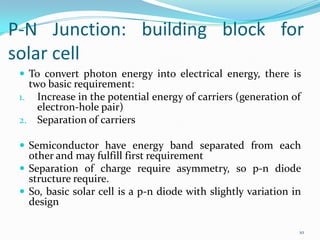
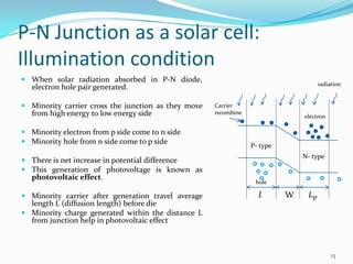
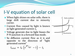
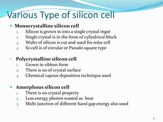
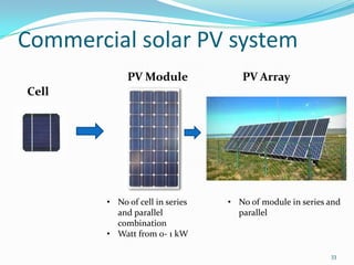
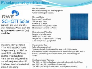
Presented By
Malik Sameeullah

NATIONAL INSTITUTE OF TECHNOLOGY,
KURUKSHETRA

1
Solar Cell

Photovoltaic (PV) Effect:
Electricity can be produced from sunlight through a
process called the PV effect, where “photo” refers to light
and “voltaic” to voltage.
Solar Cell
Solar cell is a device that converts the light energy into
electrical energy based on the principles of photovoltaic
effect.

2
Type of material: Based on
electrical conductivity
Electron energy

CB

CB

CB

overlap

Bandgap

VB

VB

metal

semiconductor

VB

insulator

Conduction band
Valance band

3
Choice of material
• Solar cell is composed of semiconductor material

• A typical silicon PV cell is composed of a thin
wafer consisting of an ultra-thin layer of
phosphorus-doped (N-type) silicon on top of a

thicker layer of boron-doped (P-type) silicon.

4
Solar Radiation: photon energy
 Solar energy is primarily transmitted to the Earth by

electromagnetic waves
 It can also be represented by particles (photons)
 Solar radiation consist of range of particles, classified
based on wavelength (frequency)

5
Region Of EM wave

Frequency

Energy

ultraviolet

100nm

1.2 keV

visible(blue)

400 nm

3.1 eV

visible(red)

700 nm

1.8 eV

infrared

10000 nm

0.12 eV

 Ultraviolet radiation is absorbed by ozone layer.
 So, solar radiation available to us have a photon energy

in between 0.1 eV to 4.4 eV
 That’s why semiconductor is used, whose band gap
energy is in between the range
 Insulator require photon of above 4.4 eV energy, so
solar radiation is not sufficient to knock electron from
valence band to conduction band
6
Fundamental of semiconductor
 Silicon and germanium are 4 group element use for








semiconductor device
Ideal semiconductor with no lattice defect and no
impurity is called an intrinsic semiconductor
Electron and holes are created in a semiconductor due
to the thermal excitation
For using it at particular temperature, impurities is
added
The process of impurity addition is called doping
The semiconductor in which impurity are added is
called extrinsic semiconductor
7
 P-type: A P-type material is one in which holes are

majority carriers i.e. they are positively charged
materials (++++)
 N-type: A N-type material is one in which electrons are
majority charge carriers i.e. they are negatively charged
materials (-----)

Fermi Level
It is the energy position within the band gap from where greater no of carriers
(holes in p type and electron in n type) get excited to become charge carrier.

For an intrinsic semiconductor , the fermi levels exists at the mid point of the
energy band.

8
P type semiconductor

Co-Valent
bonds
Si

N type semiconductor

Co-Valent
bonds

Hole

Si

In

B

Si

Si

electron

Si

Si

Si
Si

Impure atom
(donor)

Impure atom
(acceptor)

Conduction band

Electron
energy

E

Ec

Ec

Acceptor levels
Ev
Valence band

E
Eg
Ea

Electron
energy

Conduction band

Ec

Donor levels

Ec
Ed
Eg

Ev
Valence band
9
P-N Junction: building block for
solar cell
 To convert photon energy into electrical energy, there is

two basic requirement:
1. Increase in the potential energy of carriers (generation of
electron-hole pair)
2. Separation of carriers

 Semiconductor have energy band separated from each

other and may fulfill first requirement
 Separation of charge require asymmetry, so p-n diode
structure require.
 So, basic solar cell is a p-n diode with slightly variation in
design
10
P-N Junction I-V Relation
P-N junction under forward bias:
• The potential energy difference between the conduction
band at p-side and at n-side is reduced
• Majority electron diffusion current increases exponentially
with applied potential
• Minority electron drift current remain unaffected
P-N junction under reverse bias:
• Potential energy barrier height increase
• Diffusion current due to majority carrier becomes negligible
• Drift current magnitude remain as it is.
11
12
P-N Junction as a solar cell:
Illumination condition
 When solar radiation absorbed in P-N diode,
electron hole pair generated.
 Minority carrier cross the junction as they move
from high energy to low energy side
 Minority electron from p side come to n side
 Minority hole from n side come to p side
 There is net increase in potential difference
 This generation of photovoltage is known as
photovoltaic effect.
 Minority carrier after generation travel average
length L (diffusion length) before die
 Minority charge generated within the distance L
from junction help in photovoltaic effect

radiation

Carrier
recombine

electron

P- type
N- type

hole

W

13
I-V equation of solar cell


I

Dark condition

V

Illumination

14
Solar Cell Characteristics


I

V
I-V curve of solar cell and its parameter

15
Short circuit current


Band gap (eV)
Short circuit current as a function of
band gap of semiconductor materials

16
Open Circuit Voltage


17
Fill Factor


18
Efficiency
 Short circuit current decreases with increase in band





gap
Open circuit voltage increases with increase in band
gap
There is optimum band gap for maximum efficiency
The maximum solar cell efficiency of about 31% is
obtained for the optimum band gap of about 1.45 Ev
The efficiency calculate at AM1.5 and for single
junction cell

19
Losses in Solar Cell
Losses in solar
cell

Fundamental
loss
Low energy
photon

Technical loss

Electrical

Optical

Excess energy
of photon
Voltage loss
Fill Factor loss

Reflection
shadowing
Non absorbed

Ohmic

recombination

20
Spectrum Loss
 Photon having energy less than band gap energy do not

absorbed
 There is a heat loss when photon having energy higher
than band gap energy

Loss of low energy photon=23%
Loss due to excess energy of photon=33%
Maximum efficiency possible if other loss neglected=46%

21
Voltage and Fill Factor Loss
 Actual open circuit voltage is less than band gap

voltage
 Voltage loss is due to unavoidable intrinsic Auger
recombination
 For ideal solar cell FF=1
 But in actual it value is equal to 0.89
 This type of loss arises from the parasitic resistance

(series and shunt) of the cell

22
Reflection and incomplete absorption loss
 A part of radiation reflected from the cell surface
 This loss is minimized by using anti-reflective coating

and surface texturing
 Some photon have enough energy to knock carriers

 But they are not absorbed because of limited thickness

of cell

23
Top metal coverage loss
 To collect current there is metal contact network on

top
 Loss due to contact shadow is about 8%
 This loss is reduce by using transparent contact

24
Minimization of Optical Loss
 Putting anti-reflection coating on the surface
 Texturing front surface

 Minimize the front metal contact coverage area
 Making solar cell thicker to increase absorption
Anti reflection
coating

Textured
surface

25
Elementary material used in solar cell
Groups of periodic table
2nd

3rd

4th

5th

6th

B

C

Al

Si

P

S

Zn

Ga

Ge

As

Se

Cd

In

Sb

Te

Typical semiconductor used in PV cell
Elemental
• Germanium
• Silicon

Binary Compound
•
•
•
•

Ternary Compound

Gallium arsenide
Indium arsenide
Cadmium sulfide
Cadmium telluride

• Aluminium gallium arsenide

26
Commercial Silicon solar cell


27
Photovoltaic generations
Solar cell divided into three main categories called
generations:
• 1st generation: Si wafer based technology
High cost and efficient
• 2nd generation: Amorphous silicon, CdTe etc.

Low cost and less efficient
• 3rd generation: Solar Paint, bio cells

Low cost and very efficient
28
1st generation: Silicon wafer technology
2nd generation: Thin film based technology
3rd generation: Advanced nanostructure technology
29
?
1st generation

2nd generation

Silicon module

Thin film module

3rd generation
Still in research

30
Various Type of silicon cell
 Monocrystalline silicon cell
1.
Silicon is grown in into a single crystal ingot
2.
Single crystal is in the form of cylindrical block
3.
Wafer of silicon is cut and used for solar cell
4.
So cell is of circular or Pseudo square type
• Polycrystalline silicon cell
1.
Grown in ribbon form
2.
There is no of crystal surface
3.
Chemical vapour deposition technique used
 Amorphous silicon cell
1.
There is no crystal property
2.
Less energy photon wasted as heat
3.
Multi junction of different band gap energy also used
31
Monocrystalline silicon cell

Polycrystalline silicon cell
Symmetry in
structure

Circular wafer

Pseudo wafer

Square wafer
Patches in the
structure

32
Commercial solar PV system
PV Module

PV Array

Cell

• No of cell in series
and parallel
combination
• Watt from 0- 1 kW

• No of module in series and
parallel

33
Parameter of PV module


34
Test condition of module


35
PV solar panel specifications
Flexible Versions
•A variety of wiring and framing options
• are available upon request.

315 watt, 300 watt and 285
watt modules. Prices start are
$4.03/watt for cases of (20)
modules.

Independently Certified
* The ASE-270/DGF-50 is
independently certified to
meet IEEE 1262, IEC 61215
and UL 1703 standards
* It is also the only panel in
the industry to receive a UL
(Underwriters Laboratories)
Class A fire rating

Electrical Data
Power (max): 270 Watts
Voltage: 49.5 Volts
Current: 5.45 Amps
Open-circuit voltage: 60.0 Volts
Short-circuit Current: 6.1 Amps
Dimensions and Weights
Length: 74.5"/1892.3 mm
Width: 50.5"/1282.7 mm
Weight: 107 (+/- 5) lbs/46.6 (+/- 2) kg
Area: 26.13 ft sq/ 2.43 sq meters
Characteristic Data
Solar cells per panel: 216
Type of solar cell: Semi-crystalline solar cells (EFG process)
Connections: 10 AWG single conductor, stranded copper with MultiContact connector. Junction box comes with 6 built-in bypass
diodes.
Certifications and Warranty
The ASE-270-DGF/50 has been independently certified to IEC 1215
and IEEE 1262, UL 1703 (Class A Fire rating)
The ASE-270-DGF-50 comes with a 20 year power warranty.

36
PV manufacturers












Suntech Power
BP Solar
Tata BP
Moserbaer Solar
Mitbhushi Electric
GE Energy
First Solar
Sungen Solar
Bharat Electronics Limited
Kotak Urja
Sharp Solar
37
Thank
You

38

Solar pv cell

  • 1.
    Presented By Malik Sameeullah NATIONALINSTITUTE OF TECHNOLOGY, KURUKSHETRA 1
  • 2.
    Solar Cell Photovoltaic (PV)Effect: Electricity can be produced from sunlight through a process called the PV effect, where “photo” refers to light and “voltaic” to voltage. Solar Cell Solar cell is a device that converts the light energy into electrical energy based on the principles of photovoltaic effect. 2
  • 3.
    Type of material:Based on electrical conductivity Electron energy CB CB CB overlap Bandgap VB VB metal semiconductor VB insulator Conduction band Valance band 3
  • 4.
    Choice of material •Solar cell is composed of semiconductor material • A typical silicon PV cell is composed of a thin wafer consisting of an ultra-thin layer of phosphorus-doped (N-type) silicon on top of a thicker layer of boron-doped (P-type) silicon. 4
  • 5.
    Solar Radiation: photonenergy  Solar energy is primarily transmitted to the Earth by electromagnetic waves  It can also be represented by particles (photons)  Solar radiation consist of range of particles, classified based on wavelength (frequency) 5
  • 6.
    Region Of EMwave Frequency Energy ultraviolet 100nm 1.2 keV visible(blue) 400 nm 3.1 eV visible(red) 700 nm 1.8 eV infrared 10000 nm 0.12 eV  Ultraviolet radiation is absorbed by ozone layer.  So, solar radiation available to us have a photon energy in between 0.1 eV to 4.4 eV  That’s why semiconductor is used, whose band gap energy is in between the range  Insulator require photon of above 4.4 eV energy, so solar radiation is not sufficient to knock electron from valence band to conduction band 6
  • 7.
    Fundamental of semiconductor Silicon and germanium are 4 group element use for      semiconductor device Ideal semiconductor with no lattice defect and no impurity is called an intrinsic semiconductor Electron and holes are created in a semiconductor due to the thermal excitation For using it at particular temperature, impurities is added The process of impurity addition is called doping The semiconductor in which impurity are added is called extrinsic semiconductor 7
  • 8.
     P-type: AP-type material is one in which holes are majority carriers i.e. they are positively charged materials (++++)  N-type: A N-type material is one in which electrons are majority charge carriers i.e. they are negatively charged materials (-----) Fermi Level It is the energy position within the band gap from where greater no of carriers (holes in p type and electron in n type) get excited to become charge carrier. For an intrinsic semiconductor , the fermi levels exists at the mid point of the energy band. 8
  • 9.
    P type semiconductor Co-Valent bonds Si Ntype semiconductor Co-Valent bonds Hole Si In B Si Si electron Si Si Si Si Impure atom (donor) Impure atom (acceptor) Conduction band Electron energy E Ec Ec Acceptor levels Ev Valence band E Eg Ea Electron energy Conduction band Ec Donor levels Ec Ed Eg Ev Valence band 9
  • 10.
    P-N Junction: buildingblock for solar cell  To convert photon energy into electrical energy, there is two basic requirement: 1. Increase in the potential energy of carriers (generation of electron-hole pair) 2. Separation of carriers  Semiconductor have energy band separated from each other and may fulfill first requirement  Separation of charge require asymmetry, so p-n diode structure require.  So, basic solar cell is a p-n diode with slightly variation in design 10
  • 11.
    P-N Junction I-VRelation P-N junction under forward bias: • The potential energy difference between the conduction band at p-side and at n-side is reduced • Majority electron diffusion current increases exponentially with applied potential • Minority electron drift current remain unaffected P-N junction under reverse bias: • Potential energy barrier height increase • Diffusion current due to majority carrier becomes negligible • Drift current magnitude remain as it is. 11
  • 12.
  • 13.
    P-N Junction asa solar cell: Illumination condition  When solar radiation absorbed in P-N diode, electron hole pair generated.  Minority carrier cross the junction as they move from high energy to low energy side  Minority electron from p side come to n side  Minority hole from n side come to p side  There is net increase in potential difference  This generation of photovoltage is known as photovoltaic effect.  Minority carrier after generation travel average length L (diffusion length) before die  Minority charge generated within the distance L from junction help in photovoltaic effect radiation Carrier recombine electron P- type N- type hole W 13
  • 14.
    I-V equation ofsolar cell  I Dark condition V Illumination 14
  • 15.
    Solar Cell Characteristics  I V I-Vcurve of solar cell and its parameter 15
  • 16.
    Short circuit current  Bandgap (eV) Short circuit current as a function of band gap of semiconductor materials 16
  • 17.
  • 18.
  • 19.
    Efficiency  Short circuitcurrent decreases with increase in band     gap Open circuit voltage increases with increase in band gap There is optimum band gap for maximum efficiency The maximum solar cell efficiency of about 31% is obtained for the optimum band gap of about 1.45 Ev The efficiency calculate at AM1.5 and for single junction cell 19
  • 20.
    Losses in SolarCell Losses in solar cell Fundamental loss Low energy photon Technical loss Electrical Optical Excess energy of photon Voltage loss Fill Factor loss Reflection shadowing Non absorbed Ohmic recombination 20
  • 21.
    Spectrum Loss  Photonhaving energy less than band gap energy do not absorbed  There is a heat loss when photon having energy higher than band gap energy Loss of low energy photon=23% Loss due to excess energy of photon=33% Maximum efficiency possible if other loss neglected=46% 21
  • 22.
    Voltage and FillFactor Loss  Actual open circuit voltage is less than band gap voltage  Voltage loss is due to unavoidable intrinsic Auger recombination  For ideal solar cell FF=1  But in actual it value is equal to 0.89  This type of loss arises from the parasitic resistance (series and shunt) of the cell 22
  • 23.
    Reflection and incompleteabsorption loss  A part of radiation reflected from the cell surface  This loss is minimized by using anti-reflective coating and surface texturing  Some photon have enough energy to knock carriers  But they are not absorbed because of limited thickness of cell 23
  • 24.
    Top metal coverageloss  To collect current there is metal contact network on top  Loss due to contact shadow is about 8%  This loss is reduce by using transparent contact 24
  • 25.
    Minimization of OpticalLoss  Putting anti-reflection coating on the surface  Texturing front surface  Minimize the front metal contact coverage area  Making solar cell thicker to increase absorption Anti reflection coating Textured surface 25
  • 26.
    Elementary material usedin solar cell Groups of periodic table 2nd 3rd 4th 5th 6th B C Al Si P S Zn Ga Ge As Se Cd In Sb Te Typical semiconductor used in PV cell Elemental • Germanium • Silicon Binary Compound • • • • Ternary Compound Gallium arsenide Indium arsenide Cadmium sulfide Cadmium telluride • Aluminium gallium arsenide 26
  • 27.
  • 28.
    Photovoltaic generations Solar celldivided into three main categories called generations: • 1st generation: Si wafer based technology High cost and efficient • 2nd generation: Amorphous silicon, CdTe etc. Low cost and less efficient • 3rd generation: Solar Paint, bio cells Low cost and very efficient 28
  • 29.
    1st generation: Siliconwafer technology 2nd generation: Thin film based technology 3rd generation: Advanced nanostructure technology 29
  • 30.
    ? 1st generation 2nd generation Siliconmodule Thin film module 3rd generation Still in research 30
  • 31.
    Various Type ofsilicon cell  Monocrystalline silicon cell 1. Silicon is grown in into a single crystal ingot 2. Single crystal is in the form of cylindrical block 3. Wafer of silicon is cut and used for solar cell 4. So cell is of circular or Pseudo square type • Polycrystalline silicon cell 1. Grown in ribbon form 2. There is no of crystal surface 3. Chemical vapour deposition technique used  Amorphous silicon cell 1. There is no crystal property 2. Less energy photon wasted as heat 3. Multi junction of different band gap energy also used 31
  • 32.
    Monocrystalline silicon cell Polycrystallinesilicon cell Symmetry in structure Circular wafer Pseudo wafer Square wafer Patches in the structure 32
  • 33.
    Commercial solar PVsystem PV Module PV Array Cell • No of cell in series and parallel combination • Watt from 0- 1 kW • No of module in series and parallel 33
  • 34.
    Parameter of PVmodule  34
  • 35.
    Test condition ofmodule  35
  • 36.
    PV solar panelspecifications Flexible Versions •A variety of wiring and framing options • are available upon request. 315 watt, 300 watt and 285 watt modules. Prices start are $4.03/watt for cases of (20) modules. Independently Certified * The ASE-270/DGF-50 is independently certified to meet IEEE 1262, IEC 61215 and UL 1703 standards * It is also the only panel in the industry to receive a UL (Underwriters Laboratories) Class A fire rating Electrical Data Power (max): 270 Watts Voltage: 49.5 Volts Current: 5.45 Amps Open-circuit voltage: 60.0 Volts Short-circuit Current: 6.1 Amps Dimensions and Weights Length: 74.5"/1892.3 mm Width: 50.5"/1282.7 mm Weight: 107 (+/- 5) lbs/46.6 (+/- 2) kg Area: 26.13 ft sq/ 2.43 sq meters Characteristic Data Solar cells per panel: 216 Type of solar cell: Semi-crystalline solar cells (EFG process) Connections: 10 AWG single conductor, stranded copper with MultiContact connector. Junction box comes with 6 built-in bypass diodes. Certifications and Warranty The ASE-270-DGF/50 has been independently certified to IEC 1215 and IEEE 1262, UL 1703 (Class A Fire rating) The ASE-270-DGF-50 comes with a 20 year power warranty. 36
  • 37.
    PV manufacturers            Suntech Power BPSolar Tata BP Moserbaer Solar Mitbhushi Electric GE Energy First Solar Sungen Solar Bharat Electronics Limited Kotak Urja Sharp Solar 37
  • 38.