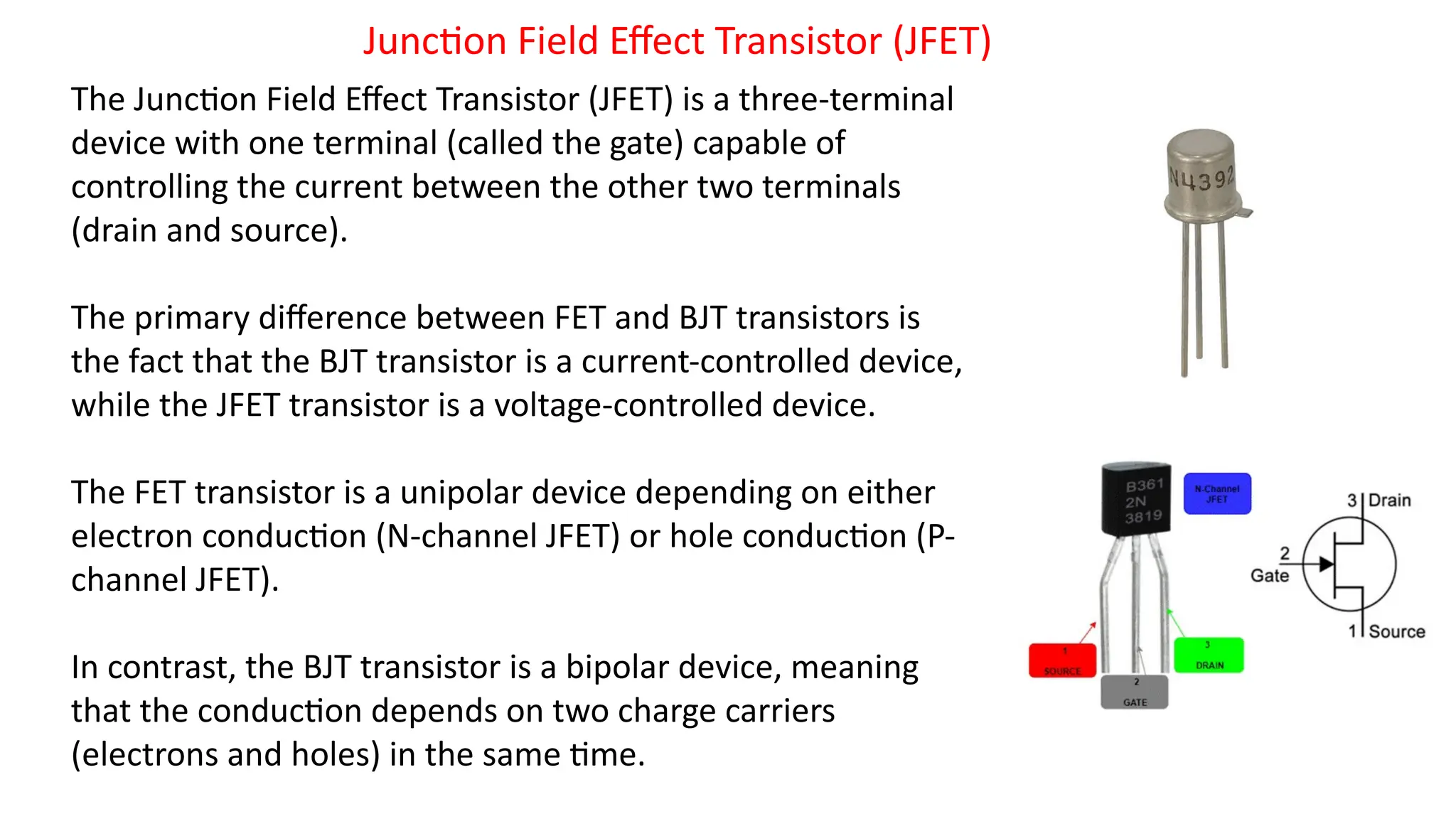
The Junction FieldEffect Transistor (JFET) is a three-terminal
device with one terminal (called the gate) capable of
controlling the current between the other two terminals
(drain and source).
The primary difference between FET and BJT transistors is
the fact that the BJT transistor is a current-controlled device,
while the JFET transistor is a voltage-controlled device.
The FET transistor is a unipolar device depending on either
electron conduction (N-channel JFET) or hole conduction (P-
channel JFET).
In contrast, the BJT transistor is a bipolar device, meaning
that the conduction depends on two charge carriers
(electrons and holes) in the same time.
Junction Field Effect Transistor (JFET)
3.
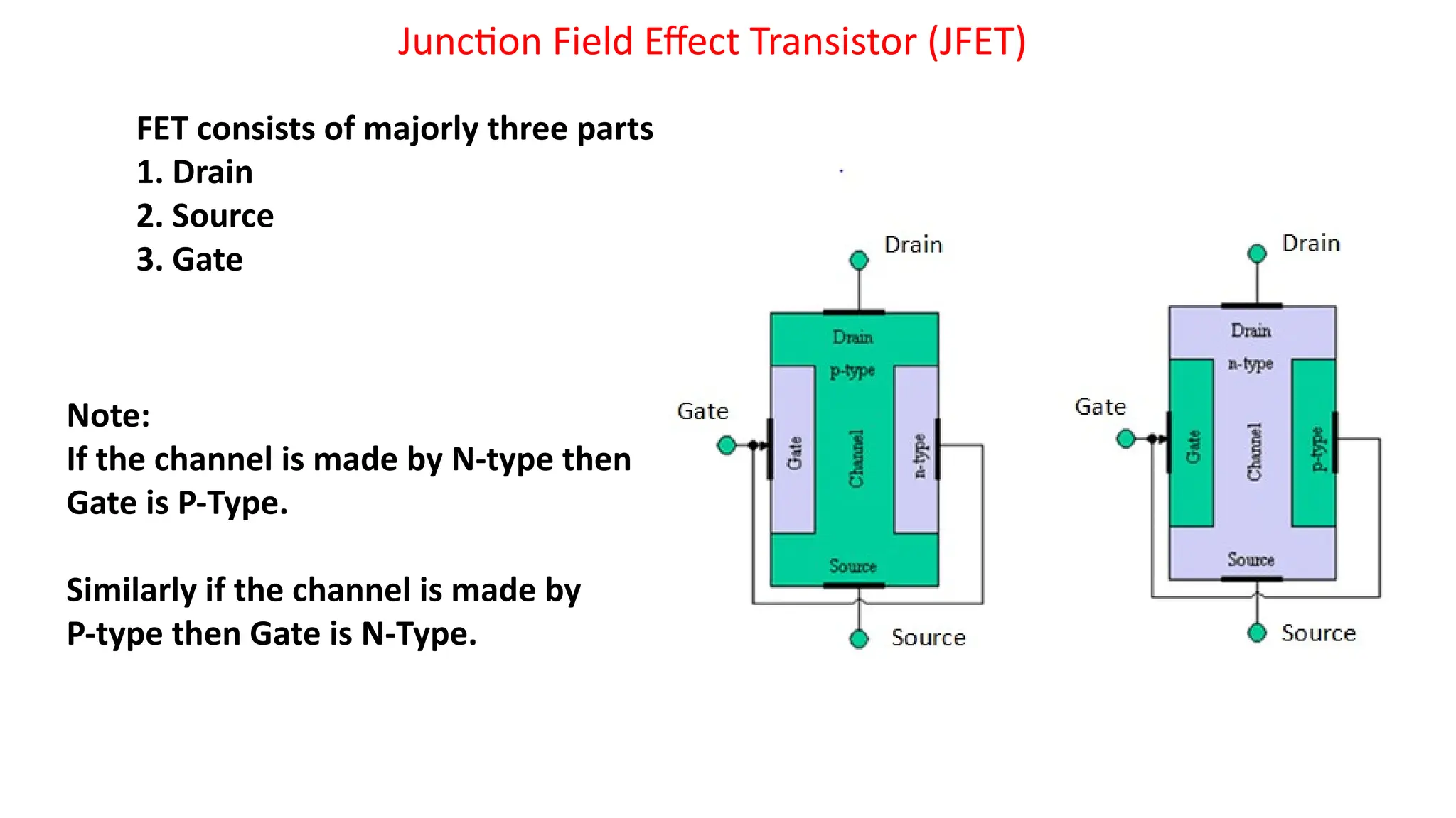
FET consists ofmajorly three parts
1. Drain
2. Source
3. Gate
Junction Field Effect Transistor (JFET)
Note:
If the channel is made by N-type then
Gate is P-Type.
Similarly if the channel is made by
P-type then Gate is N-Type.
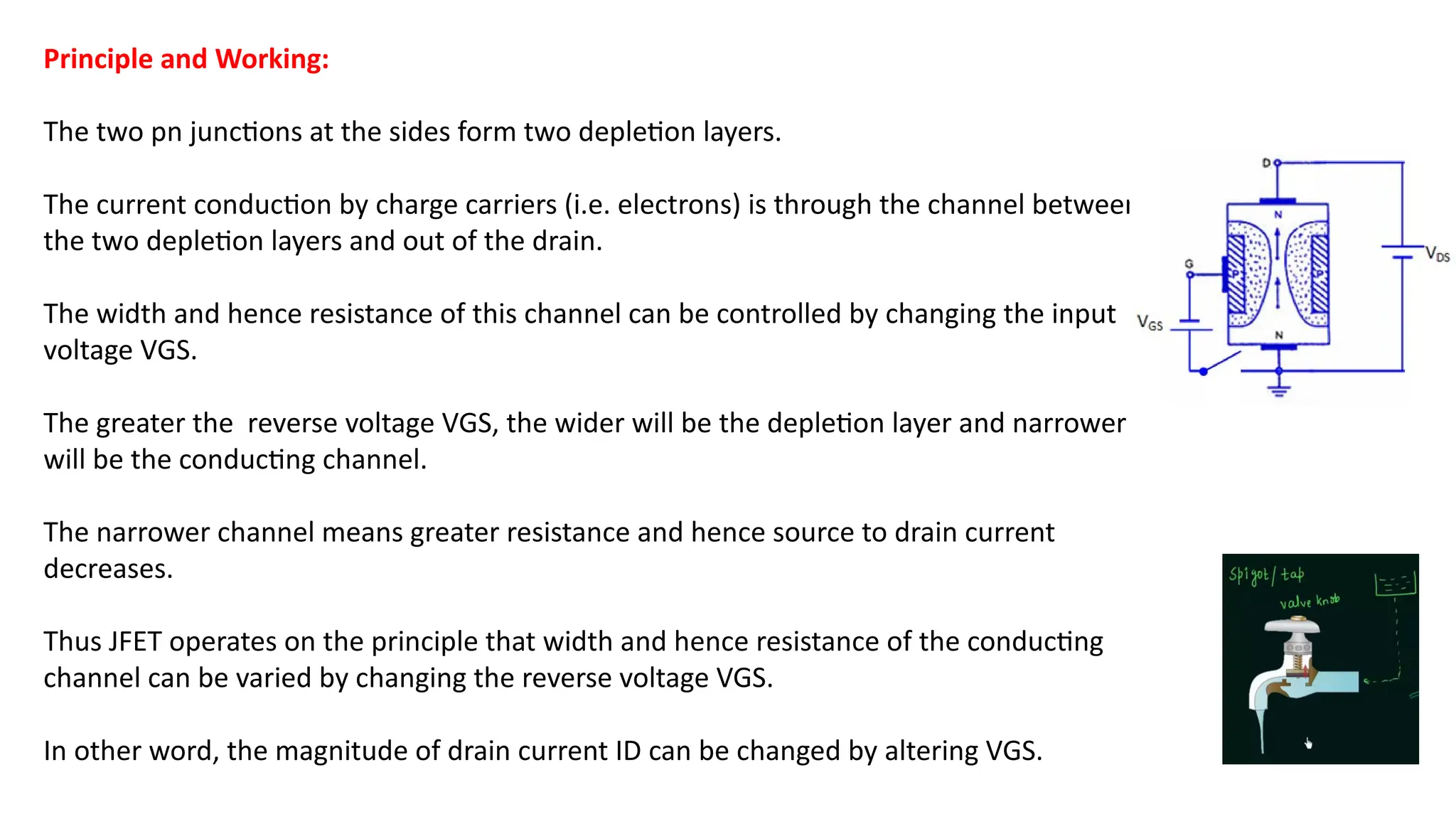
Principle and Working:
Thetwo pn junctions at the sides form two depletion layers.
The current conduction by charge carriers (i.e. electrons) is through the channel between
the two depletion layers and out of the drain.
The width and hence resistance of this channel can be controlled by changing the input
voltage VGS.
The greater the reverse voltage VGS, the wider will be the depletion layer and narrower
will be the conducting channel.
The narrower channel means greater resistance and hence source to drain current
decreases.
Thus JFET operates on the principle that width and hence resistance of the conducting
channel can be varied by changing the reverse voltage VGS.
In other word, the magnitude of drain current ID can be changed by altering VGS.
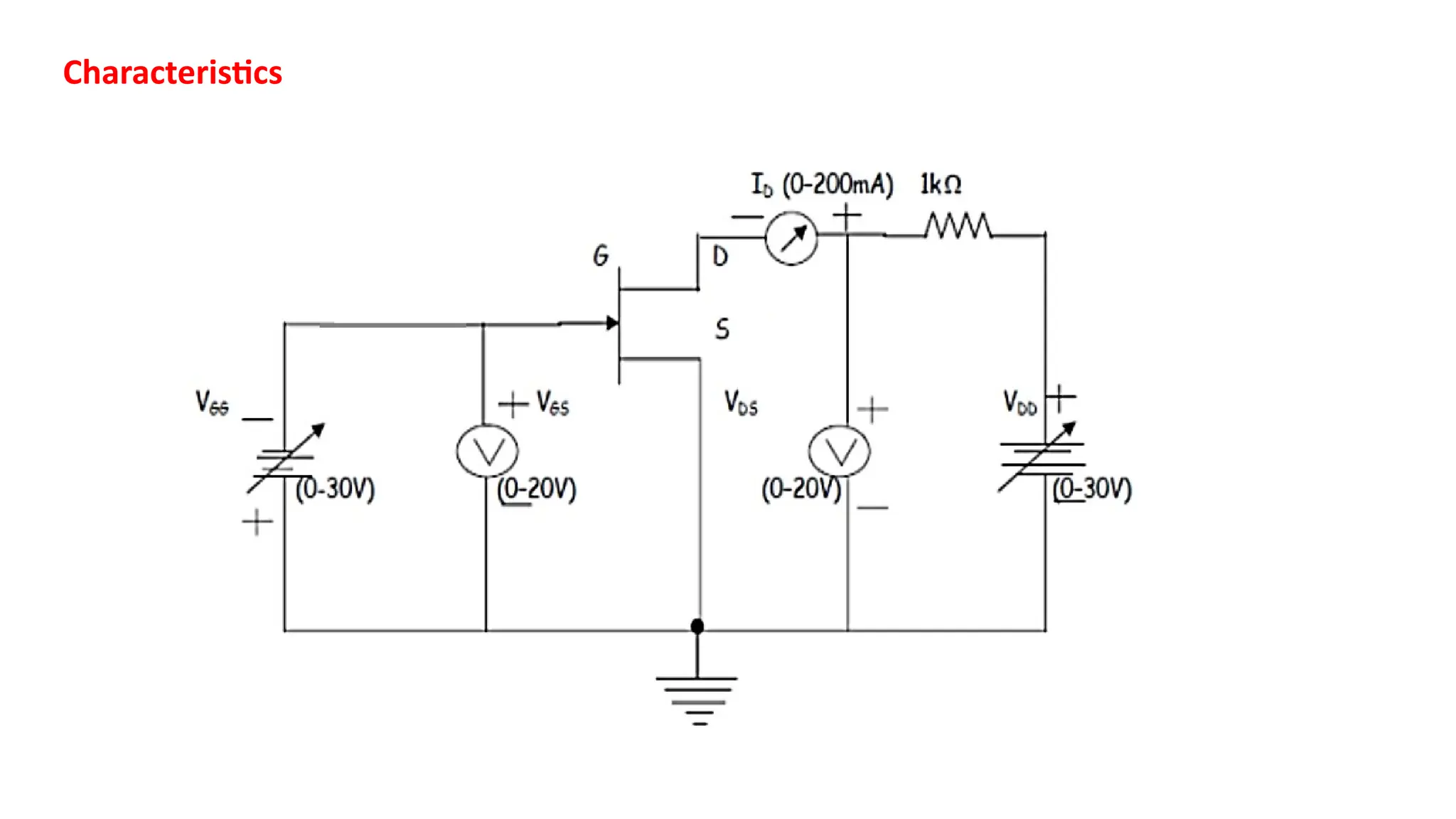
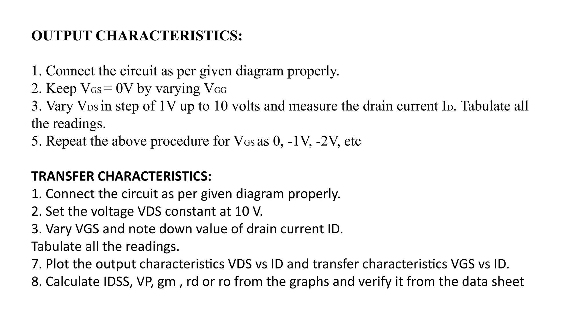
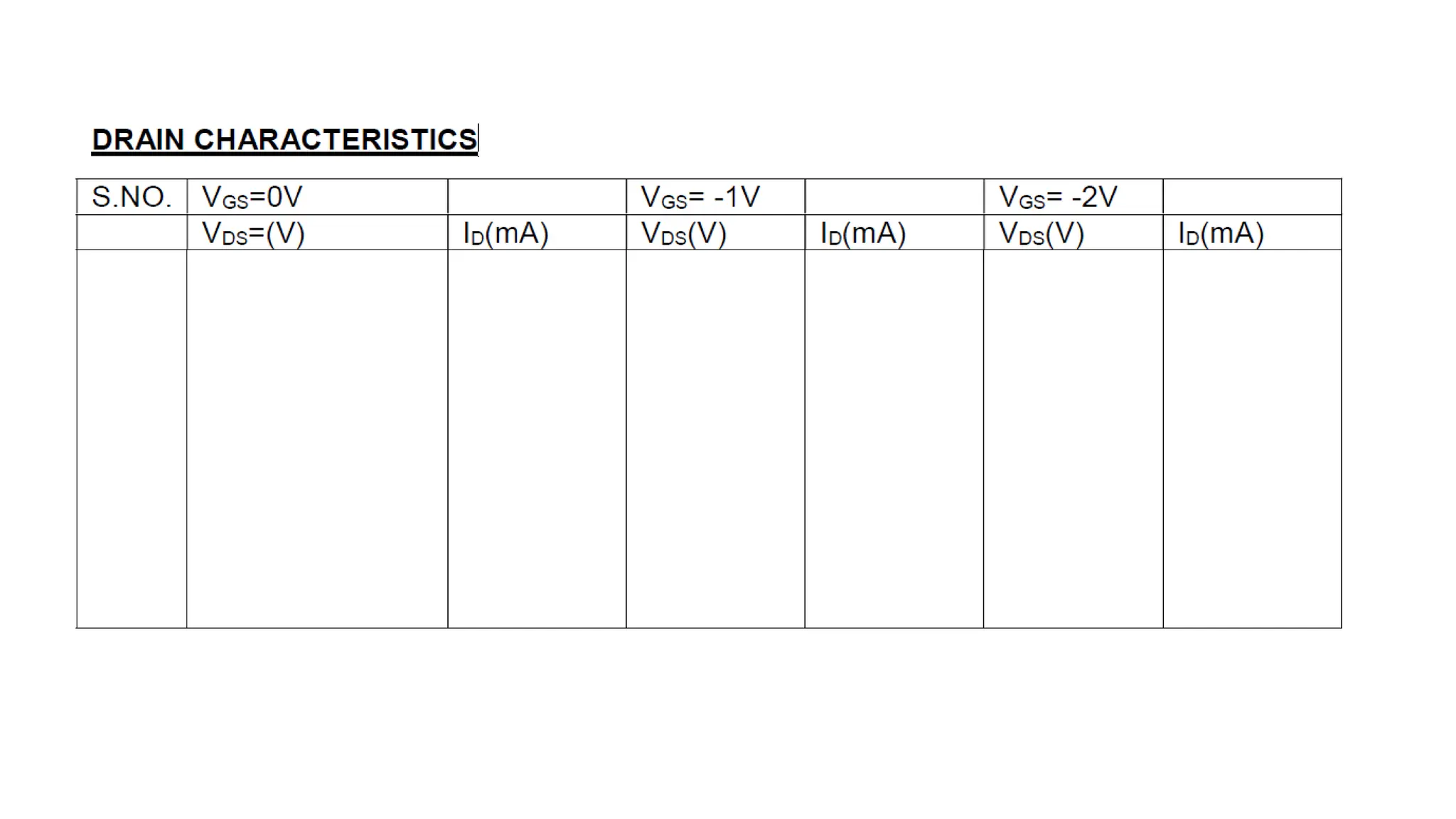
OUTPUT CHARACTERISTICS:
1. Connectthe circuit as per given diagram properly.
2. Keep VGS = 0V by varying VGG
3. Vary VDS in step of 1V up to 10 volts and measure the drain current ID. Tabulate all
the readings.
5. Repeat the above procedure for VGS as 0, -1V, -2V, etc
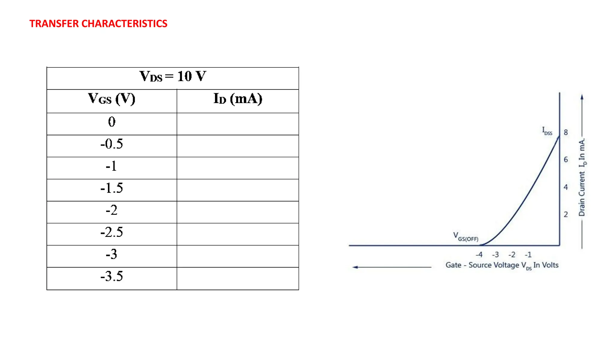
TRANSFER CHARACTERISTICS:
1. Connect the circuit as per given diagram properly.
2. Set the voltage VDS constant at 10 V.
3. Vary VGS and note down value of drain current ID.
Tabulate all the readings.
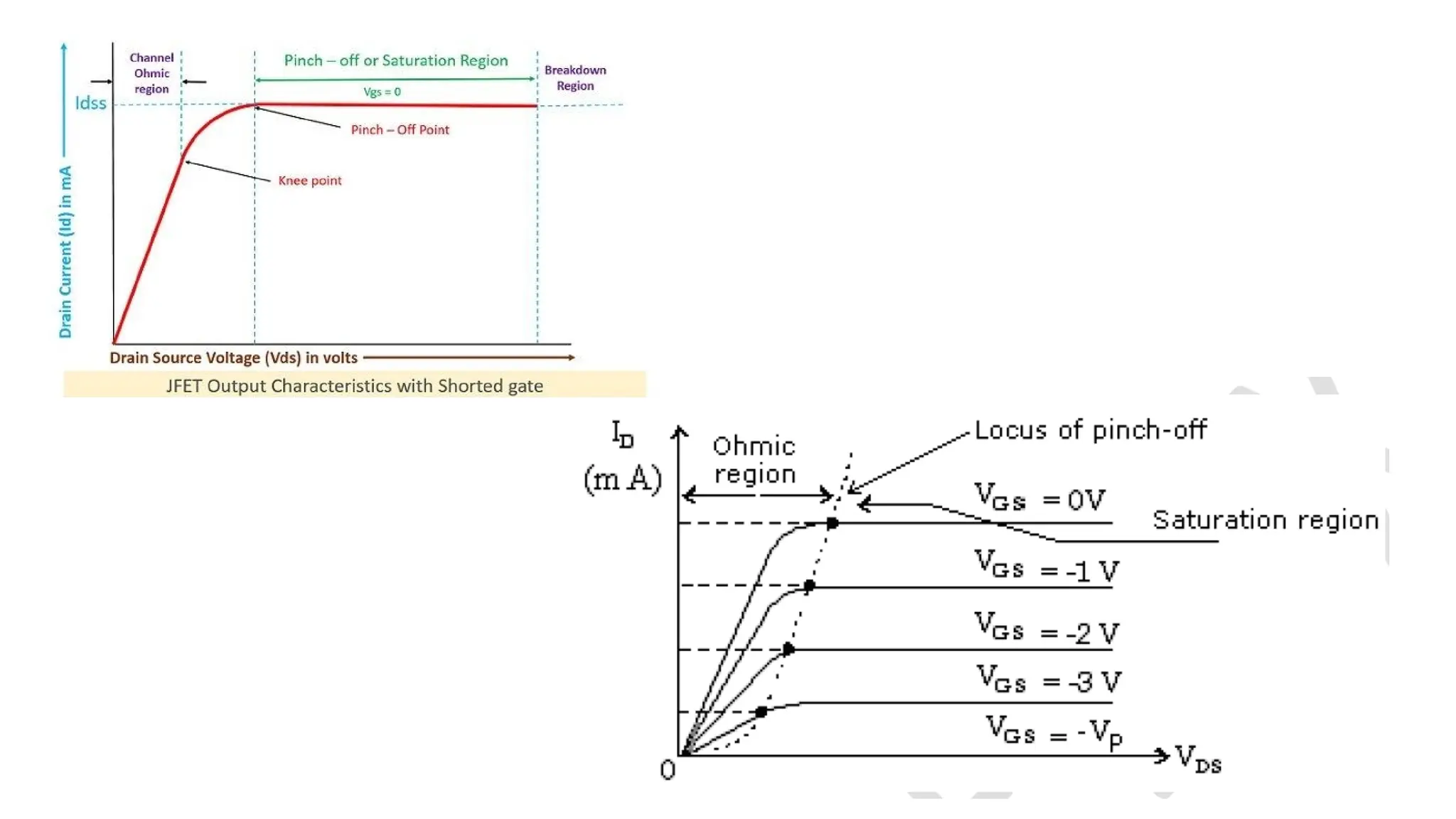
7. Plot the output characteristics VDS vs ID and transfer characteristics VGS vs ID.
8. Calculate IDSS, VP, gm , rd or ro from the graphs and verify it from the data sheet
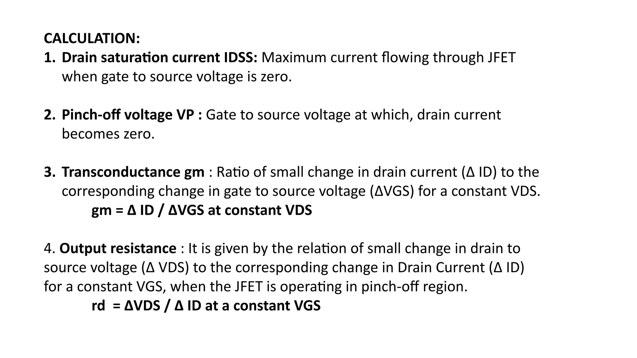
CALCULATION:
1. Drain saturationcurrent IDSS: Maximum current flowing through JFET
when gate to source voltage is zero.
2. Pinch-off voltage VP : Gate to source voltage at which, drain current
becomes zero.
3. Transconductance gm : Ratio of small change in drain current (Δ ID) to the
corresponding change in gate to source voltage (ΔVGS) for a constant VDS.
gm = Δ ID / ΔVGS at constant VDS
4. Output resistance : It is given by the relation of small change in drain to
source voltage (Δ VDS) to the corresponding change in Drain Current (Δ ID)
for a constant VGS, when the JFET is operating in pinch-off region.
rd = ΔVDS / Δ ID at a constant VGS


![Aim-to study characterstics of fet (field effect [Autosaved].pptx](https://cdn.slidesharecdn.com/ss_thumbnails/aim-tostudycharactersticsoffetfieldeffectautosaved-221113041420-4dcee974-thumbnail.jpg?width=640&height=640&fit=bounds)


