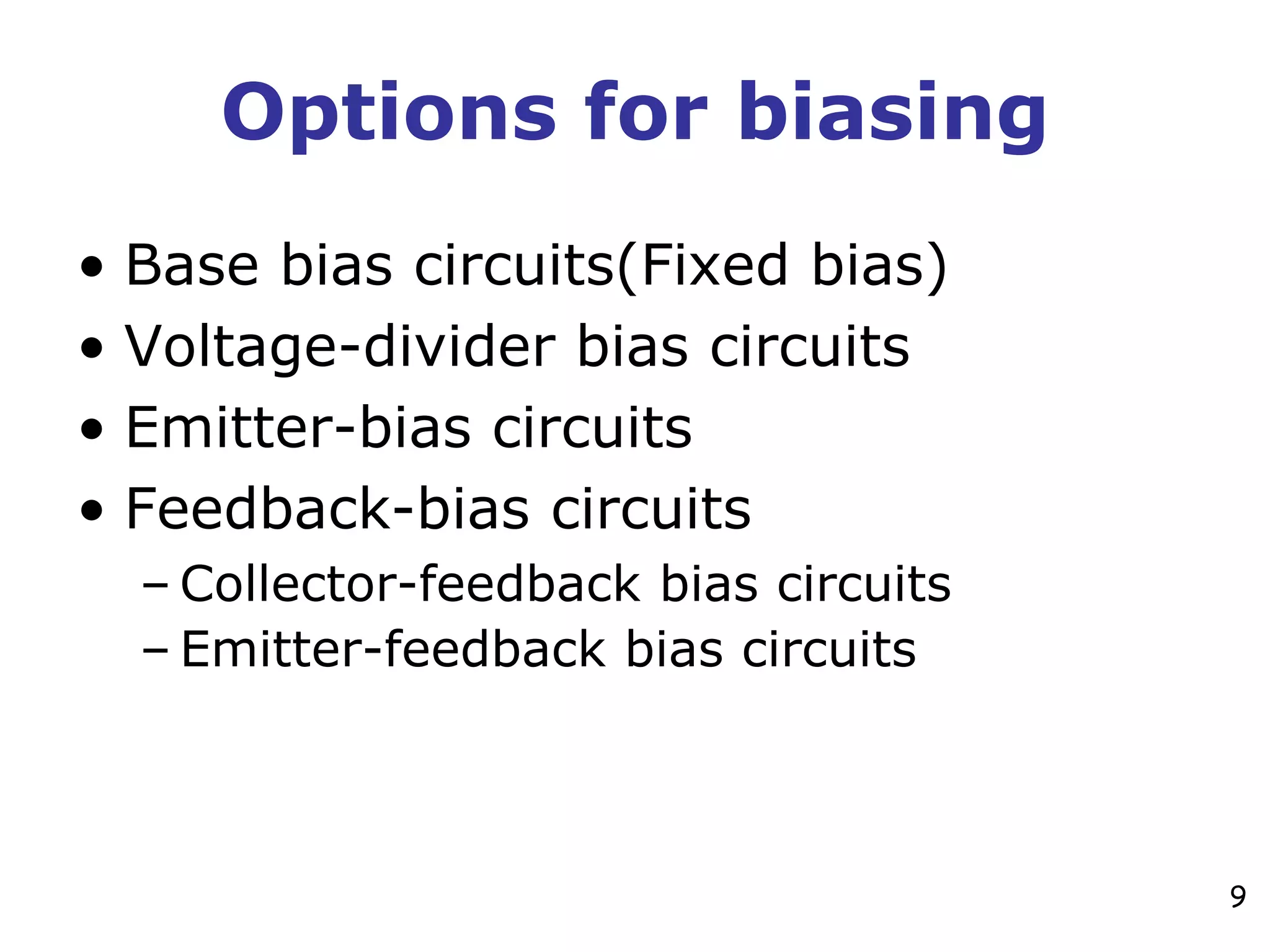
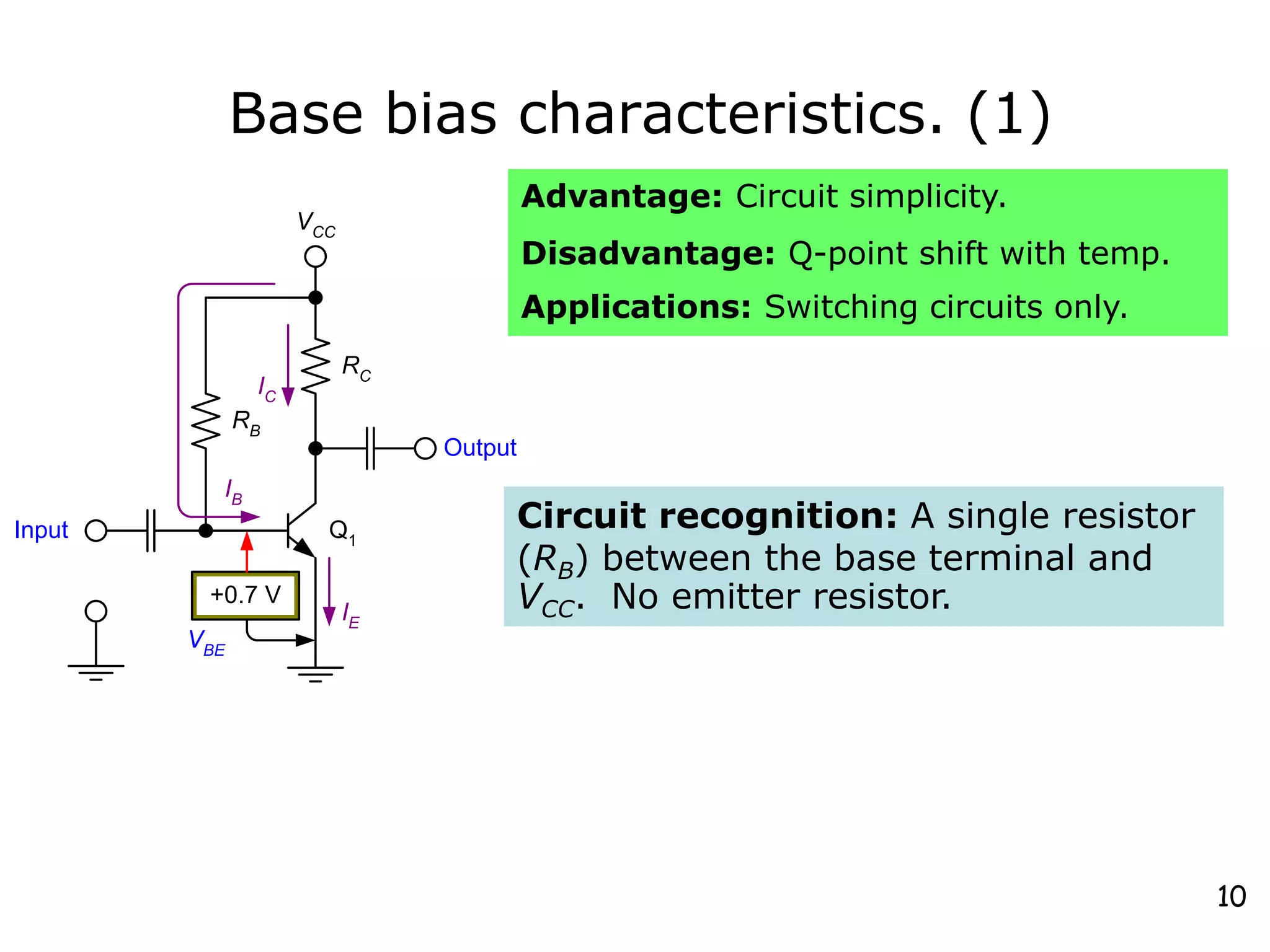
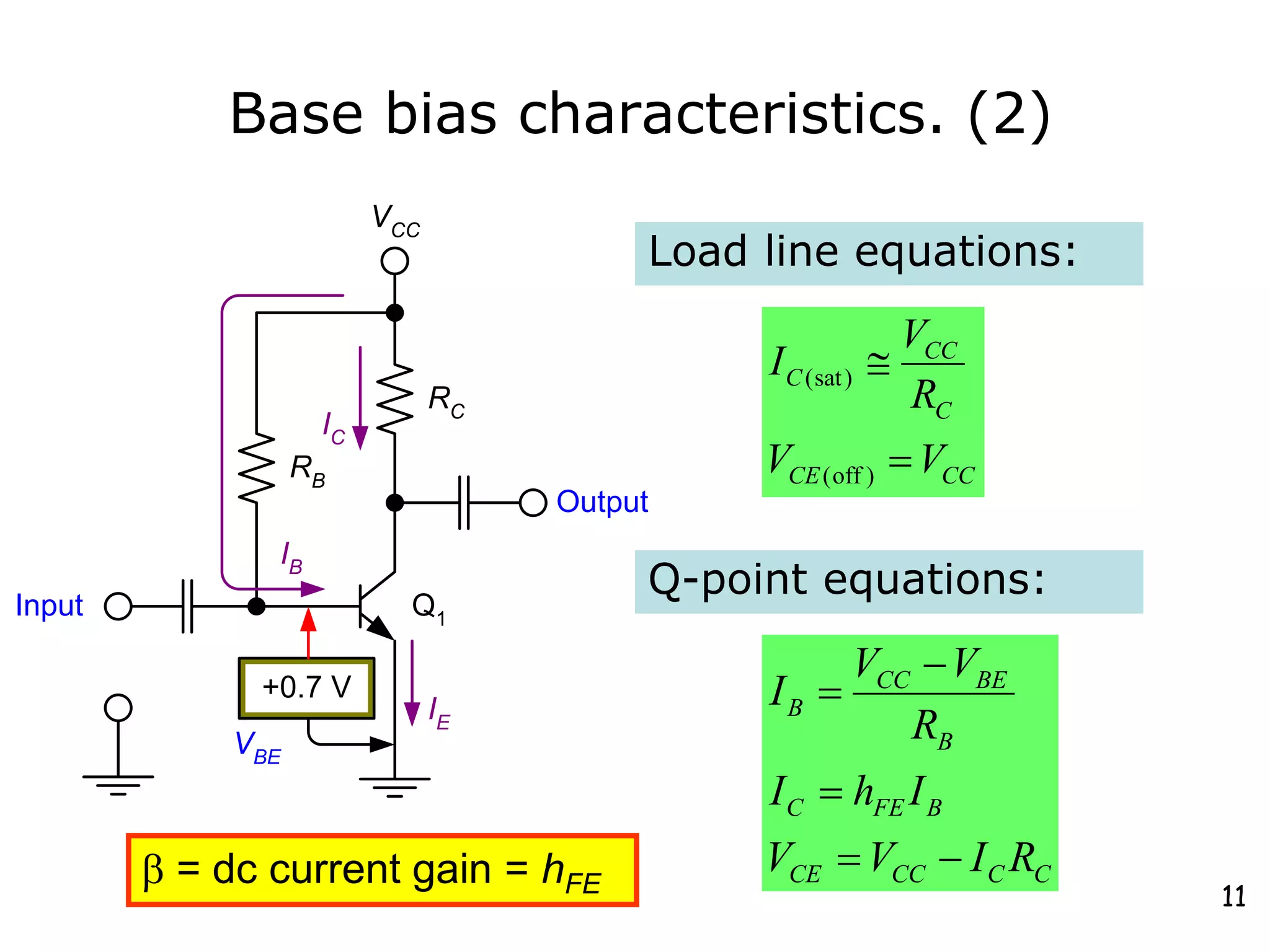
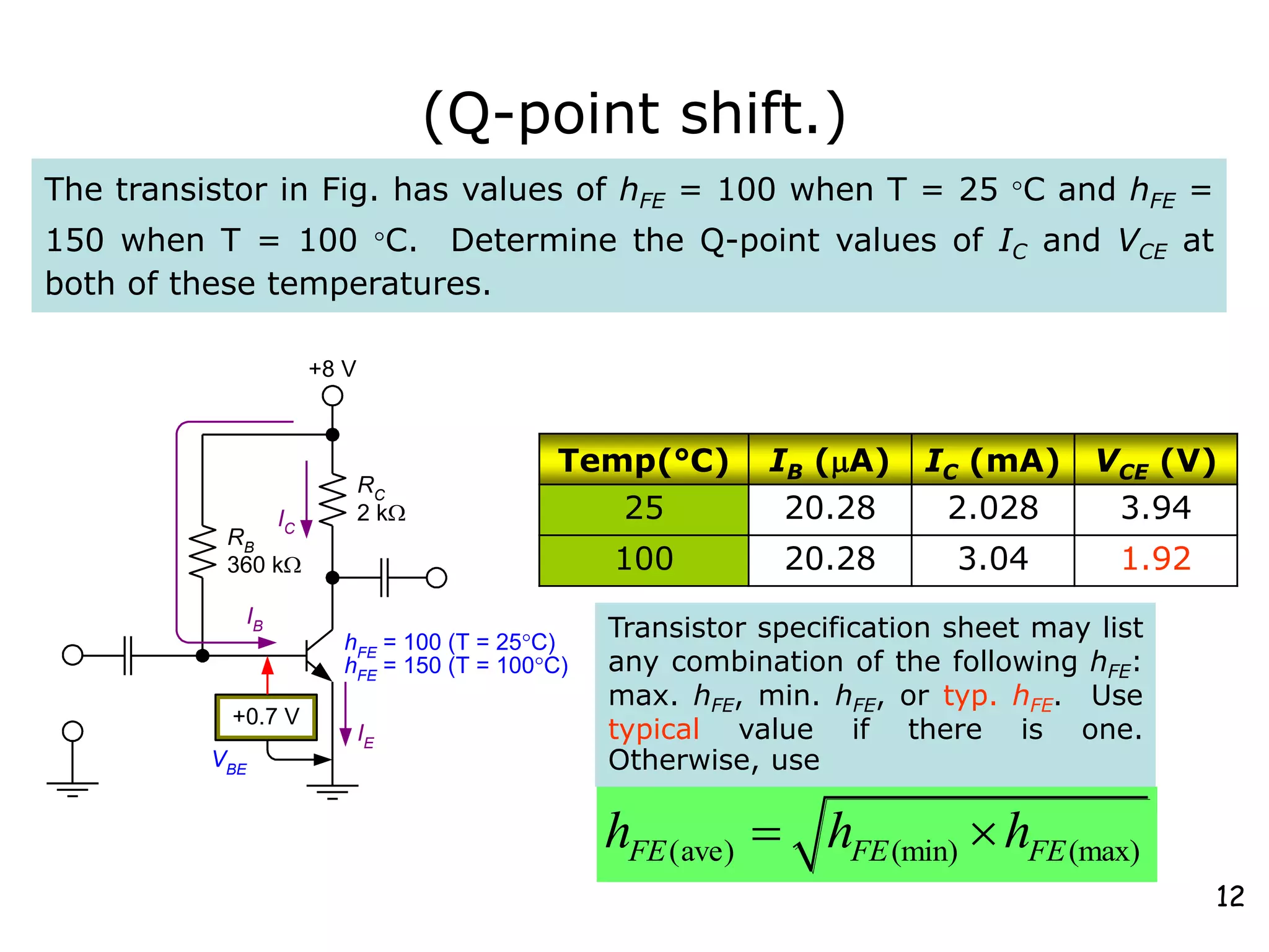
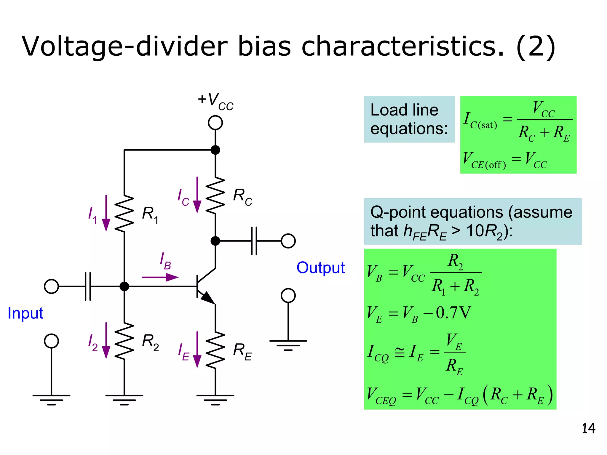
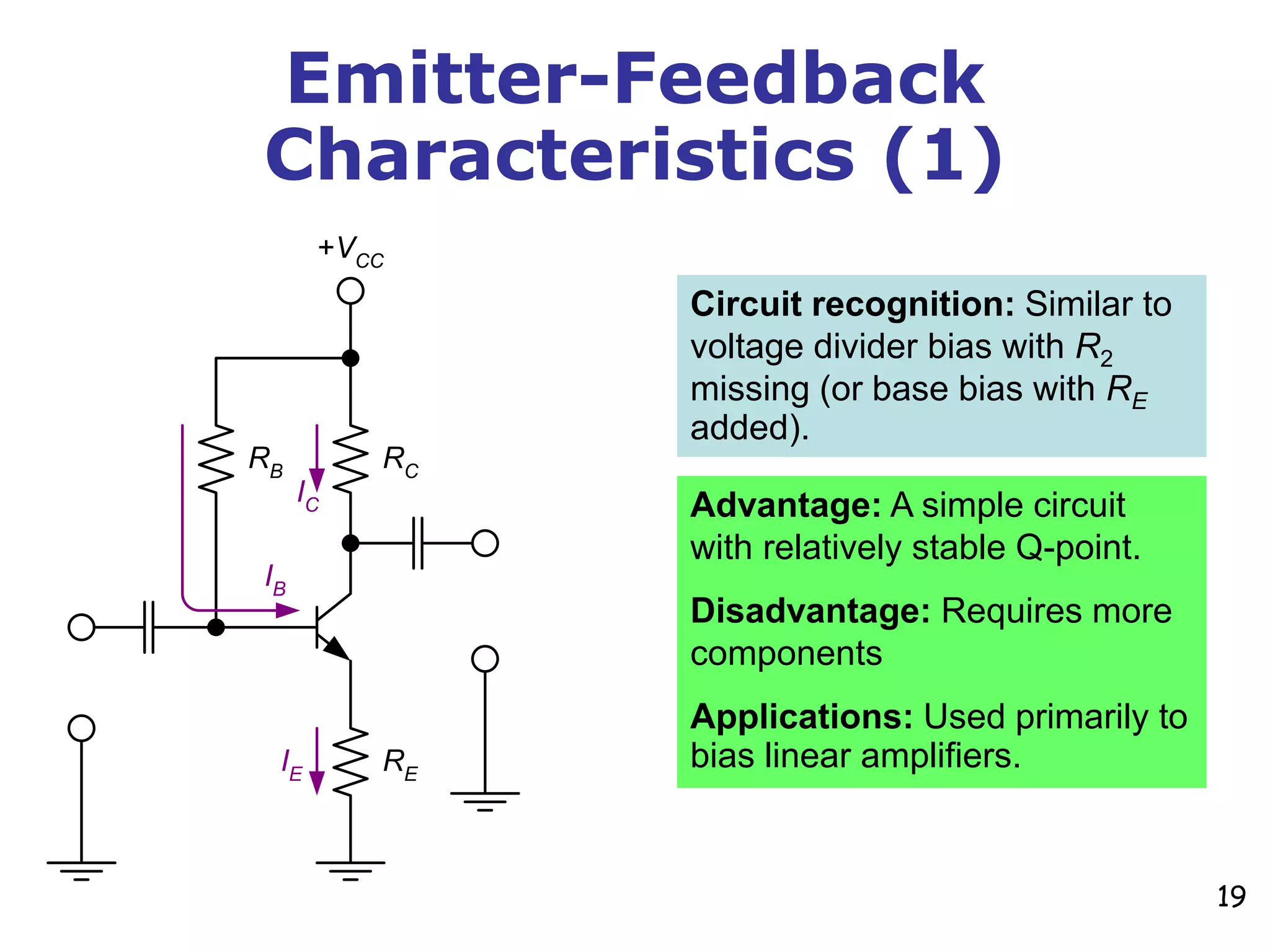
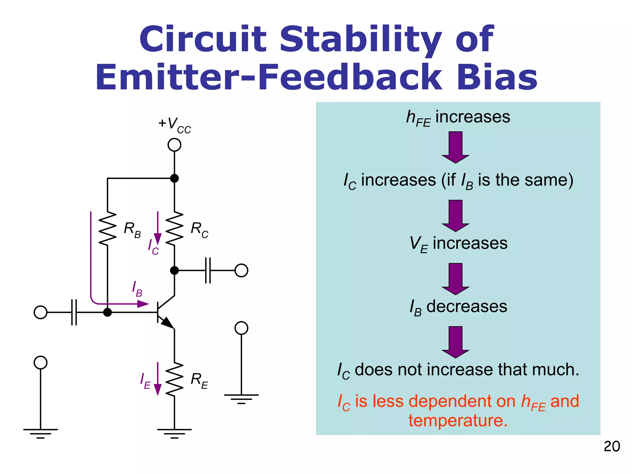
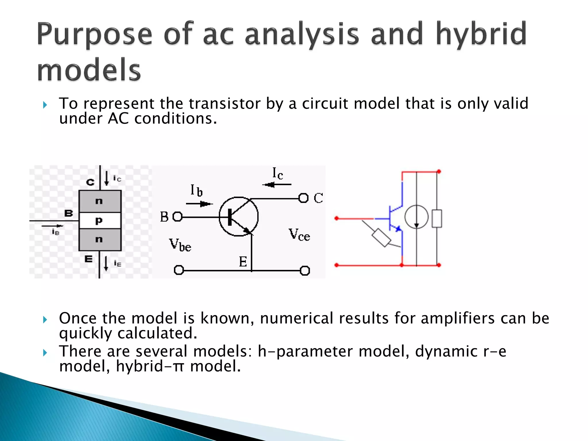
1. The document discusses various transistor amplifier circuit designs and analysis techniques, including biasing circuits like base bias, voltage divider bias, and emitter feedback bias.
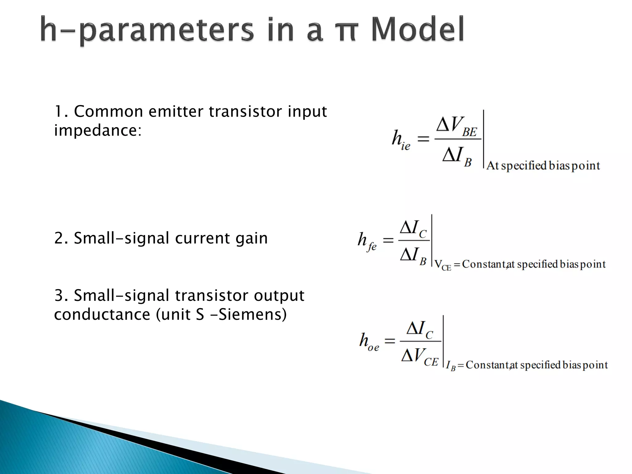
2. It introduces the small-signal h-parameter transistor model that represents the transistor under AC conditions and defines terms like small-signal current gain and output conductance.
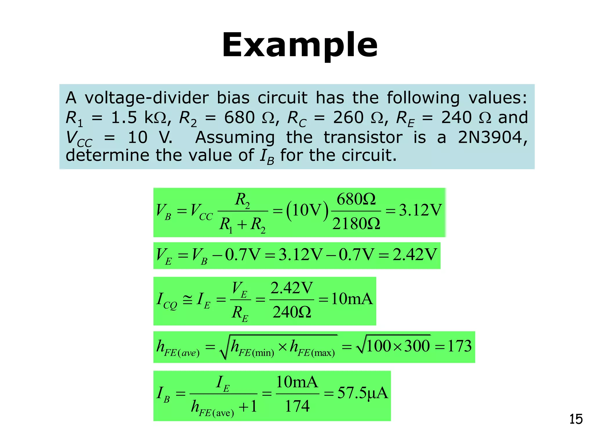
3. The document provides examples of calculating Q-points, load lines, and biasing component values for different transistor amplifier circuits.


![Transformer Repair Workshop Report [EEE]](https://cdn.slidesharecdn.com/ss_thumbnails/transformerrepairworkshopeee-140621072318-phpapp01-thumbnail.jpg?width=640&height=640&fit=bounds)


![Bipolar Junction Transistor Biasing [Types]](https://cdn.slidesharecdn.com/ss_thumbnails/ele307module2working-1-251030220651-e41b5c93-thumbnail.jpg?width=640&height=640&fit=bounds)