Downloaded 271 times


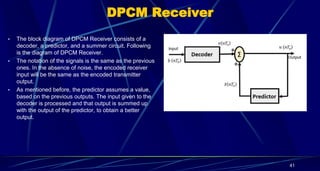
![• The predictor produces the assumed samples from the previous outputs of the
transmitter circuit. The input to this predictor is the quantized versions of the input
signal x(nTs).
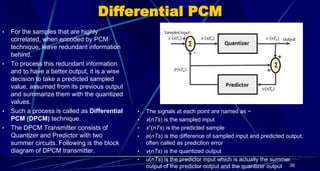
• Quantizer Output is represented as −
• v(nTs)=Q[e(nTs)]
• =e(nTs)+q(nTs)
• Where q (nTs) is the quantization error
• Predictor input is the sum of quantizer output and predictor output,
• u(nTs)=xˆ(nTs)+v(nTs)
• u(nTs)=xˆ(nTs)+e(nTs)+q(nTs)
• u(nTs)=x(nTs)+q(nTs)
• The same predictor circuit is used in the decoder to reconstruct the original input.
40](https://image.slidesharecdn.com/ec6651communicationengineeringunit2-171212164018/85/EC6651-COMMUNICATION-ENGINEERING-UNIT-2-40-320.jpg)


The document covers key concepts in digital communication, focusing on pulse modulation techniques including pulse amplitude modulation (PAM), pulse width modulation (PWM), and pulse position modulation (PPM), as well as the principles of sampling and quantization. It explains the advantages of digital signals over analog signals, such as better noise immunity and recovery capabilities. The document also discusses the Nyquist theorem, quantization error, and various encoding techniques used in digital communication systems.