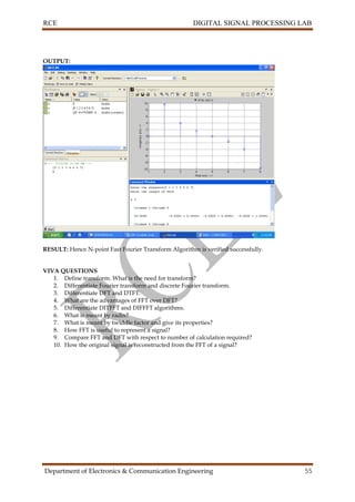
This document provides information about a digital signal processing laboratory manual, including:
- An index listing 12 experiments covering topics like DSP chip architecture, linear and circular convolution, FIR and IIR filter design, FFT implementation, frequency response analysis, and power spectral density computation.
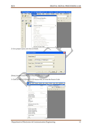
- General instructions for successfully completing experiments within the 3-hour laboratory period and guidance for laboratory reports.
- Procedures for working with MATLAB and Code Composer Studio software to execute experiments and programs on a DSP processor.
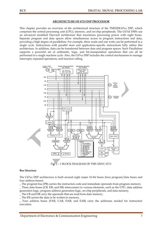
- An introduction to digital signal processors and an overview of the architecture of the TMS320C67xx DSP chip used, including its CPU, memory, peripherals, and advanced parallel processing capabilities
![RCE DIGITAL SIGNAL PROCESSING LAB
Department of Electronics & Communication Engineering 4
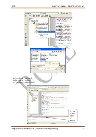
WORKING PROCEDURE WITH MATLAB:
1) Double click on Matlab icon. -> Then Matlab will be opened
2) To write the Matlab Program Goto file menu-> New -> Script(Mfile) -> In the opened
Script file write the Matlab code and save the file with an extension of .m
Ex: “linear.m”
3)To execute Matlab Program Select the all lines in matlab program(ctrl+A) of mfile and press “F9”
to execute the matlab code
4)Entering the inputs in command window
If the command window is displaying the message like “enter the input sequence” then
enter the sequence with square brackets and each sample values is spaced with single
space
Ex: Enter input sequence [1 2 3 4]
If it is asking a value input write the value without brackets
Ex: “enter length of sequence 4”
After entering inputs It displays the Output Graphs.
PROCEDURE TO WORK ON CODE COMPOSER STUDIO
PROCEDURE FOR EXECUTING NON REAL TIME PROGRAMS
(EX: LINEAR & CIRCULAR CONVOLUTION, FFT, PSD)
Test the USB port by running DSK Port test from the start menu
Use StartProgramsTexas InstrumentsCode Composer StudioCode Composer Studio
CDSK6713 Tools DSK6713 Diagnostic Utilities
Select StartSelect DSK6713 Diagnostic Utility Icon from Desktop
Select Start Option
Utility Program will test the board
After testing Diagnostic Status you will get PASS
To create the New Project
Project New (File Name. pjt , Eg: Vectors.pjt)
To Create a Source file
File New Type the code (Save & give file name, Eg: sum.c).
To Add Source files to Project
Project Add files to Project c/ccs studio3.1/my projects/your project name/
sum.c(select the file type as c/c++ source files)
To Add rts.lib file & hello.cmd:
Project Add files to Project rts6700.lib
(Path:c/ccs studio3.1/cg tools/c6000/lib/ rts6700.lib)
Note: Select Object & Library in(*.o,*.l) in Type of files
Project Add files to Project hello.cmd
CMD file – Which is common for all non real time programs.
(Path: c/ccs studio3.1tutorialdsk 6713 hello1hello.cmd)
Note: Select Linker Command file(*.cmd) in Type of files
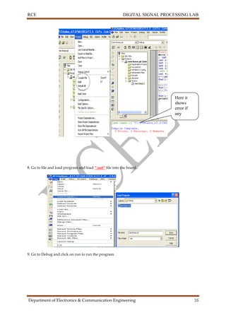
Compile:
To Compile: Project Compile project
To Build: Project build project,
To Rebuild: Project rebuild,
Which will create the final .out executable file.(Eg. Vectors.out).](https://image.slidesharecdn.com/dsplabmanual15-11-2016-190215035806/85/Dsp-lab-manual-15-11-2016-4-320.jpg)
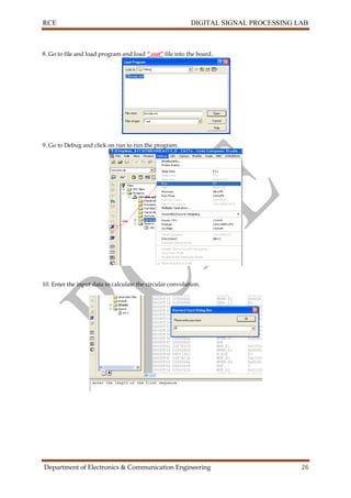
![RCE DIGITAL SIGNAL PROCESSING LAB
Department of Electronics & Communication Engineering 5
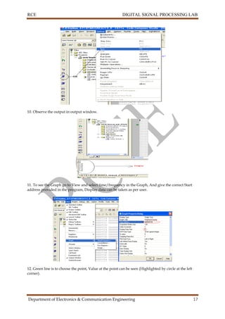
Procedure to Load and Run program:
Load the program to DSK: File Load program Vectors. out
To Execute project: Debug Run.
1. Execution should halt at break point.
2. Now press F10. See the changes happening in the watch window.
3. Similarly go to view & select CPU registers to view the changes happening in CPU registers.
Configure the graphical window as shown below
INPUT
x[n] = {1, 2, 3, 4,0,0,0,0}
h[k] = {1, 2, 3, 4,0,0,0,0}
OUTPUT:
b)PROCEDURE FOR EXECUTING REAL TIME PROGRAMS
(EX:IIR FILTERS,FIR FILTERS DESIGNING)
CONNECTING DSP PROCESSOR TO PC
Connect the dsp processor to the pc using usb cable connector.
Check the DSK6713 diagnostics (IF you get the “pass”then click on ok).
Click on ccs studio3.1 desktop icon. Then the window will be opened.
Go to debug click on connect (then target device will be connected to pc)
TO CREATE PROJECT
Project new given project name and select the family’TMS320C67XX’Then click ok
File new source file write deown the ‘c’program and save it with.’c’ exetention in
current project file
File new dsp/bios.config file select dsk67xx click on dsk6713 and save it in current
project.
Project add files to project add source file
Project add files to project add library file by following the given path
c/ccs studio3.1/cgtools/c6000/dsk6713/DSK6713.bs/file.
Project add files to the project .Add the configuration file.
Now files are generated and included in generated files . in that open the 3rd file, and copy the
header file and paste it in source file. Copy the include files named as ”dsk6713.h” and
“dsk6713_aic23.h” paste it in current project folder.
Now compile project.(project compile)
Project build.
Project rebuild all.
File load program projectname.pjt debug “project name .out” file click on open
debug click on run
Now apply the input sine wave to line in of dsk6713 kit.
Observe the output at line out of dsk6713 by using CRO.](https://image.slidesharecdn.com/dsplabmanual15-11-2016-190215035806/85/Dsp-lab-manual-15-11-2016-5-320.jpg)
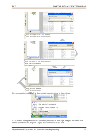
![RCE DIGITAL SIGNAL PROCESSING LAB
Department of Electronics & Communication Engineering 11
EXPERIMENT-2:
VERIFICATION OF LINEAR CONVOLUTION USING MATLAB AND CC STUDIO
AIM: To verify Linear Convolution using MATLAB AND CC STUDIO.
EQUIPMENT REQUIRED:
Hardware required Software Required
PC MATLAB
DSK6713 DSP Starter kit CCS Studio 3-1
USB Cable OS: Windows XP
Power Adapter
THEORY:
Convolution is a formal mathematical operation, just as multiplication, addition, and integration.
Addition takes two numbers and produces a third number, while convolution takes two signals and
produces a third signal. Convolution is used in the mathematics of many fields, such as probability
and statistics. In linear systems, convolution is used to describe the relationship between three signals
of interest: the input signal, the impulse response, and the output signal.
In this equation, x1(k), x2(n-k) and y(n) represent the input to and output from the system at time n.
Here we could see that one of the inputs is shifted in time by a value every time it is multiplied with
the other input signal. Linear Convolution is quite often used as a method of implementing filters of
various types.
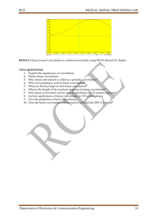
Linear Convolution Using MATLAB:-
Program:
clc;
clear all;
close all;
disp('linear convolution program');
x=input('enter i/p x(n):');
m=length(x);
h=input('enter i/p h(n):');
n=length(h);
x=[x,zeros(1,n)];
subplot(2,2,1), stem(x);
title('i/p sequence x(n)is:');
xlabel('---->n');
ylabel('---->x(n)');grid;
h=[h,zeros(1,m)];
subplot(2,2,2), stem(h);
title('i/p sequence h(n)is:');
xlabel('---->n');
ylabel('---->h(n)');grid;
disp('convolution of x(n) & h(n) is y(n):');
y=zeros(1,m+n-1);](https://image.slidesharecdn.com/dsplabmanual15-11-2016-190215035806/85/Dsp-lab-manual-15-11-2016-11-320.jpg)
![RCE DIGITAL SIGNAL PROCESSING LAB
Department of Electronics & Communication Engineering 12
for i=1:m+n-1
y(i)=0;
for j=1:m+n-1
if(j<i+1)
y(i)=y(i)+x(j)*h(i-j+1);
end
end
end
y
subplot(2,2,[3,4]),stem(y);
title('convolution of x(n) & h(n) is :');
xlabel('---->n');
ylabel('---->y(n)');grid;
Output :
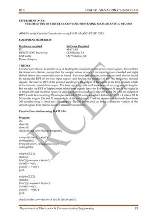
Linear Convolution Using CCSTUDIO:-
Procedure to create new Project:
1. To create project, go to Project and Select New.](https://image.slidesharecdn.com/dsplabmanual15-11-2016-190215035806/85/Dsp-lab-manual-15-11-2016-12-320.jpg)
![RCE DIGITAL SIGNAL PROCESSING LAB
Department of Electronics & Communication Engineering 14
Mathematical Formula:
The linear convolution of two continuous time signals x(t) and h(t) is defined by
For discrete time signals x(n) and h(n), is defined by
Where x(n) is the input signal and h(n) is the impulse response of the system.
In linear convolution length of output sequence is,
Length (y(n)) = length(x(n)) + length(h(n)) – 1
Program:
#include<stdio.h>
main()
{ int m=4; /*Lenght of i/p samples sequence*/
int n=4; /*Lenght of impulse response Co-efficients */
int i=0,j;
int x[10]={1,2,3,4,0,0,0,0}; /*Input Signal Samples*/
int h[10]={1,2,3,4,0,0,0,0}; /*Impulse Response Co-efficients*/
/*At the end of input sequences pad 'M' and 'N' no. of zero's*/
int *y;
y=(int *)0x0000100;
for(i=0;i<m+n-1;i++)
{
y[i]=0;
for(j=0;j<=i;j++)
y[i]+=x[j]*h[i-j];
}
for(i=0;i<m+n-1;i++)
printf("%dn",y[i]);
}
Output:
1, 4, 10, 20, 25, 24, 16.
4. Enter the source code and save the file with “.C” extension.](https://image.slidesharecdn.com/dsplabmanual15-11-2016-190215035806/85/Dsp-lab-manual-15-11-2016-14-320.jpg)
![RCE DIGITAL SIGNAL PROCESSING LAB
Department of Electronics & Communication Engineering 20
if(m-n~=0)
if(m>n)
h=[h,zeros(1,m-n)];
n=m;
end
x=[x,zeros(1,n-m)];
m=n;
end
y=zeros(1,n);
y(1)=0;
a(1)=h(1);
for j=2:n
a(j)=h(n-j+2);
end
%circular convolution
for i=1:n
y(1)=y(1)+x(i)*a(i);
end
for k=2:n
y(k)=0;
% circular shift
for j=2:n
x2(j)=a(j-1);
end
x2(1)=a(n);
for i=1:n
if(i<n+1)
a(i)=x2(i);
y(k)=y(k)+x(i)*a(i);
end
end
end
y
subplot(2,2,[3,4]),stem(y);
title('convolution of x(n) & h(n) is:');
xlabel('---->n');
ylabel('---->y(n)');grid;](https://image.slidesharecdn.com/dsplabmanual15-11-2016-190215035806/85/Dsp-lab-manual-15-11-2016-20-320.jpg)
![RCE DIGITAL SIGNAL PROCESSING LAB
Department of Electronics & Communication Engineering 22
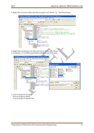
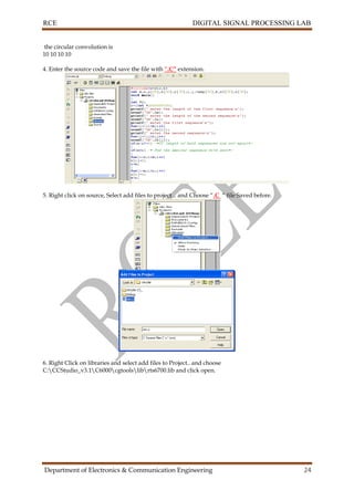
( Note: Location must be c:CCStudio_v3.1MyProjects ).
3. Click on File New Source File, to write the Source Code.
Circular Convolution:
Let x1(n) and x2(n) are finite duration sequences both of length N with DFT’s X1(k) and X2(k).
Convolution of two given sequences x1(n) and x2(n) is given by the equation,
x3(n) = IDFT[X3(k)]
X3(k) = X1(k) X2(k)
N-1
x3(n) = ∑ x1(m) x2((n-m))N
m=0
Program:
#include<stdio.h>
int m,n,x[30],h[30],y[30],i,j,temp[30],k,x2[30],a[30];
void main()
{
int *y;
y=(int *)0x0000100;
printf(" enter the length of the first sequencen");](https://image.slidesharecdn.com/dsplabmanual15-11-2016-190215035806/85/Dsp-lab-manual-15-11-2016-22-320.jpg)
![RCE DIGITAL SIGNAL PROCESSING LAB
Department of Electronics & Communication Engineering 23
scanf("%d",&m);
printf(" enter the length of the second sequencen");
scanf("%d",&n);
printf(" enter the first sequencen");
for(i=0;i<m;i++)
scanf("%d",&x[i]);
printf(" enter the second sequencen");
for(j=0;j<n;j++)
scanf("%d",&h[j]);
if(m-n!=0) /*If length of both sequences are not equal*/
{
if(m>n) /* Pad the smaller sequence with zero*/
{
for(i=n;i<m;i++)
h[i]=0;
n=m;
}
for(i=m;i<n;i++)
x[i]=0;
m=n;
}
y[0]=0;
a[0]=h[0];
for(j=1;j<n;j++) /*folding h(n) to h(-n)*/
a[j]=h[n-j];
/*Circular convolution*/
for(i=0;i<n;i++)
y[0]+=x[i]*a[i];
for(k=1;k<n;k++)
{
y[k]=0;
/*circular shift*/
for(j=1;j<n;j++)
x2[j]=a[j-1];
x2[0]=a[n-1];
for(i=0;i<n;i++)
{
a[i]=x2[i];
y[k]+=x[i]*x2[i];
}}
/*displaying the result*/
printf(" the circular convolution isn");
for(i=0;i<n;i++)
printf("%d ",y[i]);
}
Output:
enter the length of the first sequence
4
enter the length of the second sequence
4
enter the first sequence
4 3 2 1
enter the second sequence
1 1 1 1](https://image.slidesharecdn.com/dsplabmanual15-11-2016-190215035806/85/Dsp-lab-manual-15-11-2016-23-320.jpg)
![RCE DIGITAL SIGNAL PROCESSING LAB
Department of Electronics & Communication Engineering 31
disp('Rectangular window filter response');
end
if (c==2)
y=triang(n1);
disp('Triangular window filter response');
end
if(c==3)
y=kaiser(n1);
disp('kaiser window filter response');
end
%LPF
b=fir1(n,wp,y);
[h,o]=freqz(b,1,256);
m=20*log10(abs(h));
subplot(2,2,1);plot(o/pi,m);
title('LPF');
ylabel('Gain in dB-->');
xlabel('(a) Normalized frequency-->');
%HPF
b=fir1(n,wp,'high',y);
[h,o]=freqz(b,1,256);
m=20*log10(abs(h));
subplot(2,2,2);plot(o/pi,m);
title('HPF');
ylabel('Gain in dB-->');
xlabel('(b) Normalized frequency-->');
%BPF
wn=[wp ws];
b=fir1(n,wn,y);
[h,o]=freqz(b,1,256);
m=20*log10(abs(h));
subplot(2,2,3);plot(o/pi,m);
title('BPF');
ylabel('Gain in dB-->');
xlabel('(c) Normalized frequency-->');
%BSF
b=fir1(n,wn,'stop',y);
[h,o]=freqz(b,1,256);
m=20*log10(abs(h));
subplot(2,2,4);plot(o/pi,m);
title('BSF');
ylabel('Gain in dB-->');
xlabel('(d) Normalized frequency-->');](https://image.slidesharecdn.com/dsplabmanual15-11-2016-190215035806/85/Dsp-lab-manual-15-11-2016-31-320.jpg)
![RCE DIGITAL SIGNAL PROCESSING LAB
Department of Electronics & Communication Engineering 33
C PROGRAM FOR KAISER WINDOW LPF:
#include "filtercfg.h"
#include "dsk6713.h"
#include "dsk6713_aic23.h"
#include "stdio.h"
//float filter_coeff[]={-0.000019,-0.000170,-0.000609,-0.001451,-0.002593,
// -0.003511,-0.003150,0.000000,0.007551,0.020655,
// 0.039383,0.062306,0.086494,0.108031,0.122944,
// 0.128279,0.122944,0.108031,0.086494,0.062306,
// 0.039383,0.020655,0.007551,0.000000,-0.003150,
// -0.003511,-0.002593,-0.001451,-0.000609,-0.000710,
// -0.000019};// kaiser low pass fir filter pass band range 0-
500Hz
//float filter_coeff[]={-0.000035,-0.000234,-0.000454,0.000000,0.001933,
// 0.004838,0.005671,-0.000000,-0.013596,-0.028462,
// -0.029370,0.000000,0.064504,0.148863,0.221349,
// 0.249983,0.221349,0.148863,0.064504,0.000000,
// -0.029370,-0.028462,-0.013596,-0.000000,0.005671,
// 0.004838,0.001933,0.000000,-0.000454,-0.000234,
// -0.000035};// kaiser low pass fir filter pass band range 0-1000Hz
float filter_coeff[]={-0.000046,-0.000166,0.000246,0.001414,0.001046,
-0.003421,-0.007410,0.000000,0.017764,0.020126,
-0.015895,-0.060710,-0.034909,0.105263,0.289209,
0.374978,0.289209,0.105263,-0.034909,-0.060710,
-0.015895,0.020126,0.017764,0.000000,-0.007410,](https://image.slidesharecdn.com/dsplabmanual15-11-2016-190215035806/85/Dsp-lab-manual-15-11-2016-33-320.jpg)
![RCE DIGITAL SIGNAL PROCESSING LAB
Department of Electronics & Communication Engineering 34
-0.003421,0.001046,0.001414,0.000246,-0.000166,
-0.000046};//Kaiser low pass fir filter pass band range 0-1500Hz
//static short int in_buffer[100];
DSK6713_AIC23_Config
config={0x0017,0x0017,0x00d8,0x00d8,0x0011,0x0000,0x0000,0x0043,0x0081,0x0001};
void main()
{
DSK6713_AIC23_CodecHandle hCodec;
Uint32 l_input, r_input,l_output, r_output;
DSK6713_init();
hCodec = DSK6713_AIC23_openCodec(0, &config);
DSK6713_AIC23_setFreq(hCodec, 1);
while(1)
{
while(!DSK6713_AIC23_read(hCodec, &l_input));
while(!DSK6713_AIC23_read(hCodec, &r_input));
l_output=(Int16)FIR_FILTER(&filter_coeff ,l_input);
r_output=l_output;
while(!DSK6713_AIC23_write(hCodec, l_output));
while(!DSK6713_AIC23_write(hCodec, r_output));
}
DSK6713_AIC23_closeCodec(hCodec);
}
signed int FIR_FILTER(float * h, signed int x)
{
int i=0;
signed long output=0;
static short int in_buffer[100];
in_buffer[0] = x;
for(i=30;i>0;i--)
in_buffer[i] = in_buffer[i-1];
for(i=0;i<32;i++)
output = output + h[i] * in_buffer[i];
//output = x;
return(output);
}
KAISER WINDOW HPF:
#include "filtercfg.h"
#include "dsk6713.h"](https://image.slidesharecdn.com/dsplabmanual15-11-2016-190215035806/85/Dsp-lab-manual-15-11-2016-34-320.jpg)
![RCE DIGITAL SIGNAL PROCESSING LAB
Department of Electronics & Communication Engineering 35
#include "dsk6713_aic23.h"
#include "stdio.h"
//float filter_coeff[]={0.000050,0.000223,0.000520,0.000831,0.000845,
// -0.000000,-0.002478,-0.007437,-0.015556,-0.027071,
// -0.041538,-0.057742,-0.073805,-0.087505,-0.096739,
// 0.899998,-0.096739,-0.087505,-0.073805,-0.057742,
// -0.041538,-0.027071,-0.015556,-0.007437,-0.002478,
// -0.000000,0.000845,0.000831,0.000520,0.000223,
// 0.000050};//FIR High pass Kaiser filter pass band range 400Hz-3.5KHz
float filter_coeff[]={0.000000,-0.000138,-0.000611,-0.001345,-0.001607,
-0.000000,0.004714,0.012033,0.018287,0.016731,
0.000000,-0.035687,-0.086763,-0.141588,-0.184011,
0.800005,-0.184011,-0.141588,-0.086763,-0.035687,
0.000000,0.016731,0.018287,0.012033,0.004714,
-0.000000,-0.001607,-0.001345,-0.000611,-0.000138,
0.000000};//FIR High pass Kaiser filter pass band range
800Hz-3.5KHz
//float filter_coeff[]={-0.000050,-0.000138,0.000198,0.001345,0.002212,-0.000000,
// -0.006489,-0.012033,-0.005942,0.016731,0.041539,0.035687,
// -0.028191,-0.141589,-0.253270,0.700008,-0.253270,-0.141589,
// -0.028191,0.035687,0.041539,0.016731,-0.005942,-0.012033,
// -0.006489,-0.000000,0.002212,0.001345,0.000198,-0.000138,
// -0.000050};//FIR High pass Kaiser filter pass band range
1200Hz-3.5KHz
//static short int in_buffer[100];
DSK6713_AIC23_Config
config={0x0017,0x0017,0x00d8,0x00d8,0x0011,0x0000,0x0000,0x0043,0x0081,0x0001};
void main()
{
DSK6713_AIC23_CodecHandle hCodec;
Uint32 l_input, r_input,l_output, r_output;
DSK6713_init();
hCodec = DSK6713_AIC23_openCodec(0, &config);
DSK6713_AIC23_setFreq(hCodec, 1);
while(1)
{
while(!DSK6713_AIC23_read(hCodec, &l_input));
while(!DSK6713_AIC23_read(hCodec, &r_input));
l_output=(Int16)FIR_FILTER(&filter_coeff ,l_input);
r_output=l_output;
while(!DSK6713_AIC23_write(hCodec, l_output));
while(!DSK6713_AIC23_write(hCodec, r_output));](https://image.slidesharecdn.com/dsplabmanual15-11-2016-190215035806/85/Dsp-lab-manual-15-11-2016-35-320.jpg)
![RCE DIGITAL SIGNAL PROCESSING LAB
Department of Electronics & Communication Engineering 36
}
DSK6713_AIC23_closeCodec(hCodec);
}
signed int FIR_FILTER(float * h, signed int x)
{
int i=0;
signed long output=0;
static short int in_buffer[100];
in_buffer[0] = x;
for(i=30;i>0;i--)
in_buffer[i] = in_buffer[i-1];
for(i=0;i<32;i++)
output = output + h[i] * in_buffer[i];
//output = x;
return(output);
}
RECTANGULAR LPF:
#include "filtercfg.h"
#include "dsk6713.h"
#include "dsk6713_aic23.h"
#include "stdio.h"
//float filter_coeff[]={-0.008982,-0.017782,-0.025020,-0.029339,-0.029569,
// -0.024895,-0.014970,0.000000,0.019247,0.041491,
// 0.065053,0.088016,0.108421,0.124473,0.134729,
// 0.138255,0.134729,0.124473,0.108421,0.088016,
// 0.065053,0.041491,0.019247,0.000000,-0.014970,
// -0.024895,-0.029569,-0.029339,-0.025020,-0.017782,
// -0.008982};//FIR Low pass Rectangular Filter pass band
range 0-500Hz
//float filter_coeff[]={-0.015752,-0.023869,-0.018176,0.000000,0.021481,
// 0.033416,0.026254,-0.000000,-0.033755,-0.055693,
// -0.047257,0.000000,0.078762,0.167080,0.236286,
// 0.262448,0.236286,0.167080,0.078762,0.000000,
// -0.047257,-0.055693,-0.033755,-0.000000,0.026254,
// 0.033416,0.021481,0.000000,-0.018176,-0.023869,
// -0.015752};//FIR Low pass Rectangular Filter pass band
range 0-1000Hz
float filter_coeff[]={-0.020203,-0.016567,0.009656,0.027335,0.011411,
-0.023194,-0.033672,0.000000,0.043293,0.038657,
-0.025105,-0.082004,-0.041842,0.115971,0.303048,
0.386435,0.303048,0.115971,-0.041842,-0.082004,
-0.025105,0.038657,0.043293,0.000000,-0.033672,
-0.023194,0.011411,0.027335,0.009656,-0.016567,
-0.020203};//FIR Low pass Rectangular Filter pass band range 0-1500Hz
//static short int in_buffer[100];](https://image.slidesharecdn.com/dsplabmanual15-11-2016-190215035806/85/Dsp-lab-manual-15-11-2016-36-320.jpg)
![RCE DIGITAL SIGNAL PROCESSING LAB
Department of Electronics & Communication Engineering 37
DSK6713_AIC23_Config
config={0x0017,0x0017,0x00d8,0x00d8,0x0011,0x0000,0x0000,0x0043,0x0081,0x0001};
void main()
{
DSK6713_AIC23_CodecHandle hCodec;
Uint32 l_input, r_input,l_output, r_output;
DSK6713_init();
hCodec = DSK6713_AIC23_openCodec(0, &config);
DSK6713_AIC23_setFreq(hCodec, 1);
while(1)
{
while(!DSK6713_AIC23_read(hCodec, &l_input));
while(!DSK6713_AIC23_read(hCodec, &r_input));
l_output=(Int16)FIR_FILTER(&filter_coeff ,l_input);
r_output=l_output;
while(!DSK6713_AIC23_write(hCodec, l_output));
while(!DSK6713_AIC23_write(hCodec, r_output));
}
DSK6713_AIC23_closeCodec(hCodec);
}
signed int FIR_FILTER(float * h, signed int x)
{
int i=0;
signed long output=0;
static short int in_buffer[100];
in_buffer[0] = x;
for(i=30;i>0;i--)
in_buffer[i] = in_buffer[i-1];
for(i=0;i<32;i++)
output = output + h[i] * in_buffer[i];
//output = x;
return(output);
}
RECTANGULAR HPF:
#include "filtercfg.h"
#include "dsk6713.h"
#include "dsk6713_aic23.h"
#include "stdio.h"
//float filter_coeff[]={0.021665,0.022076,0.020224,0.015918,0.009129,
// -0.000000,-0.011158,-0.023877,-0.037558,-0.051511,](https://image.slidesharecdn.com/dsplabmanual15-11-2016-190215035806/85/Dsp-lab-manual-15-11-2016-37-320.jpg)
![RCE DIGITAL SIGNAL PROCESSING LAB
Department of Electronics & Communication Engineering 38
// -0.064994,-0.077266,-0.087636,-0.095507,-0.100422,
// 0.918834,-0.100422,-0.095507,-0.087636,-0.077266,
// -0.064994,-0.051511,-0.037558,-0.023877,-0.011158,
// -0.000000,0.009129,0.015918,0.020224,0.022076,
// 0.021665};//FIR High pass Rectangular filter pass band range 400Hz-3.5KHz
float filter_coeff[]={0.000000,-0.013457,-0.023448,-0.025402,-0.017127,
-0.000000,0.020933,0.038103,0.043547,0.031399,
0.000000,-0.047098,-0.101609,-0.152414,-0.188394,
0.805541,-0.188394,-0.152414,-0.101609,-0.047098,
0.000000,0.031399,0.043547,0.038103,0.020933,
-0.000000,-0.017127,-0.025402,-0.023448,-0.013457,
0.000000};//FIR High pass Rectangular filter pass band
range 800Hz-3.5KHz
//float filter_coeff[]={-0.020798,-0.013098,0.007416,0.024725,0.022944,
// -0.000000,-0.028043,-0.037087,-0.013772,0.030562,
// 0.062393,0.045842,-0.032134,-0.148349,-0.252386,
// 0.686050,-0.252386,-0.148349,-0.032134,0.045842,
// 0.062393,0.030562,-0.013772,-0.037087,-0.028043,
// -0.000000,0.022944,0.024725,0.007416,-0.013098,
// -0.020798};//FIR High pass Rectangular filter pass band range 1200Hz-3.5KHz
//static short int in_buffer[100];
DSK6713_AIC23_Config
config={0x0017,0x0017,0x00d8,0x00d8,0x0011,0x0000,0x0000,0x0043,0x0081,0x0001};
void main()
{
DSK6713_AIC23_CodecHandle hCodec;
Uint32 l_input, r_input,l_output, r_output;
DSK6713_init();
hCodec = DSK6713_AIC23_openCodec(0, &config);
DSK6713_AIC23_setFreq(hCodec, 1);
while(1)
{
while(!DSK6713_AIC23_read(hCodec, &l_input));
while(!DSK6713_AIC23_read(hCodec, &r_input));
l_output=(Int16)FIR_FILTER(&filter_coeff ,l_input);
r_output=l_output;
while(!DSK6713_AIC23_write(hCodec, l_output));
while(!DSK6713_AIC23_write(hCodec, r_output));
}
DSK6713_AIC23_closeCodec(hCodec);](https://image.slidesharecdn.com/dsplabmanual15-11-2016-190215035806/85/Dsp-lab-manual-15-11-2016-38-320.jpg)
![RCE DIGITAL SIGNAL PROCESSING LAB
Department of Electronics & Communication Engineering 39
}
signed int FIR_FILTER(float * h, signed int x)
{
int i=0;
signed long output=0;
static short int in_buffer[100];
in_buffer[0] = x;
for(i=30;i>0;i--)
in_buffer[i] = in_buffer[i-1];
for(i=0;i<32;i++)
output = output + h[i] * in_buffer[i];
//output = x;
return(output);
}
TRANGULAR LPF:
#include "filtercfg.h"
#include "dsk6713.h"
#include "dsk6713_aic23.h"
#include "stdio.h"
//float filter_coeff[]={0.000000,-0.001185,-0.003336,-0.005868,-0.007885,
// -0.008298,-0.005988,0.000000,0.010265,0.024895,
// 0.043368,0.064545,0.086737,0.107877,0.125747,
// 0.138255,0.125747,0.107877,0.086737,0.064545,
// 0.043368,0.024895,0.010265,0.000000,-0.005988,
// -0.008298,-0.007885,-0.005868,-0.003336,-0.001185,
// 0.000000};//FIR Low pass Triangular Filter pass band range 0-500Hz
//float filter_coeff[]={0.000000,-0.001591,-0.002423,0.000000,0.005728,
// 0.011139,0.010502,-0.000000,-0.018003,-0.033416,
// -0.031505,0.000000,0.063010,0.144802,0.220534,
// 0.262448,0.220534,0.144802,0.063010,0.000000,
// -0.031505,-0.033416,-0.018003,-0.000000,0.010502,
// 0.011139,0.005728,0.000000,-0.002423,-0.001591,
// 0.000000};//FIR Low pass Triangular Filter pass band range 0-1000Hz
float filter_coeff[]={0.000000,-0.001104,0.001287,0.005467,0.003043,
-0.007731,-0.013469,0.000000,0.023089,0.023194,
-0.016737,-0.060136,-0.033474,0.100508,0.282844,
0.386435,0.282844,0.100508,-0.033474,-0.060136,
-0.016737,0.023194,0.023089,0.000000,-0.013469,
-0.007731,0.003043,0.005467,0.001287,-0.001104,
0.000000};//FIR Low pass Triangular Filter pass band range 0-1500Hz
//static short int in_buffer[100];
DSK6713_AIC23_Config
config={0x0017,0x0017,0x00d8,0x00d8,0x0011,0x0000,0x0000,0x0043,0x0081,0x0001};](https://image.slidesharecdn.com/dsplabmanual15-11-2016-190215035806/85/Dsp-lab-manual-15-11-2016-39-320.jpg)
![RCE DIGITAL SIGNAL PROCESSING LAB
Department of Electronics & Communication Engineering 40
void main()
{
DSK6713_AIC23_CodecHandle hCodec;
Uint32 l_input, r_input,l_output, r_output;
DSK6713_init();
hCodec = DSK6713_AIC23_openCodec(0, &config);
DSK6713_AIC23_setFreq(hCodec, 1);
while(1)
{
while(!DSK6713_AIC23_read(hCodec, &l_input));
while(!DSK6713_AIC23_read(hCodec, &r_input));
l_output=(Int16)FIR_FILTER(&filter_coeff ,l_input);
r_output=l_output;
while(!DSK6713_AIC23_write(hCodec, l_output));
while(!DSK6713_AIC23_write(hCodec, r_output));
}
DSK6713_AIC23_closeCodec(hCodec);
}
signed int FIR_FILTER(float * h, signed int x)
{
int i=0;
signed long output=0;
static short int in_buffer[100];
in_buffer[0] = x;
for(i=30;i>0;i--)
in_buffer[i] = in_buffer[i-1];
for(i=0;i<32;i++)
output = output + h[i] * in_buffer[i];
//output = x;
return(output);
}
TRANGULAR HPF
#include "filtercfg.h"
#include "dsk6713.h"
#include "dsk6713_aic23.h"
#include "stdio.h"
//float filter_coeff[]={0.000000,0.001445,0.002648,0.003127,0.002391,
// -0.000000,-0.004383,-0.010943,-0.019672,-0.030353,
// -0.042554,-0.055647,-0.068853,-0.081290,-0.092048,
// 0.902380,-0.092048,-0.081290,-0.068853,-0.055647,
// -0.042554,-0.030353,-0.019672,-0.010943,-0.004383,](https://image.slidesharecdn.com/dsplabmanual15-11-2016-190215035806/85/Dsp-lab-manual-15-11-2016-40-320.jpg)
![RCE DIGITAL SIGNAL PROCESSING LAB
Department of Electronics & Communication Engineering 41
// -0.000000,0.002391,0.003127,0.002648,0.001445,
// 0.000000};//FIR High pass Triangular filter pass band range
400Hz-3.5KHz
//float filter_coeff[]={0.000000,-0.000897,-0.003126,-0.005080,-0.004567,
// -0.000000,0.008373,0.017782,0.023225,0.018839,
// 0.000000,-0.034539,-0.081287,-0.132092,-0.175834,
// 0.805541,-0.175834,-0.132092,-0.081287,-0.034539,
// 0.000000,0.018839,0.023225,0.017782,0.008373,
// -0.000000,-0.004567,-0.005080,-0.003126,-0.000897,
// 0.000000};//FIR High pass Triangular filter pass band range
800Hz-3.5KHz
float filter_coeff[]={0.000000,-0.000901,0.001021,0.005105,0.006317,
-0.000000,-0.011581,-0.017868,-0.007583,0.018931,
0.042944,0.034707,-0.026541,-0.132736,-0.243196,
0.708287,-0.243196,-0.132736,-0.026541,0.034707,
0.042944,0.018931,-0.007583,-0.017868,-0.011581,
-0.000000,0.006317,0.005105,0.001021,-0.000901,
0.000000};//FIR High pass Triangular filter pass band range
1200Hz-3.5KHz
//static short int in_buffer[100];
DSK6713_AIC23_Config
config={0x0017,0x0017,0x00d8,0x00d8,0x0011,0x0000,0x0000,0x0043,0x0081,0x0001};
void main()
{
DSK6713_AIC23_CodecHandle hCodec;
Uint32 l_input, r_input,l_output, r_output;
DSK6713_init();
hCodec = DSK6713_AIC23_openCodec(0, &config);
DSK6713_AIC23_setFreq(hCodec, 1);
while(1)
{
while(!DSK6713_AIC23_read(hCodec, &l_input));
while(!DSK6713_AIC23_read(hCodec, &r_input));
l_output=(Int16)FIR_FILTER(&filter_coeff ,l_input);
r_output=l_output;
while(!DSK6713_AIC23_write(hCodec, l_output));
while(!DSK6713_AIC23_write(hCodec, r_output));
}
DSK6713_AIC23_closeCodec(hCodec);
}](https://image.slidesharecdn.com/dsplabmanual15-11-2016-190215035806/85/Dsp-lab-manual-15-11-2016-41-320.jpg)
![RCE DIGITAL SIGNAL PROCESSING LAB
Department of Electronics & Communication Engineering 42
signed int FIR_FILTER(float * h, signed int x)
{
int i=0;
signed long output=0;
static short int in_buffer[100];
in_buffer[0] = x;
for(i=30;i>0;i--)
in_buffer[i] = in_buffer[i-1];
for(i=0;i<32;i++)
output = output + h[i] * in_buffer[i];
//output = x;
return(output);
}
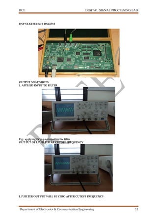
DSP STARTER KIT DSK6713
SNAP SHOTS:
1. APPLIED INPUT TO FILTER
Fig : applying 2V p-p as input for the filter](https://image.slidesharecdn.com/dsplabmanual15-11-2016-190215035806/85/Dsp-lab-manual-15-11-2016-42-320.jpg)
![RCE DIGITAL SIGNAL PROCESSING LAB
Department of Electronics & Communication Engineering 45
EXPERIMENT NO-5:
IIR FILTER (LP/HP) IMPLEMENTATION ON DSP PROCESSORS
AIM: To implement the IIR FILTERS (LPF/HPF) on DSK 6713 DSP starter kit
EQUIPMENT REQUIRED:
Hardware required Software Required
PC MATLAB
DSK6713 DSP Starter kit CCS Studio 3-1
USB Cable OS: Windows XP
Power Adapter
CRO, Probes, Function Generator
THEORY:
The IIR filter can realize both the poles and zeroes of a system because it has a rational transfer
function, described by polynomials in z in both the numerator and the denominator
m and n are order of the two polynomials b and a are the filter coefficients. These
filter coefficients are generated using FDS (Filter Design software or Digital Filter design package. IIR
filters can be expanded as infinite impulse response filters. In designing IIR filters, cutoff frequencies
of the filters should be mentioned. The order of the filter can be estimated using Butterworth
polynomial. That’s why the filters are named as Butterworth filters. Filter coefficients can be found
and the response can be plotted.
C PROGRAM IIR_BUTERWORTH_LP FILTER
#include "filtercfg.h"
#include "dsk6713.h"
#include "dsk6713_aic23.h"
#include "stdio.h"
//const signed int filter_coeff[] = {2366,2366,2366,32767,-18179,13046};//IIR_BUTTERWORTH_LP
FILTER pass band range 0-2.5kHZ
//const signed int filter_coeff[] = {312,312,312,32767,-27943,24367};//IIR_BUTTERWORTH_LP
FILTER pass band range 0-800Hz
const signed int filter_coeff[] = {15241,15241,15241,32761,10161,7877};//IIR_BUTERWORTH_LP
FILTER pass band range 0-8kHz
DSK6713_AIC23_Config
config={0x0017,0x0017,0x00d8,0x00d8,0x0011,0x0000,0x0000,0x0043,0x0081,0x0001};
void main()
{
DSK6713_AIC23_CodecHandle hCodec;
Uint32 l_input, r_input,l_output, r_output;
DSK6713_init();
hCodec = DSK6713_AIC23_openCodec(0, &config);
DSK6713_AIC23_setFreq(hCodec, 3);](https://image.slidesharecdn.com/dsplabmanual15-11-2016-190215035806/85/Dsp-lab-manual-15-11-2016-45-320.jpg)
![RCE DIGITAL SIGNAL PROCESSING LAB
Department of Electronics & Communication Engineering 46
while(1)
{
while(!DSK6713_AIC23_read(hCodec, &l_input));
while(!DSK6713_AIC23_read(hCodec, &r_input));
l_output=IIR_FILTER(&filter_coeff ,l_input);
r_output=l_output;
while(!DSK6713_AIC23_write(hCodec, l_output));
while(!DSK6713_AIC23_write(hCodec, r_output));
}
DSK6713_AIC23_closeCodec(hCodec);
}
signed int IIR_FILTER(const signed int * h, signed int x1)
{
static signed int x[6] = {0,0,0,0,0,0};
static signed int y[6] = {0,0,0,0,0,0};
int temp=0;
temp = (short int)x1;
x[0] = (signed int) temp;
temp = ( (int)h[0] * x[0]);
temp += ( (int)h[1] * x[1]);
temp += ( (int)h[1] * x[1]);
temp += ( (int)h[2] * x[2]);
temp -= ( (int)h[4] * y[1]);
temp -= ( (int)h[4] * y[1]);
temp -= ( (int)h[5] * y[2]);
temp >>=15;
if ( temp > 32767 )
{
temp = 32767;
}
else if ( temp < -32767)
{
temp = -32767;
}
y[0] = temp;
y[2] = y[1];
y[1] = y[0];
x[2] = x[1];
x[1] = x[0];](https://image.slidesharecdn.com/dsplabmanual15-11-2016-190215035806/85/Dsp-lab-manual-15-11-2016-46-320.jpg)
![RCE DIGITAL SIGNAL PROCESSING LAB
Department of Electronics & Communication Engineering 47
return (temp<<2);
}
IIR BUTTERWORTH HP FILTER
#include "filtercfg.h"
#include "dsk6713.h"
#include "dsk6713_aic23.h"
#include "stdio.h"
//const signed int filter_coeff[] = {20539,-20539,20539,32767,-
18173,13406};//IIR_BUTTERWORTH_HP FILTER pass band range 2.5kHz-11KHz
//const signed int filter_coeff[] = {15241,-15241,15241,32761,-10161,7877};//IIR_BUTTERWORTH_HP
FILTER pass band range 4kHz-11KHz
const signed int filter_coeff[] = { 7215,-7215,7215,32767,5039,6171};//IIR_BUTTERWORTH_HP
FILTER pass band range 7kHz-11Khz
DSK6713_AIC23_Config
config={0x0017,0x0017,0x00d8,0x00d8,0x0011,0x0000,0x0000,0x0043,0x0081,0x0001};
void main()
{
DSK6713_AIC23_CodecHandle hCodec;
Uint32 l_input, r_input,l_output, r_output;
DSK6713_init();
hCodec = DSK6713_AIC23_openCodec(0, &config);
DSK6713_AIC23_setFreq(hCodec, 3);
while(1)
{
while(!DSK6713_AIC23_read(hCodec, &l_input));
while(!DSK6713_AIC23_read(hCodec, &r_input));
l_output=IIR_FILTER(&filter_coeff ,l_input);
r_output=l_output;
while(!DSK6713_AIC23_write(hCodec, l_output));
while(!DSK6713_AIC23_write(hCodec, r_output));
}
DSK6713_AIC23_closeCodec(hCodec);
}
signed int IIR_FILTER(const signed int * h, signed int x1)
{
static signed int x[6] = {0,0,0,0,0,0};
static signed int y[6] = {0,0,0,0,0,0};](https://image.slidesharecdn.com/dsplabmanual15-11-2016-190215035806/85/Dsp-lab-manual-15-11-2016-47-320.jpg)
![RCE DIGITAL SIGNAL PROCESSING LAB
Department of Electronics & Communication Engineering 48
int temp=0;
temp = (short int)x1;
x[0] = (signed int) temp;
temp = ( (int)h[0] * x[0]);
temp += ( (int)h[1] * x[1]);
temp += ( (int)h[1] * x[1]);
temp += ( (int)h[2] * x[2]);
temp -= ( (int)h[4] * y[1]);
temp -= ( (int)h[4] * y[1]);
temp -= ( (int)h[5] * y[2]);
temp >>=15;
if ( temp > 32767 )
{
temp = 32767;
}
else if ( temp < -32767)
{
temp = -32767;
}
y[0] = temp;
y[2] = y[1];
y[1] = y[0];
x[2] = x[1];
x[1] = x[0];
return (temp<<2);
}
IIR CHEBYSHEV LP FILTER
#include "filtercfg.h"
#include "dsk6713.h"
#include "dsk6713_aic23.h"
#include "stdio.h"
//const signed int filter_coeff[] = {1455,1455,1455,32767,-23410,21735};//IIR_CHEB_LP FILTER pass
band range 0-2.5kHz
//const signed int filter_coeff[] = {168,168,168,32767,-30225,28637};//IIR_CHEB_LP FILTER pass
band range 0-800Hz
const signed int filter_coeff[] = {11617,11617,11617,32767,8683,15506};//IIR_CHEB_LP FILTER pass
band range 0-8kHz
DSK6713_AIC23_Config
config={0x0017,0x0017,0x00d8,0x00d8,0x0011,0x0000,0x0000,0x0043,0x0081,0x0001};](https://image.slidesharecdn.com/dsplabmanual15-11-2016-190215035806/85/Dsp-lab-manual-15-11-2016-48-320.jpg)
![RCE DIGITAL SIGNAL PROCESSING LAB
Department of Electronics & Communication Engineering 49
void main()
{
DSK6713_AIC23_CodecHandle hCodec;
Uint32 l_input, r_input,l_output, r_output;
DSK6713_init();
hCodec = DSK6713_AIC23_openCodec(0, &config);
DSK6713_AIC23_setFreq(hCodec, 3);
while(1)
{
while(!DSK6713_AIC23_read(hCodec, &l_input));
while(!DSK6713_AIC23_read(hCodec, &r_input));
l_output=IIR_FILTER(&filter_coeff ,l_input);
r_output=l_output;
while(!DSK6713_AIC23_write(hCodec, l_output));
while(!DSK6713_AIC23_write(hCodec, r_output));
}
DSK6713_AIC23_closeCodec(hCodec);
}
signed int IIR_FILTER(const signed int * h, signed int x1)
{
static signed int x[6] = {0,0,0,0,0,0};
static signed int y[6] = {0,0,0,0,0,0};
int temp=0;
temp = (short int)x1;
x[0] = (signed int) temp;
temp = ( (int)h[0] * x[0]);
temp += ( (int)h[1] * x[1]);
temp += ( (int)h[1] * x[1]);
temp += ( (int)h[2] * x[2]);
temp -= ( (int)h[4] * y[1]);
temp -= ( (int)h[4] * y[1]);
temp -= ( (int)h[5] * y[2]);
temp >>=15;
if ( temp > 32767 )
{
temp = 32767;
}
else if ( temp < -32767)](https://image.slidesharecdn.com/dsplabmanual15-11-2016-190215035806/85/Dsp-lab-manual-15-11-2016-49-320.jpg)
![RCE DIGITAL SIGNAL PROCESSING LAB
Department of Electronics & Communication Engineering 50
{
temp = -32767;
}
y[0] = temp;
y[2] = y[1];
y[1] = y[0];
x[2] = x[1];
x[1] = x[0];
return (temp<<2);
}
IIR CHEBYSHEV HP FILTER
#include "filtercfg.h"
#include "dsk6713.h"
#include "dsk6713_aic23.h"
#include "stdio.h"
//const signed int filter_coeff[] = {12730,-12730,12730,32767,-18324,21137};//IIR_CHEB_HP FILTER
pass band range 2.5kHz-11KHz
//const signed int filter_coeff[] = {9268,-9268,9268,32767,-7395,18367};//IIR_CHEB_HP FILTER pass
band range 4kHz-11KHz
const signed int filter_coeff[] = { 3842,-3842,3842,32767,12360,19289};//IIR_CHEB_HP FILTER pass
band range 7kz-11KHz
DSK6713_AIC23_Config
config={0x0017,0x0017,0x00d8,0x00d8,0x0011,0x0000,0x0000,0x0043,0x0081,0x0001};
void main()
{
DSK6713_AIC23_CodecHandle hCodec;
Uint32 l_input, r_input,l_output, r_output;
DSK6713_init();
hCodec = DSK6713_AIC23_openCodec(0, &config);
DSK6713_AIC23_setFreq(hCodec, 3);
while(1)
{
while(!DSK6713_AIC23_read(hCodec, &l_input));
while(!DSK6713_AIC23_read(hCodec, &r_input));
l_output=IIR_FILTER(&filter_coeff ,l_input);
r_output=l_output;
while(!DSK6713_AIC23_write(hCodec, l_output));
while(!DSK6713_AIC23_write(hCodec, r_output));
}
DSK6713_AIC23_closeCodec(hCodec);
}](https://image.slidesharecdn.com/dsplabmanual15-11-2016-190215035806/85/Dsp-lab-manual-15-11-2016-50-320.jpg)
![RCE DIGITAL SIGNAL PROCESSING LAB
Department of Electronics & Communication Engineering 51
signed int IIR_FILTER(const signed int * h, signed int x1)
{
static signed int x[6] = {0,0,0,0,0,0};
static signed int y[6] = {0,0,0,0,0,0};
int temp=0;
temp = (short int)x1;
x[0] = (signed int) temp;
temp = ( (int)h[0] * x[0]);
temp += ( (int)h[1] * x[1]);
temp += ( (int)h[1] * x[1]);
temp += ( (int)h[2] * x[2]);
temp -= ( (int)h[4] * y[1]);
temp -= ( (int)h[4] * y[1]);
temp -= ( (int)h[5] * y[2]);
temp >>=15;
if ( temp > 32767 )
{
temp = 32767;
}
else if ( temp < -32767)
{
temp = -32767;
}
y[0] = temp;
y[2] = y[1];
y[1] = y[0];
x[2] = x[1];
x[1] = x[0];
return (temp<<2);
}](https://image.slidesharecdn.com/dsplabmanual15-11-2016-190215035806/85/Dsp-lab-manual-15-11-2016-51-320.jpg)
![RCE DIGITAL SIGNAL PROCESSING LAB
Department of Electronics & Communication Engineering 59
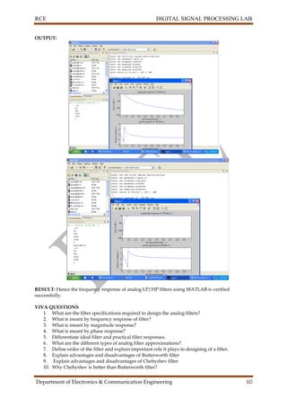
EXPERIMENT NO-8:
VERIFICATION THE FREQUENCY RESPONSE OF ANALOG LP/HP FILTERS USING MATLAB
AIM: To verify the frequency response of analog LP/HP filters using MATLAB.
EQUIPMENT REQUIRED:
Hardware required Software Required
PC MATLAB
OS: Windows XP
THEORY:
Analog Low pass filter & High pass filter are obtained by using Butterworth or Chebyshev filter with
coefficients are given. The frequency – magnitude plot gives the frequency response of the filter.
PROGRAM:
clc;
clear all;
close all;
warning off;
disp('enter the IIR filter design specifications');
rp=input('enter the passband ripple');
rs=input('enter the stopband ripple');
wp=input('enter the passband freq');
ws=input('enter the stopband freq');
fs=input('enter the sampling freq');
w1=2*wp/fs;w2=2*ws/fs;
[n,wn]=buttord(w1,w2,rp,rs,'s');
c=input('enter choice of filter 1. LPF 2. HPF n ');
if(c==1)
disp('Frequency response of IIR LPF is:');
[b,a]=butter(n,wn,'low','s');
end
if(c==2)
disp('Frequency response of IIR HPF is:');
[b,a]=butter(n,wn,'high','s');
end
w=0:.01:pi;
[h,om]=freqs(b,a,w);
m=20*log10(abs(h));
an=angle(h);
figure,subplot(2,1,1);plot(om/pi,m);
title('magnitude response of IIR filter is:');
xlabel('(a) Normalized freq. -->');
ylabel('Gain in dB-->');
subplot(2,1,2);plot(om/pi,an);
title('phase response of IIR filter is:');
xlabel('(b) Normalized freq. -->');
ylabel('Phase in radians-->');](https://image.slidesharecdn.com/dsplabmanual15-11-2016-190215035806/85/Dsp-lab-manual-15-11-2016-59-320.jpg)

![RCE DIGITAL SIGNAL PROCESSING LAB
Department of Electronics & Communication Engineering 63
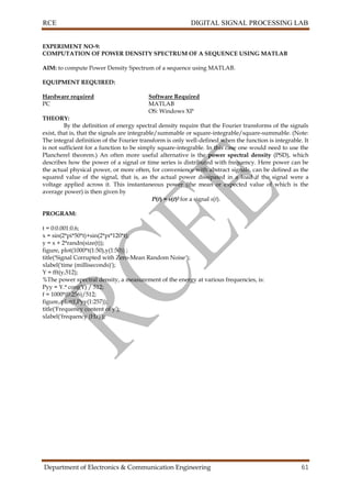
EXPERIMENT NO-10:
COMUTATION OF FFT OF 1-D SIGNAL USING MATLAB
AIM: To find the FFT of given 1-D signal and plot.
EQUIPMENT REQUIRED:
Hardware required Software Required
PC MATLAB
DSK6713 DSP Starter kit CCS Studio 3-1
USB Cable, Power Adapter OS: Windows XP
THEORY:
A fast Fourier transform (FFT) is an efficient algorithm to compute the discrete Fourier
transform (DFT) and it’s inverse. There are many distinct FFT algorithms involving a wide range of
mathematics, from simple complex-number arithmetic to group theory and number theory; this
article gives an overview of the available techniques and some of their general properties, while the
specific algorithms are described in subsidiary articles linked below.
A DFT decomposes a sequence of values into components of different frequencies. This
operation is useful in many fields (see discrete Fourier transform for properties and applications of
the transform) but computing it directly from the definition is often too slow to be practical. An FFT is
a way to compute the same result more quickly: computing a DFT of N points in the naive way, using
the definition, takes (N2) arithmetical operations, while an FFT can compute the same result in only
(N log N) operations. The difference in speed can be substantial, especially for long data sets where N
may be in the thousands or million in practice, the computation time can be reduced by several orders
of magnitude in such cases, and the improvement is roughly proportional to N / log(N).
C Program:
#include<stdio.h>
#include<math.h>
#define N 32
#define pI 3.14159
typedef struct
{
float real,imag;
}
complex;
float iobuffer[N];
float y[N];
main()
{
int i;
complex w[N];
complex x[N];
complex temp1,temp2;
int j,k,upper_leg,lower_leg,leg_diff,index,step;
for(i=0;i<N;i++)
{
iobuffer[i]=sin((2*pI*2*i)/32.0);
}
for(i=0;i<N;i++)
{
x[i].real=iobuffer[i];
x[i].imag=0.0;
}
for(i=0;i<N;i++)](https://image.slidesharecdn.com/dsplabmanual15-11-2016-190215035806/85/Dsp-lab-manual-15-11-2016-63-320.jpg)
![RCE DIGITAL SIGNAL PROCESSING LAB
Department of Electronics & Communication Engineering 64
{
w[i].real=cos((2*pI*i)/(N*2.0));
w[i].imag=sin((2*pI*i)/(N*2.0));
}
leg_diff=N/2;
step=2;
for(i=0;i<5;i++)
{
index=0;
for(j=0;j<leg_diff;j++)
{
for(upper_leg=j;upper_leg<N;upper_leg+=(2*leg_diff))
{
lower_leg=upper_leg+leg_diff;
temp1.real=(x[upper_leg]).real+(x[lower_leg]).real;
temp1.imag=(x[upper_leg]).imag+(x[lower_leg]).imag;
temp2.real=(x[upper_leg]).real-(x[lower_leg]).real;
temp2.imag=(x[upper_leg]).imag-(x[lower_leg]).imag;
(x[lower_leg]).real=temp2.real*(w[index]).real-temp2.imag*(w[index]).imag;
(x[lower_leg]).imag=temp2.real*(w[index]).imag+temp2.imag*(w[index]).real;
(x[upper_leg]).real=temp1.real;
(x[upper_leg]).imag=temp1.imag;
}
index+=step;
}
leg_diff=(leg_diff)/2;
step=step*2;
}
j=0;
for(i=1;i<(N-1);i++)
{
k=N/2;
while(k<=j)
{
j=j-k;
k=k/2;
}
j=j+k;
if(i<j)
{
temp1.real=(x[j]).real;
temp1.imag=(x[j]).imag;
(x[j]).real=(x[i]).real;
(x[j]).imag=(x[i]).imag;
(x[i]).real=temp1.real;
(x[i]).imag=temp1.imag;
}
}
for(i=0;i<N;i++)
{
y[i]=sqrt((x[i].real*x[i].real)+(x[i].imag*x[i].imag));
}
for(i=0;i<N;i++)
{
printf("%ft",y[i]);
}](https://image.slidesharecdn.com/dsplabmanual15-11-2016-190215035806/85/Dsp-lab-manual-15-11-2016-64-320.jpg)
![RCE DIGITAL SIGNAL PROCESSING LAB
Department of Electronics & Communication Engineering 66
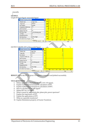
EXPERIMENT-11:
FREQUENCY RESPONSE OF ANTI IMAGING AND ANTI ALIASING FILTERS
AIM: To observe the frequency responses of anti imaging and anti aliasing filters.
EQUIPMENT REQUIRED:
Hardware required Software Required
PC MATLAB
OS: Windows XP
THEORY:
The FIR Interpolator object up samples an input by the integer up sampling factor, L,
followed by an FIR anti-imaging filter. The filter coefficients are scaled by the interpolation factor. A
poly phase interpolation structure implements the filter. The resulting discrete-time signal has a
sampling rate L times the original sampling rate. The demo versions illustrate two possible decimator
design solutions. The floating-point version model uses a cascade of three poly phase FIR decimators.
This approach reduces computation and memory requirements as compared to a single decimator by
using lower-order filters. Each decimator stage reduces the sampling rate by a factor of four. The
fixed-point version uses a five-section CIC decimator to reduce the sampling rate by the same factor
of 64. While not as flexible as a FIR decimator, the CIC decimator has the advantage of not requiring
any multiply operations. It is implemented using only additions, subtractions, and delays. Therefore,
it is a good choice for a hardware implementation where computational resources are limited.
PROGRAM FOR ANTI IMAGING FILTER
clear all;
n=0:1:1023;
x=1/4*sinc((1/4)*(n-512)).^2
i=1:1024;
y=[zeros(1,2048)];
y(2*i)=x;
f=-2:1/512:2;
h1=freqz(x,1,2*pi*f);
h2=freqz(y,1,2*pi*f);
subplot(3,1,1);
plot(f,abs(h1));
xlabel('frequency');
ylabel('magnitude');
title('frequecny response of input sequence');
subplot(3,1,2);
plot(f,abs(h2));
xlabel('frequency');
ylabel('magnitude');
title('frequency reponse of up sampled input sequence ');
p=fir1(127,.3);
xf=filter(p,1,y);
h4=freqz(xf,1,2*pi*f);
subplot(3,1,3);
plot(f,abs(h4));
title('frequency response of output of an anti imanaging filter');
xlabel('frequency');
ylabel('magnitude');](https://image.slidesharecdn.com/dsplabmanual15-11-2016-190215035806/85/Dsp-lab-manual-15-11-2016-66-320.jpg)
![RCE DIGITAL SIGNAL PROCESSING LAB
Department of Electronics & Communication Engineering 67
OUTPUT:
PROGRAM FOR ANTI ALIASING FILTER:
clear all;
F=input('enter the highest normalized frequency component');
D=input('emter the dicimation factor');
n=0:1:1024;
xd=(F/2*sinc(F/2)*(n-512)).^2;
f=-2:1/512:2;
h1=freqz(xd,1,pi*f);
subplot(3,1,1);
plot(f,abs(h1));
xlabel('frequency');
ylabel('magnitude');
title('frequency response of input sequence');
if(F*D<=1)
xd1=F/2*sinc(F/2*(n-512)*D).^2;
h2=freqz(xd1,1,pi*f*D);
subplot(3,1,3)
plot(f,abs(h2));
axis([-2 2 0 1]);
h2=freqz(xd1,1,pi*f*D);
subplot(3,1,2);
plot(f*D,abs(h2));
axis([-2*D 2*D 0 1]);
else
p=fir1(127,1/D);
xf=filter(p,1,xd);
h4=freqz(xf,1,pi*f);
subplot(3,1,3);
plot(f,abs(h4));
title('FREQUENCY RESPONSE OF OUTPUT OF ANTI ALIASING FILTER');
xlabel('frequency');
ylabel('magnitude');
i=1:1:1024/D;](https://image.slidesharecdn.com/dsplabmanual15-11-2016-190215035806/85/Dsp-lab-manual-15-11-2016-67-320.jpg)
![RCE DIGITAL SIGNAL PROCESSING LAB
Department of Electronics & Communication Engineering 69
PROCEDURE FOR HARDWARE EXECUTION
I. Consignment list
1. A main board of DSP6713 -1No
2. Power Supply 5V, 3A. - 1No
3. USB Programmer-1No
4. USB Cable -1No
4. Head Phone with MIC -1No
5. Audio Jack -3No [1+2]
6. Sample and Syllabus Programs CD -1No
7. DSP Lab Manual -1No
II. Introduction of main board
1. USB2.0 CY7C68013-56PVC, compatible with USB2.0 and USB1.1, including 8051
2. DSP TMS320C6713 TQFP-208 Package Device with, 4 layers board
3. SDRAM MT48LC4M16A2 1meg*16 *4 bank micron
4. FLASH AM29LV800B 8Mbit1Mbyte of AMD
5. RESET chip specialize for reset with button for manually reset
6. POWER supply externally, special 5V, 3.3V, 1.6V chip for steady voltage with remaining for other
devices.
7. EEPROM 24LC64 for download of USB firmware
8. CPLD XC95144XL
9. AIC TLV320AIC23B sampling with 8-96KHZ, 4 channels
III. The setup of XDS510 USB emulator in CCS V3.1
1. Install CCS V3.1 software according to the Custom Install default Custom Install_could changes the
installation directory. Following is an example of install the software under C disk root directory.
2. Install USB Emulator choose to install directory from CCS v3.1 that is if CCSv3.1 is installed in C: /
CCStudio_v3.1 directory, then install the USB emulator driver in this directory.
3. Replace TIXDS510_Connection.xml file [From CCStudio_v3.1driversTargetDB connection
with the TIXDS510_Connection.xml in xds510_setup directory.]
Procedure to Setup Emulator:
Start->Program->Texas Instrument-> Code Composer Studio 3.1 ->Setup Code Composer Studio
v3.1, the window of Code Composer Studio Setup will show up.](https://image.slidesharecdn.com/dsplabmanual15-11-2016-190215035806/85/Dsp-lab-manual-15-11-2016-69-320.jpg)
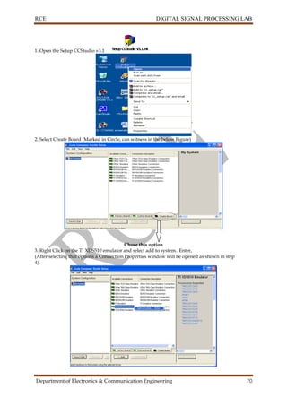
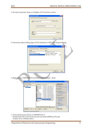
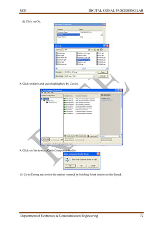
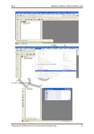


![Eee iv-microcontrollers [10 es42]-notes](https://cdn.slidesharecdn.com/ss_thumbnails/eee-iv-microcontrollers10es42-notes-190903091207-thumbnail.jpg?width=640&height=640&fit=bounds)
![Eee iv-microcontrollers [10 es42]-assignment](https://cdn.slidesharecdn.com/ss_thumbnails/eee-iv-microcontrollers10es42-assignment-190903091039-thumbnail.jpg?width=640&height=640&fit=bounds)


