Downloaded 24 times
![Comparison with other similar works:
Sr.
No.
Group Name
Adder Type
Technology
Adder Delay
Power
Consumption
Power Delay Product
1
[1] University of Waterloo
Department of ECE
16 bit Kogge
Stone
FPGA 45nM
419ps
13.29mW
5.57E-12
2
This work
16 bit Brent
Kung Adder
NCSU 45nM Free PDK
ASIC
359ps
6.73mW
2.41E-12
3
[4] University of Texas,
Tyler Department of EE
16 bit Kogge
Stone
Spartan 3e 90nM
6.286ns
--
--
4
[2] VIT University, Vellore
16 bit Kogge
Stone
SPARTAN 3e 90nM
599ns
46.16uW
2.76E-11
5
[2] VIT University, Vellore
16 bit Brent
Kung Adder
Spartan 3e 90nM
762ns
32.465uW
2.47E-11
8
[5] University of
Wisconsin, Madison
16 bit Ripple
Carry Adder
LSI Logic 110nM ASIC
2.59ns
--
--
9
[5] University of
Wisconsin, Madison
16 bit Carry
Lookahead
Adder
LSI Logic 110nM ASIC
1.09ns
--
--
6
[3] Concordia University
Department of ECS
16 bit Brent
Kung Adder
Virtex 2 130nM
26.94ns
1.15W
3.10E-08
7
[3] Concordia University
Department of ECS
16 bit Kogge
Stone
Virtex 2 130nM
25.59ns
1.5546W
3.97E-08
Column1
Work done as a student at the University of Minnesota, Twin Cities by Nirav Desai desai.nirav.12.09@gmail.com](https://image.slidesharecdn.com/brentkungadderpaperupdated-140302033508-phpapp02/75/Design-of-a-high-speed-low-power-Brent-Kung-Adder-in-45nM-CMOS-19-2048.jpg)
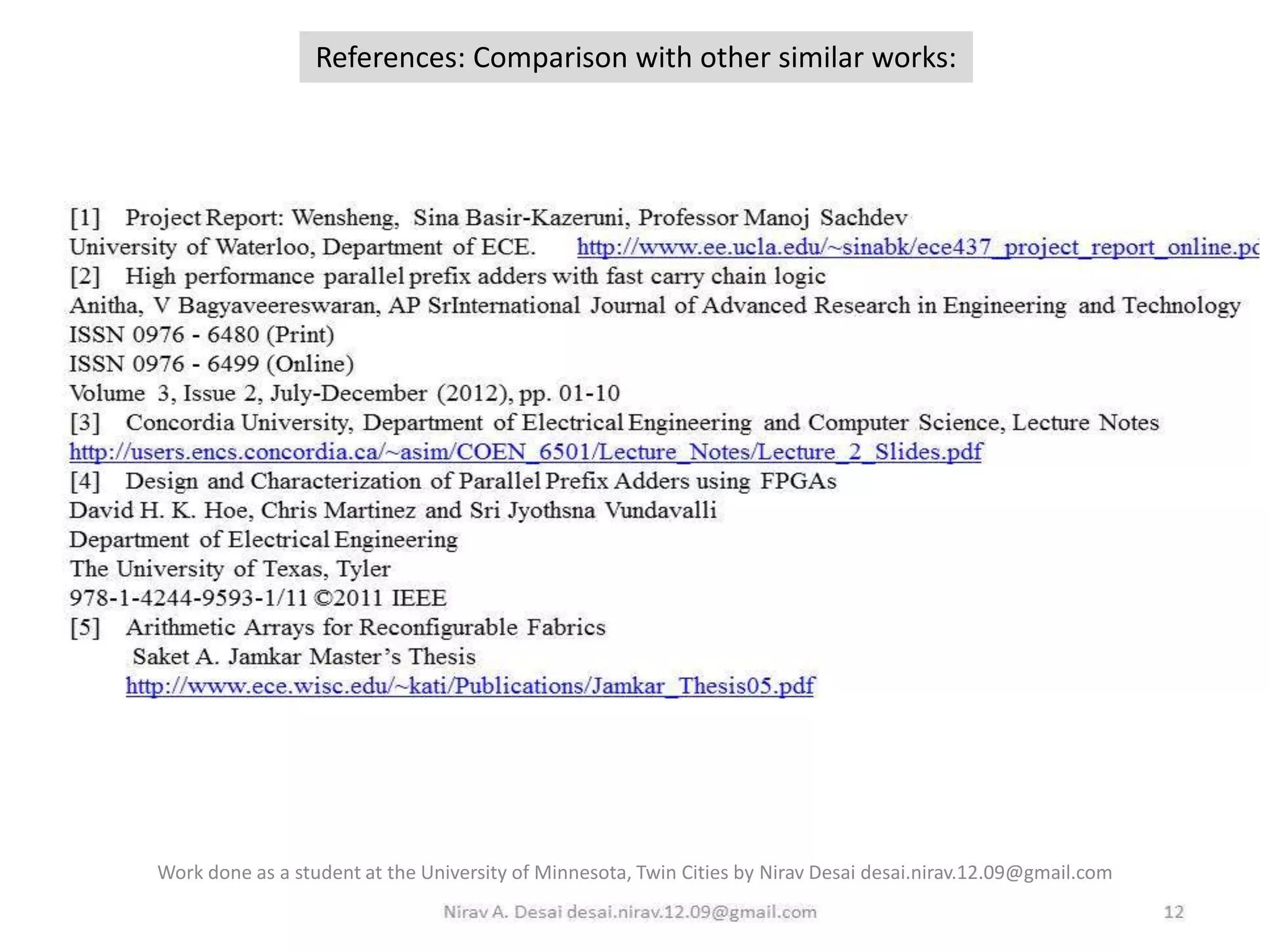

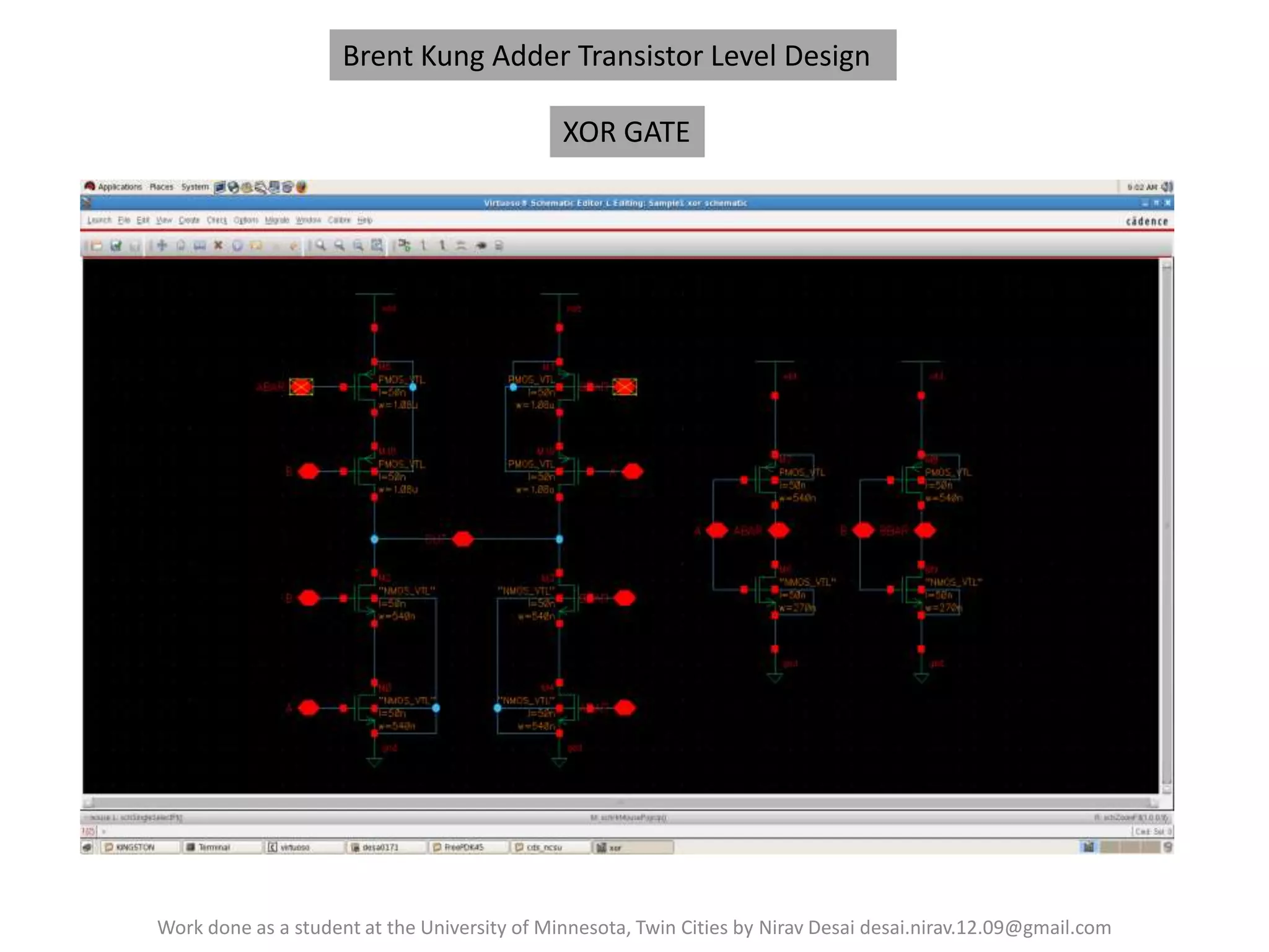
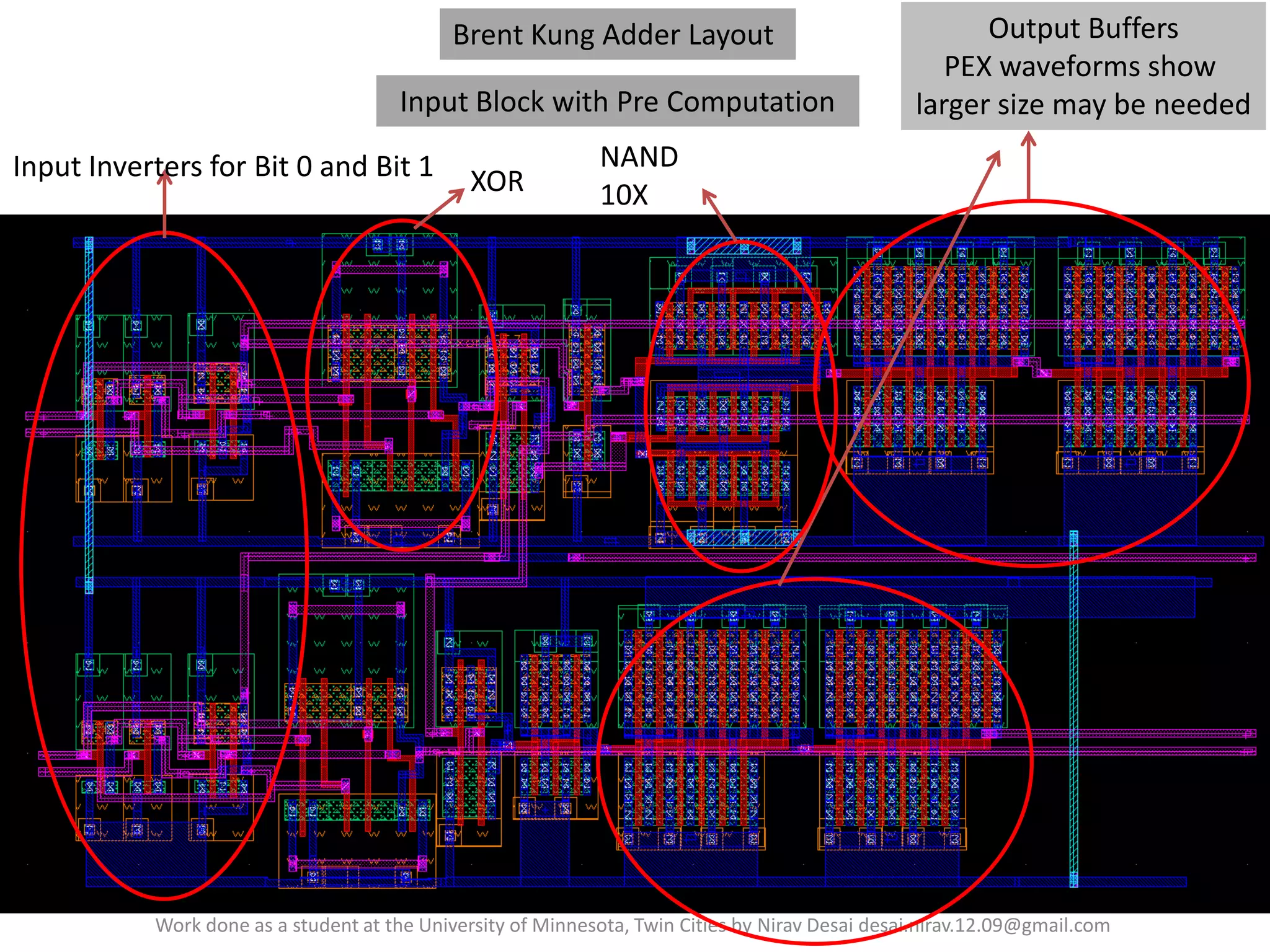
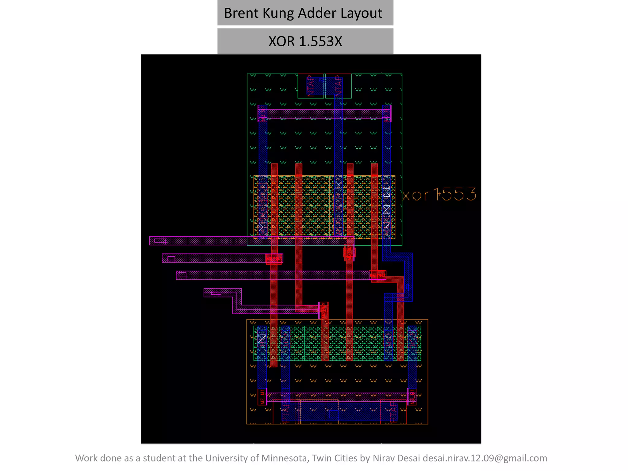
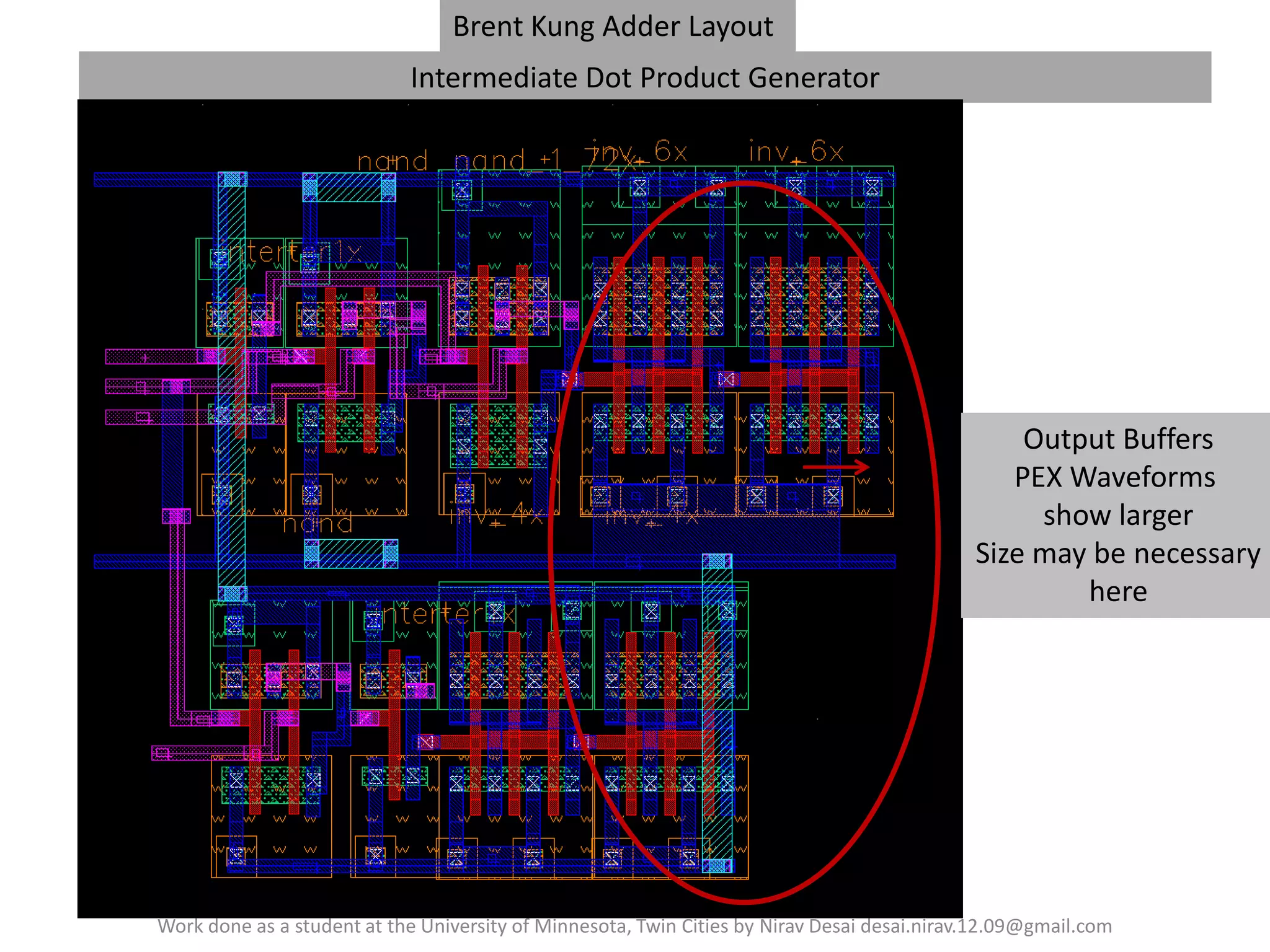
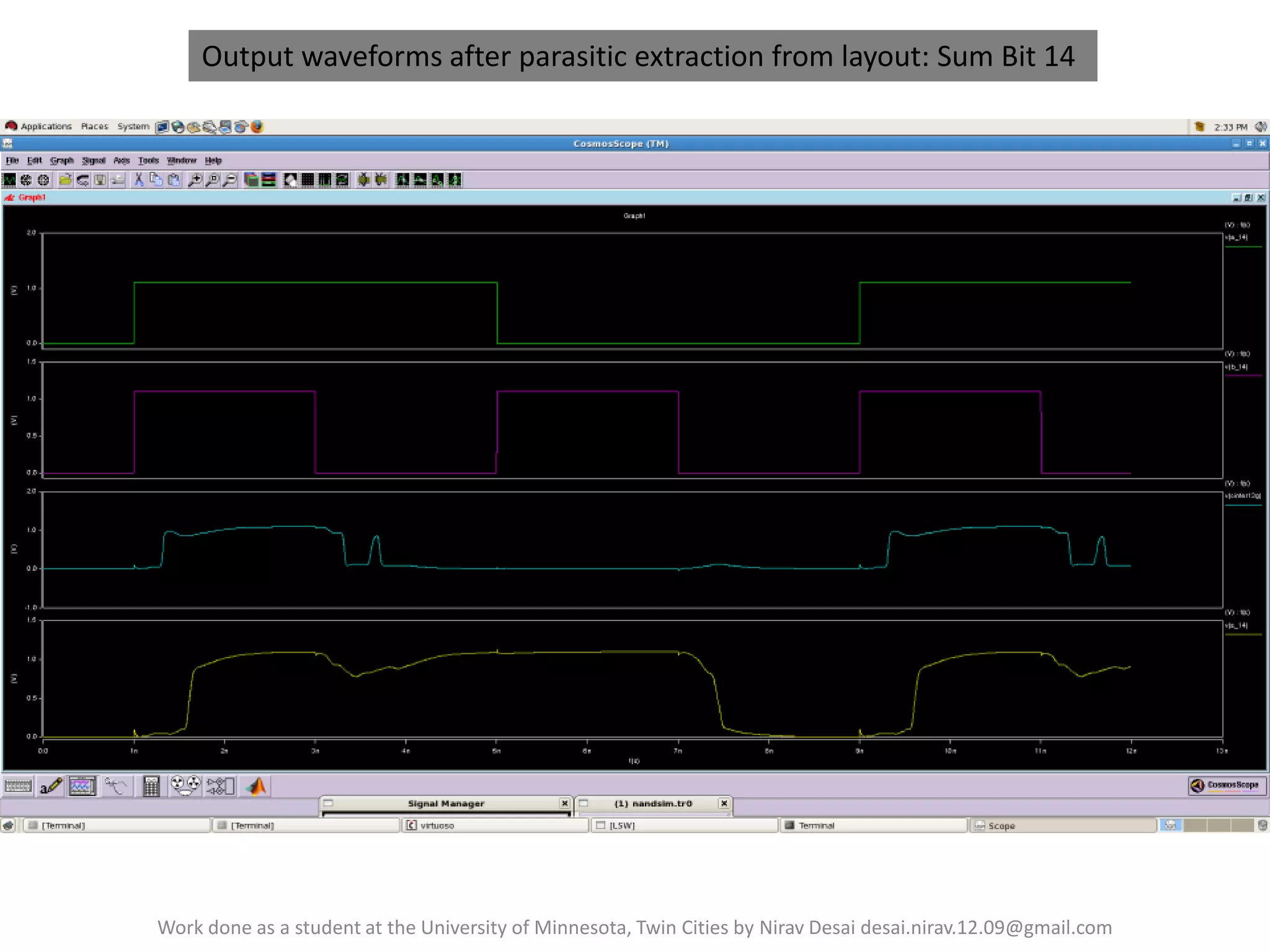
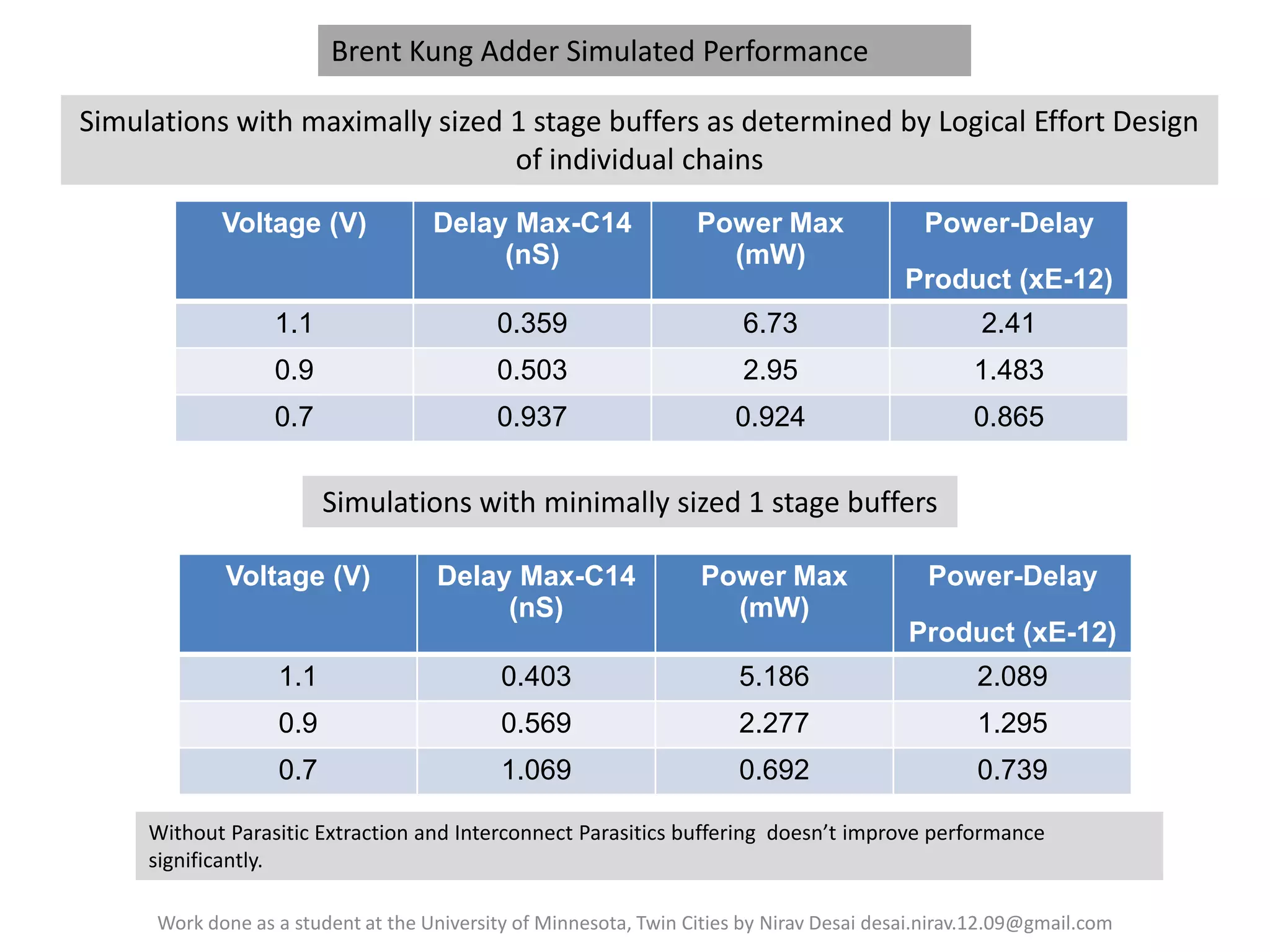
This document discusses the design and optimization of a 16-bit Brent Kung adder implemented in CMOS technology, focusing on reducing power dissipation while meeting speed requirements. It provides detailed specifications and performance comparisons to other adder types, including simulations and layout designs. The work is attributed to Nirav Desai, a student at the University of Minnesota, Twin Cities.


![Vibe Coding vs. Spec-Driven Development [Free Meetup]](https://cdn.slidesharecdn.com/ss_thumbnails/vibecodingvsspecdrivendevelopment-251209105622-43f455e7-thumbnail.jpg?width=640&height=640&fit=bounds)


