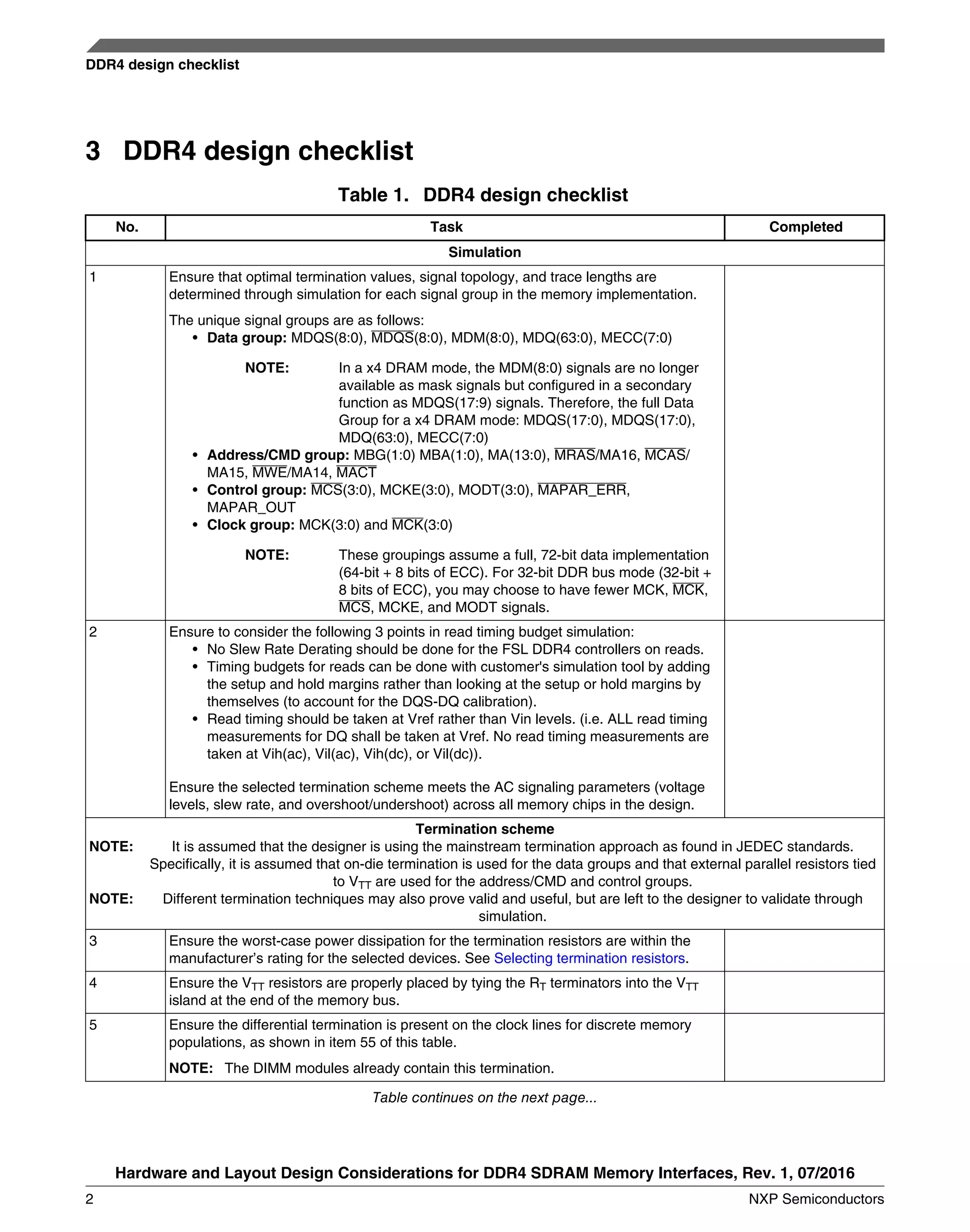
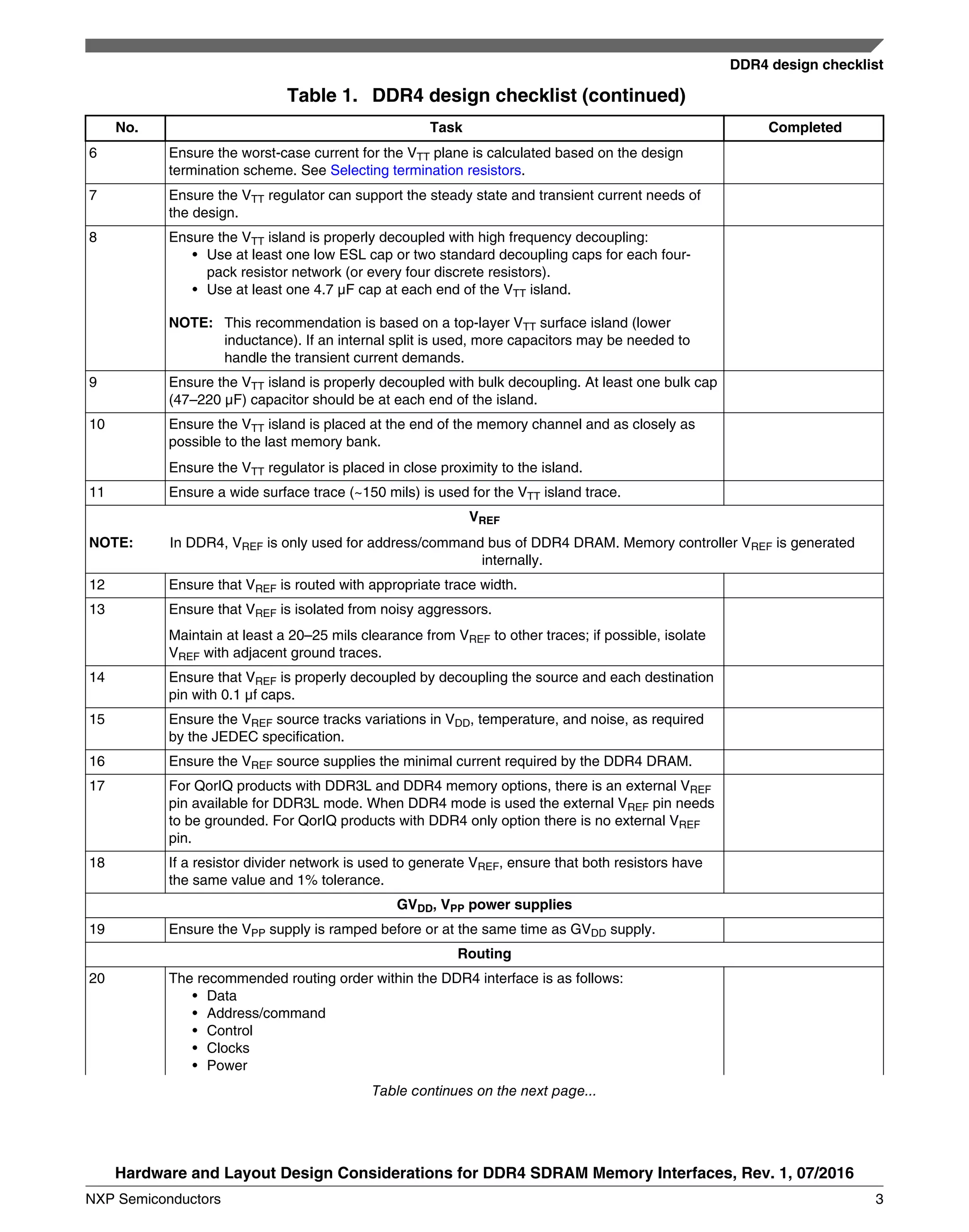
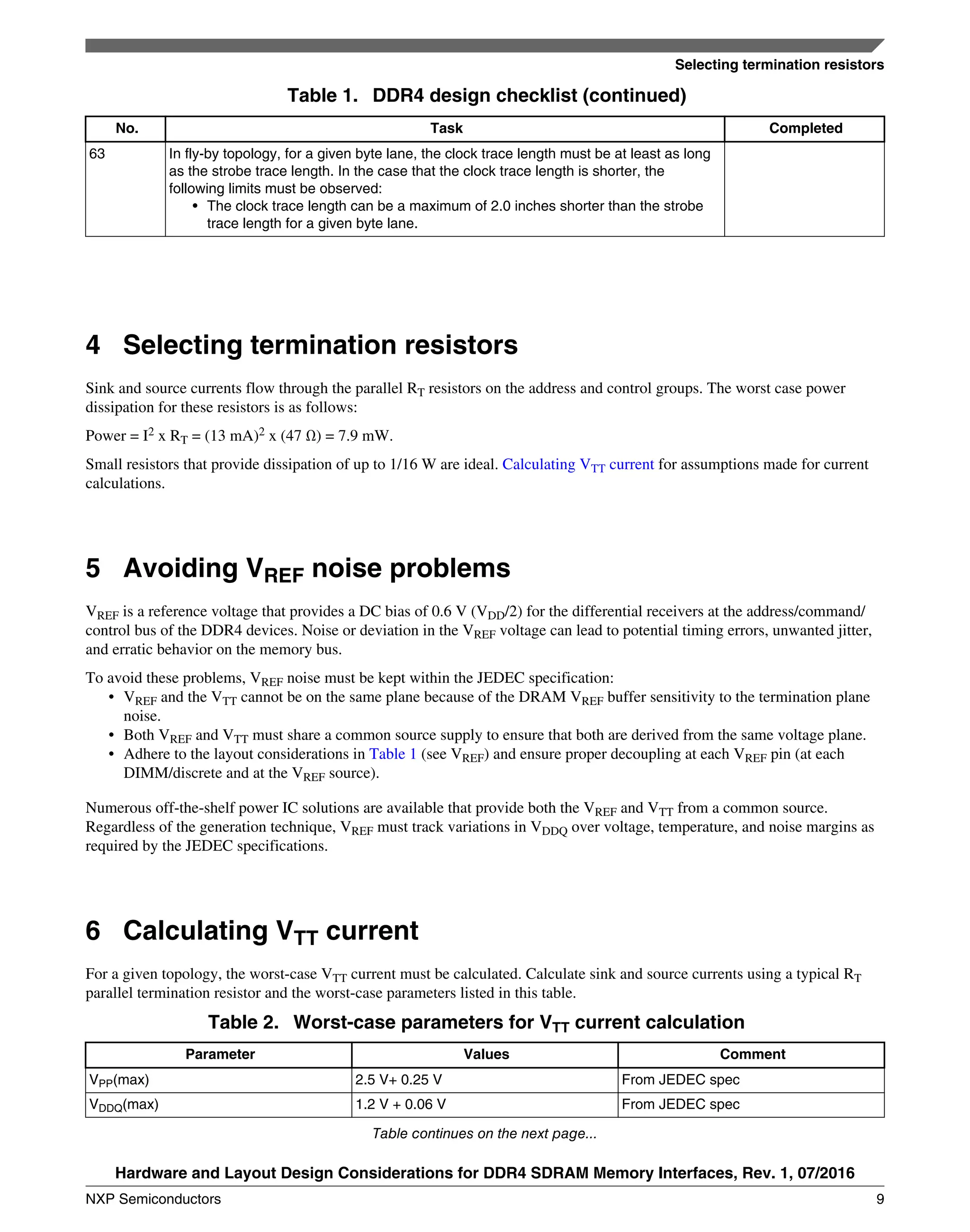
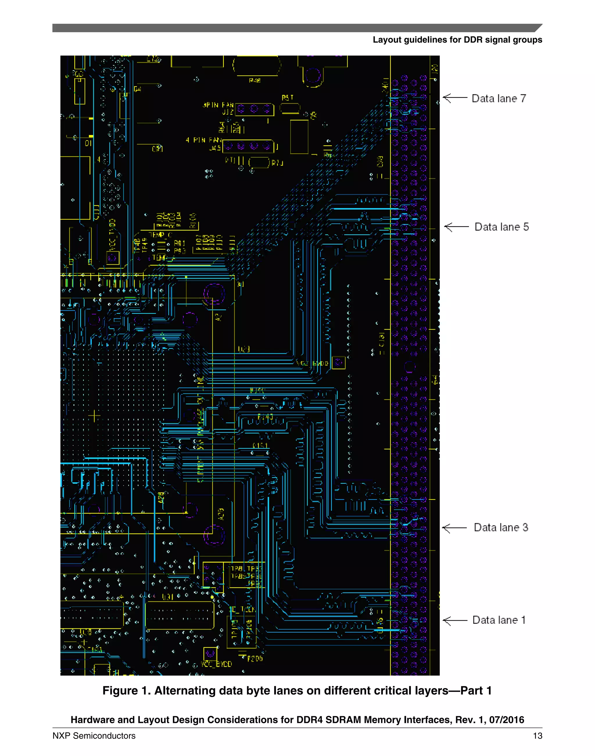
This document provides guidelines for hardware engineers implementing a DDR4 memory subsystem. It recommends using simulation to optimize the design for signal integrity and timing and provides a checklist of key design considerations. These include routing the data and command/address signals in separate groups, using fly-by routing topologies, matching trace lengths, and properly terminating the various signal groups. Guidelines are given for impedance values and trace spacings for the different signal types.


![Table 1. DDR4 design checklist (continued)
No. Task Completed
• Bit-swap is only allowed within a nibble.
• Bit-swap across two nibbles is not allowed.
• Bit-swap across byte lanes is not allowed.
• For 32-bit or 16-bit DDR4 data bus, in the ECC byte lane only, the DQ[0], and
DQ[1] bit-swap is not allowed.
28 Ensure that each data lane properly is trace-matched to within 20 mils of its respective
differential data strobe.
• Ensure the trace matching for parts with operational data rates of higher than
1600 MT/s is within +/-5 mils.
29 When adding trace lengths to any of the DDR4 signal groups, ensure that there is at
least 25 mils between serpentine loops that are in parallel.
30 MDQS/MDQS considerations:
• Match all segment lengths between differential pairs along the entire length of the
pair. Trace match the MDQS/MDQS pair to be within +/-5 mils.
• Maintain constant line impedance along the routing path by maintaining the
required line width and trace separation for the given stackup.
• Avoid routing differential pairs adjacent to noisy signal lines or high-speed
switching devices such as clock chips.
• Differential impedance 75–95 Ω
• Differential impedance 90-95 Ω for parts with operational speeds of higher than
1600 MT/s
• Diff Gap = 4–5 mils (as DQS signals are not true differential, also known as
“pseudo differential”)
• Diff Gap = 5–8 mils, for parts with operational speeds of higher than 1600 MT/s.
Choose one of the following options to select the impedances and spacings for MDQS/
MDQS differential strobes.
Option #1 (wider traces—lower trace impedance):
• Single-ended impedance 40 Ω. The lower impedance allows traces to be slightly
closer with less cross-talk.
• Utilize wider traces if stackup allows (7–8 mils).
• Spacing to other data signals = 2x
• If not routed on the same layer as its associated data, then 4x spacing.
Option #2 (smaller traces—higher trace impedance):
• Single-ended impedance = 50 Ω
• Smaller trace widths (5–6 mils) can be used.
• Spacing between like signals (other data) should increase to 3x (for 5 mils) or
2.5x (for 6 mils), respectively.
• Do not divide the two halves of the diff pair between layers. Route the MDQS/
MDQS pair on the same critical layer as its associated data lane.
Routing address/command/control/clock bus
31 Ensure fly-by topology is used for address/command/control and clock groups. The
routing in fly-by topology should go from chip 0 to chip n and can be in the order that is
most convenient for the board design. The fly-by topology routing of address/command/
control and clock groups must end at the termination resistors that are after chip n.
Choose one of the following options to select the impedances and spacings for the
DDR4 address/command/control group.
Option #1 (wider traces—lower trace impedance):
• Single-ended impedance = 40 Ω. The lower impedance allows traces to be
slightly closer with less cross-talk.
• Utilize wider traces if stackup allows (7–8 mils).
Table continues on the next page...
DDR4 design checklist
Hardware and Layout Design Considerations for DDR4 SDRAM Memory Interfaces, Rev. 1, 07/2016
NXP Semiconductors 5](https://image.slidesharecdn.com/an5097-220810054537-11c7793f/75/AN5097-pdf-5-2048.jpg)



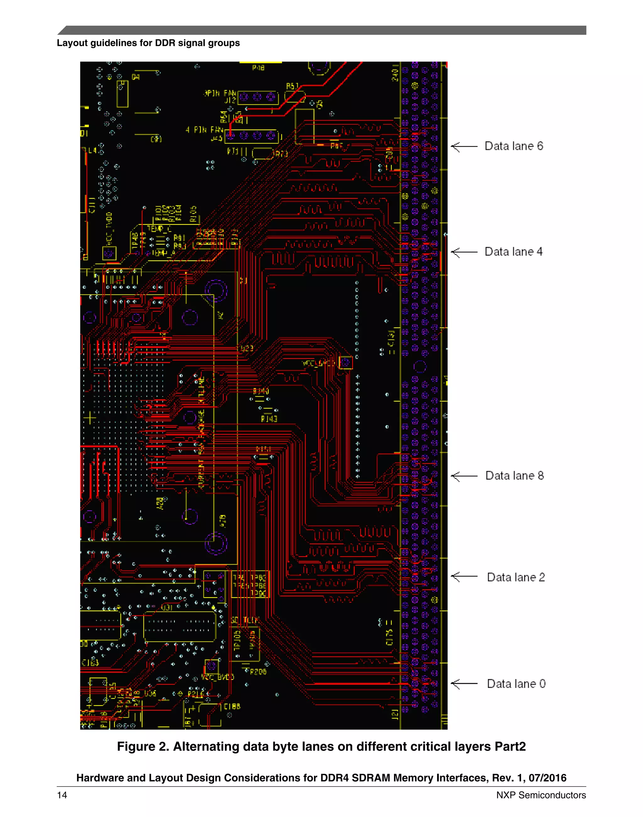
![7.3 Routing DDR data signals
The DDR interface data signals (MDQ[0:63], MDQS[0:8], MDM[0:8], and MECC[0:7]) are source-synchronous signals by
which memory and the controller capture the data using the data strobe rather than the clock itself. When transferring data,
both edges of the strobe are used to achieve the 2x data rate.
An associated data strobe (DQS and DQS) and data mask (DM) comprise each data byte lane. This 11-bit signal lane
relationship is crucial for routing (see Table 3). When length matching, the critical item is the variance of the signal lengths
within a given byte lane to its strobe. Length matching across all bytes lanes is also important and must meet the tDQSS
parameter as specified by JEDEC. This is also commonly referred to as the write data delay window. Typically, this timing is
considerably more relaxed than the timing of the individual byte lanes themselves.
Table 3. Byte lane to data strobe and data mask mapping
Data Data strobe Data mask x4 mode data strobe Lane number
MDQ[0:7] MDQS0, MDQS0 MDM0 MDQS9, MDQS9 Lane 0
MDQ[8:15] MDQS1, MDQS1 MDM1 MDQS10, MDQS10 Lane 1
MDQ[16:23] MDQS2, MDQS2 MDM2 MDQS11, MDQS11 Lane 2
MDQ[24:31] MDQS3, MDQS3 MDM3 MDQS12, MDQS12 Lane 3
MDQ[32:39] MDQS4, MDQS4 MDM4 MDQS13, MDQS13 Lane 4
MDQ[40:47] MDQS5, MDQS5 MDM5 MDQS4, MDQS14 Lane 5
MDQ[48:55] MDQS6, MDQS6 MDM6 MDQS5, MDQS15 Lane 6
MDQ[56:63] MDQS7, MDQS7 MDM7 MDQS6, MDQS16 Lane 7
MECC[0:7] MDQS8, MDQS8 MDM8 MDQS7, MDQS17 Lane 8
NOTE
When routing, each row (that is, the 11-bit signal group) must be treated as a trace-
matched group.
When x4 DRAM mode is available and used, the data mask signals are not available.
Instead the strobe signals listed under the x4 Mode Data Strobe column are the strobes
for the second nibble of each byte lane.
7.4 DDR signal groups layout recommendations
This table lists the layout recommendations for DDR signal groups and the benefit of following each recommendation.
Table 4. DDR signal groups layout recommendations
Recommendation Benefit
Route each data lane adjacent to a solid ground reference for
the entire route to provide the lowest inductance for the return
currents.
Provides the optimal signal integrity of the data interface
NOTE: This concern is especially critical in designs that
target the top-end interface speed, because the data
switches at 2x the applied clock.
Table continues on the next page...
Layout guidelines for DDR signal groups
Hardware and Layout Design Considerations for DDR4 SDRAM Memory Interfaces, Rev. 1, 07/2016
NXP Semiconductors 11](https://image.slidesharecdn.com/an5097-220810054537-11c7793f/75/AN5097-pdf-11-2048.jpg)







![Implementation of these DRAM reset requirements for RDIMM can be achieved via some combination of software and
hardware. Below is an example of implementing the DRAM reset requirements for RDIMM. It is important to note that this
is not the only way to implement the required DRAM reset timing or the recommended way. This is simply an example.
In QorIQ products (except LS1012A and LS1024A):
• The CKE signal remains low until the memory controller is enabled (DDR_SDRAM_CFG[MEM_EN] = 1).
• Before the memory controller is enabled, all DDR registers must be configured.
• The DDR clock starts running when any chip select is enabled (CSn_CONFIG[CSn_EN] = 1).
Assert the DRAM reset signal at the same time the HRESET signal is asserted. De-asserting the DRAM rest signal needs to
be timed to occur after clocks are present while the CKE signal is low. In other words, the DRAM reset signal must be de-
asserted after software enables any chip select (CSn_CONFIG[CSn_EN] = 1) and before software enables the memory
controller (DDR_SDRAM_CFG[MEM_EN] = 1). Apply a large enough delay between chip select enable and memory
controller enable. Then observe the HRESET, DRAM reset, MCKn, and CKEn signals on an oscilloscope, and time the de-
assertion of the DRAM reset to fall after MCKn is present and before the CKEn signal goes to logic high level.
Hardware and Layout Design Considerations for DDR4 SDRAM Memory Interfaces, Rev. 1, 07/2016
NXP Semiconductors 25](https://image.slidesharecdn.com/an5097-220810054537-11c7793f/75/AN5097-pdf-25-2048.jpg)
