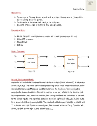
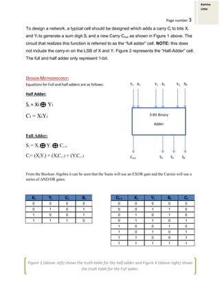
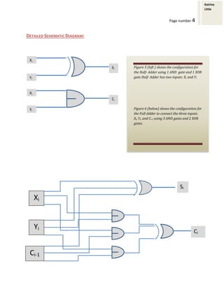
The document describes the design and implementation of a three-bit binary adder using discrete gates on an FPGA board. It details the iterative cell design technique, using full and half adder schematics, along with Verilog code representations. A test plan is included to validate the design against truth tables and ensure correct operation.


![Katrina
Little
Page number 5
VERILOG REPRESENTATION OF SCHEMATIC:
module(X,Y,S,C0;
input [2:0]X;
input [2:0]Y;
output [2:0]S;
output C;
wire[2:0] X;
wire[2:0]Y;
wire[2:0]S;
assign S[0] = X[0]^Y[0];
assign S[1] = (X[0]&Y[0]^(X[1]^Y[1]);
assign S[2] =(((X[0]&Y[0])&X[1])) + ((X[0]&Y[0])&Y[1]) +(X[1]&Y[1]))^(X[2]^Y[2]);
assign C = ((((X[0]&Y[0])&X[1]) + ((X[0]&Y[0])&Y[1]) + ((X[1]&Y[1])&X[2]) + ((((X[0]&Y[0])&X[1])
+((X[0]&Y[0])&Y[1]) + (X[1]&Y[1])&Y[2]) +(X[2]&Y[2]);
endmodule
Input/Output Switch LED Pin #
X[0] SW0 38
X[2] SW2 29
Y[0] SW5 12
Y[2] SW7 6
S[0] LED0 15
S[2] LED2 8
Cout LED7 2
Figure 7 (left) displays the Pin connections
for the Switches and LED’s of the inputs and
outputs of the Schematics.](https://image.slidesharecdn.com/lab4-3-bitbinaryadder-180723164618/85/Lab-4-Three-Bit-Binary-Adder-5-320.jpg)


![SEQUENTIAL CIRCUITS [Flip-flops and Latches]](https://cdn.slidesharecdn.com/ss_thumbnails/sequentialcircuits-211217082412-thumbnail.jpg?width=640&height=640&fit=bounds)