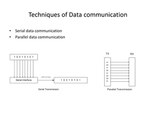
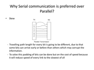
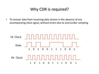
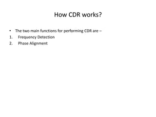
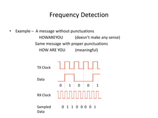
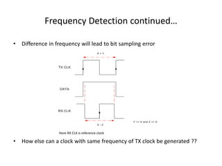
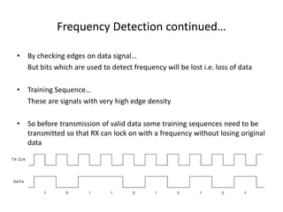
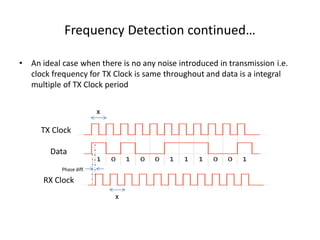
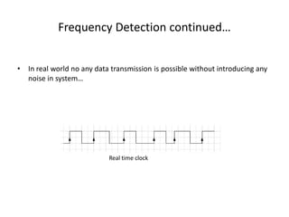
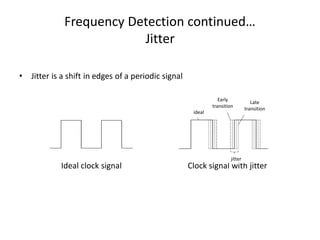
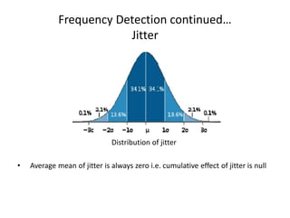
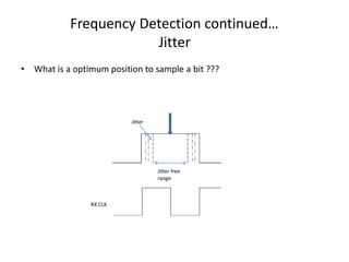
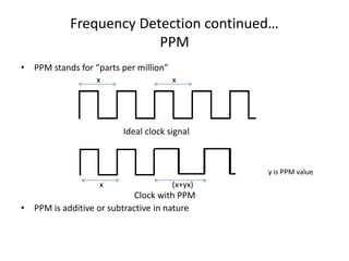
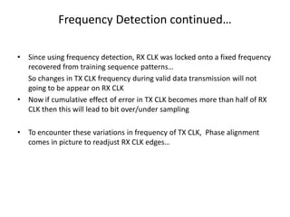
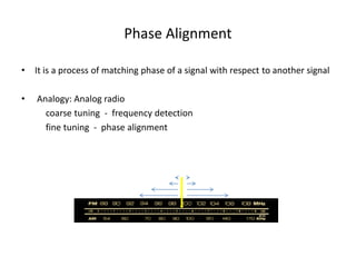
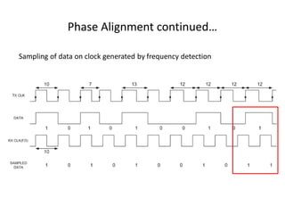
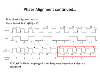
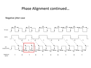
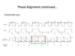
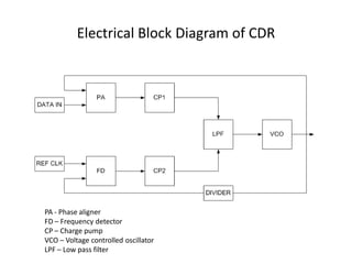
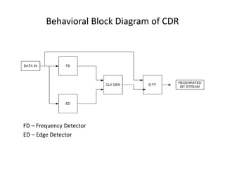
Behavioral Modeling of Clock
and Data Recovery
ARROW DEVICES
Presented by – Deepak Nagaria
Agenda
• Techniques of Data communication
• Why Serial communication is preferred over Parallel?
• What is Clock and Data recovery?
• Why CDR is required?
• How CDR works?
Frequency Detection
Jitter
PPM
Phase Alignment
Why encoding is needed?
• Behavioral flow of CDR
Techniques of Data communication
• Serial data communication
• Parallel data communication
Why Serial communication is preferred over
Parallel?
• Skew
- Travelling path length for every bit is going to be different, due to that
some bits can arrive early or before than others which may corrupt the
information.
- To solve this padding of bits can be done but on the cost of speed because
it will reduce speed of every link to the slowest of all
Why Serial communication is preferred over
Parallel continued…
• Inter symbol interference and Cross talk
Due to several parallel links ISI and Cross talk introduced in system which
is more severe as length of link increased. So this limits length of a
connection.
• Limitation of I/O pin count.
What is Clock and Data recovery?
• Most of the high speed serial interfaces do not have any accompanying
clock
• Receiver needs to “recover” a clock in order to sample data on serial lines
• In order to recover the sampling clock, receiver needs a reference clock of
approximately same frequency
• To generate the recovered clock, the receiver needs to phase align the
reference clock to the transitions on the incoming data stream
• Sampling of that incoming data signal with recovered clock to generate a
bit stream is called as Data recovery.
Why CDR is required?
• To recover data from incoming data stream in the absence of any
accompanying clock signal, without errors due to over/under sampling
TX
RX
1 0 1 0 0 1 1 1 0 0 1
How CDR works?
• The two main functions for performing CDR are –
1. Frequency Detection
2. Phase Alignment
Frequency Detection
• Example – A message without punctuations
HOWAREYOU (doesn’t make any sense)
Same message with proper punctuations
HOW ARE YOU (meaningful)
TX Clock
Data
RX Clock
Sampled 0 1 1 0 0 0 0 1
Data
0 001 1
Frequency Detection continued…
• How incoming data can be sampled correctly ???
By sampling it with same frequency on which it was transmitted…
• So a reference clock on RX can be generated having same frequency as of
TX ???
No it is not possible to generate two clocks having exactly same frequency
by using two different clock generators having same specifications
Also it is not possible to generate a clock with precise frequency
Frequency Detection continued…
• Difference in frequency will lead to bit sampling error
Here RX CLK is reference clock
• How else can a clock with same frequency of TX clock be generated ??
Frequency Detection continued…
• By checking edges on data signal…
But bits which are used to detect frequency will be lost i.e. loss of data
• Training Sequence…
These are signals with very high edge density
• So before transmission of valid data some training sequences need to be
transmitted so that RX can lock on with a frequency without losing original
data
Frequency Detection continued…
• An ideal case when there is no any noise introduced in transmission i.e.
clock frequency for TX Clock is same throughout and data is a integral
multiple of TX Clock period
TX Clock
RX Clock
Data
x
x
Phase diff.
Frequency Detection continued…
• In real world no any data transmission is possible without introducing any
noise in system…
Clock with noise
Real time clock
Frequency Detection continued…
• The two noise(error) factors which affects most to any serial data
communication system are –
I. Jitter
II. PPM
Frequency Detection continued…
Jitter
• Jitter is a shift in edges of a periodic signal
Ideal clock signal Clock signal with jitter
ideal
Early
transition
Late
transition
jitter
Frequency Detection continued…
Jitter
Distribution of jitter
• Average mean of jitter is always zero i.e. cumulative effect of jitter is null
Frequency Detection continued…
Jitter
• What is a optimum position to sample a bit ???
Jitter free
range
Jitter
RX CLK
Frequency Detection continued…
PPM
• PPM stands for “parts per million”
Ideal clock signal
Clock with PPM
• PPM is additive or subtractive in nature
x x
x (x+yx)
y is PPM value
Frequency Detection continued…
• Since using frequency detection, RX CLK was locked onto a fixed frequency
recovered from training sequence patterns…
So changes in TX CLK frequency during valid data transmission will not
going to be appear on RX CLK
• Now if cumulative effect of error in TX CLK becomes more than half of RX
CLK then this will lead to bit over/under sampling
• To encounter these variations in frequency of TX CLK, Phase alignment
comes in picture to readjust RX CLK edges…
Phase Alignment
• It is a process of matching phase of a signal with respect to another signal
• Analogy: Analog radio
coarse tuning - frequency detection
fine tuning - phase alignment
Phase Alignment continued…
Sampling of data on clock generated by frequency detection
Phase Alignment continued…
Phase Alignment Rules
• If a transition is detected on line then make level of RX CLK(FD+PD) = 1
• If RX CLK(FD) period is completed after a posedge on RX CLK(FD+PD) and
no any transition is detected on line then assert posedge of RX
CLK(FD+PD)
Phase Alignment continued…
How phase alignment works
Clock Period RX CLK(FD) = 10
RX CLK(FD+PD) is sampling clk after frequency detection and phase
alignment
Phase Alignment continued…
Negative jitter case
Phase Alignment continued…
Positive jitter case
Phase Alignment continued…
• What if a long sequence of identical bit occur on data???
• To solve this problem we do various types of encoding on bit sequence
before transmitting it, which limits the number of consecutive identical
bits to a certain level
• For ex –
In M-PHY before putting data on line, it processed with 8B10B encoding
Electrical Block Diagram of CDR
PA - Phase aligner
FD – Frequency detector
CP – Charge pump
VCO – Voltage controlled oscillator
LPF – Low pass filter
Behavioral Block Diagram of CDR
FD – Frequency Detector
ED – Edge Detector
Behavioral Block Diagram of CDR continued…
Flow chart for clock generation after phase alignment -
ED – Edge Detection
FD – Frequency
Detection
Questions ???
Thank you

Behavioral modeling of Clock/Data Recovery

  • 1.
    Behavioral Modeling ofClock and Data Recovery ARROW DEVICES Presented by – Deepak Nagaria
  • 2.
    Agenda • Techniques ofData communication • Why Serial communication is preferred over Parallel? • What is Clock and Data recovery? • Why CDR is required? • How CDR works? Frequency Detection Jitter PPM Phase Alignment Why encoding is needed? • Behavioral flow of CDR
  • 3.
    Techniques of Datacommunication • Serial data communication • Parallel data communication
  • 4.
    Why Serial communicationis preferred over Parallel? • Skew - Travelling path length for every bit is going to be different, due to that some bits can arrive early or before than others which may corrupt the information. - To solve this padding of bits can be done but on the cost of speed because it will reduce speed of every link to the slowest of all
  • 5.
    Why Serial communicationis preferred over Parallel continued… • Inter symbol interference and Cross talk Due to several parallel links ISI and Cross talk introduced in system which is more severe as length of link increased. So this limits length of a connection. • Limitation of I/O pin count.
  • 6.
    What is Clockand Data recovery? • Most of the high speed serial interfaces do not have any accompanying clock • Receiver needs to “recover” a clock in order to sample data on serial lines • In order to recover the sampling clock, receiver needs a reference clock of approximately same frequency • To generate the recovered clock, the receiver needs to phase align the reference clock to the transitions on the incoming data stream • Sampling of that incoming data signal with recovered clock to generate a bit stream is called as Data recovery.
  • 7.
    Why CDR isrequired? • To recover data from incoming data stream in the absence of any accompanying clock signal, without errors due to over/under sampling TX RX 1 0 1 0 0 1 1 1 0 0 1
  • 8.
    How CDR works? •The two main functions for performing CDR are – 1. Frequency Detection 2. Phase Alignment
  • 9.
    Frequency Detection • Example– A message without punctuations HOWAREYOU (doesn’t make any sense) Same message with proper punctuations HOW ARE YOU (meaningful) TX Clock Data RX Clock Sampled 0 1 1 0 0 0 0 1 Data 0 001 1
  • 10.
    Frequency Detection continued… •How incoming data can be sampled correctly ??? By sampling it with same frequency on which it was transmitted… • So a reference clock on RX can be generated having same frequency as of TX ??? No it is not possible to generate two clocks having exactly same frequency by using two different clock generators having same specifications Also it is not possible to generate a clock with precise frequency
  • 11.
    Frequency Detection continued… •Difference in frequency will lead to bit sampling error Here RX CLK is reference clock • How else can a clock with same frequency of TX clock be generated ??
  • 12.
    Frequency Detection continued… •By checking edges on data signal… But bits which are used to detect frequency will be lost i.e. loss of data • Training Sequence… These are signals with very high edge density • So before transmission of valid data some training sequences need to be transmitted so that RX can lock on with a frequency without losing original data
  • 13.
    Frequency Detection continued… •An ideal case when there is no any noise introduced in transmission i.e. clock frequency for TX Clock is same throughout and data is a integral multiple of TX Clock period TX Clock RX Clock Data x x Phase diff.
  • 14.
    Frequency Detection continued… •In real world no any data transmission is possible without introducing any noise in system… Clock with noise Real time clock
  • 15.
    Frequency Detection continued… •The two noise(error) factors which affects most to any serial data communication system are – I. Jitter II. PPM
  • 16.
    Frequency Detection continued… Jitter •Jitter is a shift in edges of a periodic signal Ideal clock signal Clock signal with jitter ideal Early transition Late transition jitter
  • 17.
    Frequency Detection continued… Jitter Distributionof jitter • Average mean of jitter is always zero i.e. cumulative effect of jitter is null
  • 18.
    Frequency Detection continued… Jitter •What is a optimum position to sample a bit ??? Jitter free range Jitter RX CLK
  • 19.
    Frequency Detection continued… PPM •PPM stands for “parts per million” Ideal clock signal Clock with PPM • PPM is additive or subtractive in nature x x x (x+yx) y is PPM value
  • 20.
    Frequency Detection continued… •Since using frequency detection, RX CLK was locked onto a fixed frequency recovered from training sequence patterns… So changes in TX CLK frequency during valid data transmission will not going to be appear on RX CLK • Now if cumulative effect of error in TX CLK becomes more than half of RX CLK then this will lead to bit over/under sampling • To encounter these variations in frequency of TX CLK, Phase alignment comes in picture to readjust RX CLK edges…
  • 21.
    Phase Alignment • Itis a process of matching phase of a signal with respect to another signal • Analogy: Analog radio coarse tuning - frequency detection fine tuning - phase alignment
  • 22.
    Phase Alignment continued… Samplingof data on clock generated by frequency detection
  • 23.
    Phase Alignment continued… PhaseAlignment Rules • If a transition is detected on line then make level of RX CLK(FD+PD) = 1 • If RX CLK(FD) period is completed after a posedge on RX CLK(FD+PD) and no any transition is detected on line then assert posedge of RX CLK(FD+PD)
  • 24.
    Phase Alignment continued… Howphase alignment works Clock Period RX CLK(FD) = 10 RX CLK(FD+PD) is sampling clk after frequency detection and phase alignment
  • 25.
  • 26.
  • 27.
    Phase Alignment continued… •What if a long sequence of identical bit occur on data??? • To solve this problem we do various types of encoding on bit sequence before transmitting it, which limits the number of consecutive identical bits to a certain level • For ex – In M-PHY before putting data on line, it processed with 8B10B encoding
  • 28.
    Electrical Block Diagramof CDR PA - Phase aligner FD – Frequency detector CP – Charge pump VCO – Voltage controlled oscillator LPF – Low pass filter
  • 29.
    Behavioral Block Diagramof CDR FD – Frequency Detector ED – Edge Detector
  • 30.
    Behavioral Block Diagramof CDR continued… Flow chart for clock generation after phase alignment - ED – Edge Detection FD – Frequency Detection
  • 31.