Downloaded 445 times
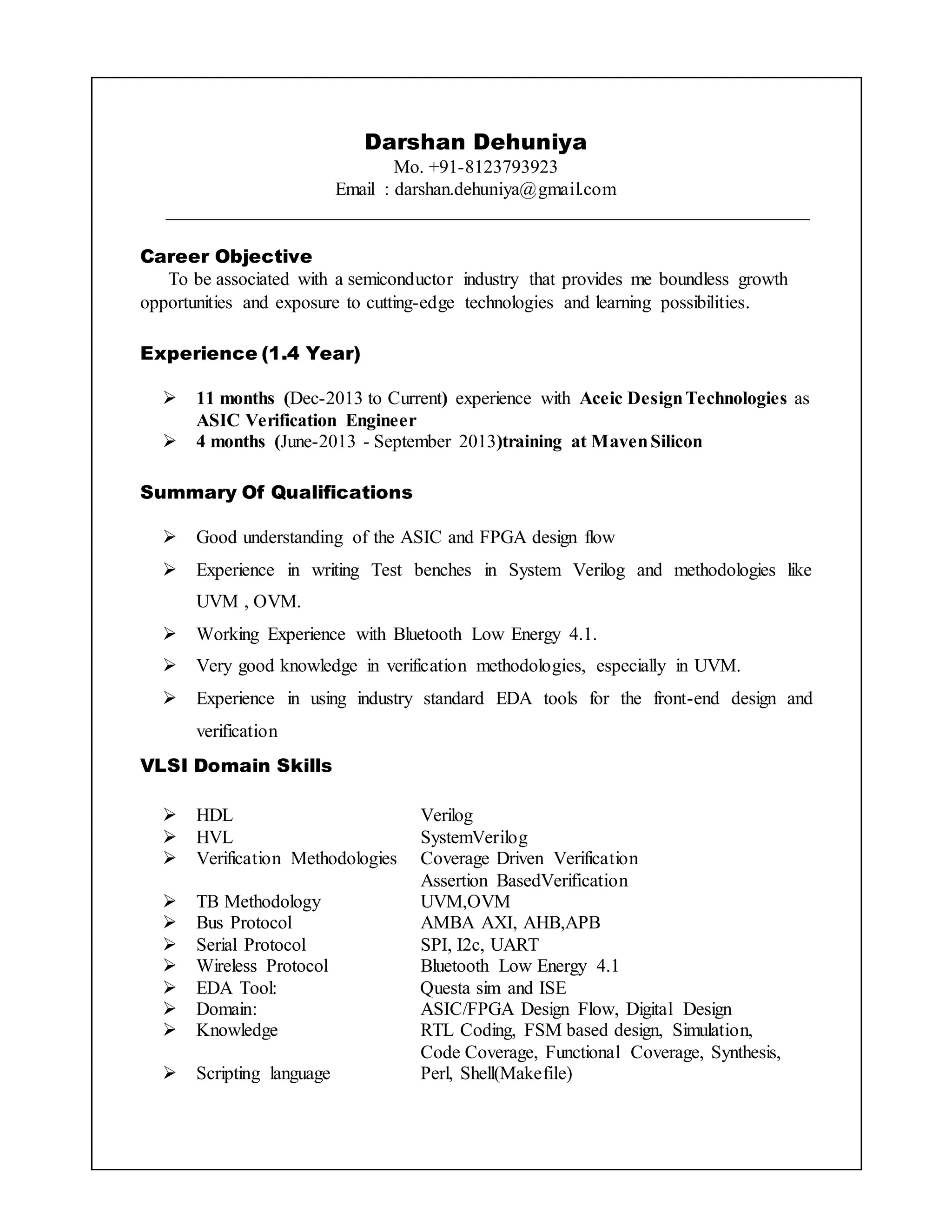
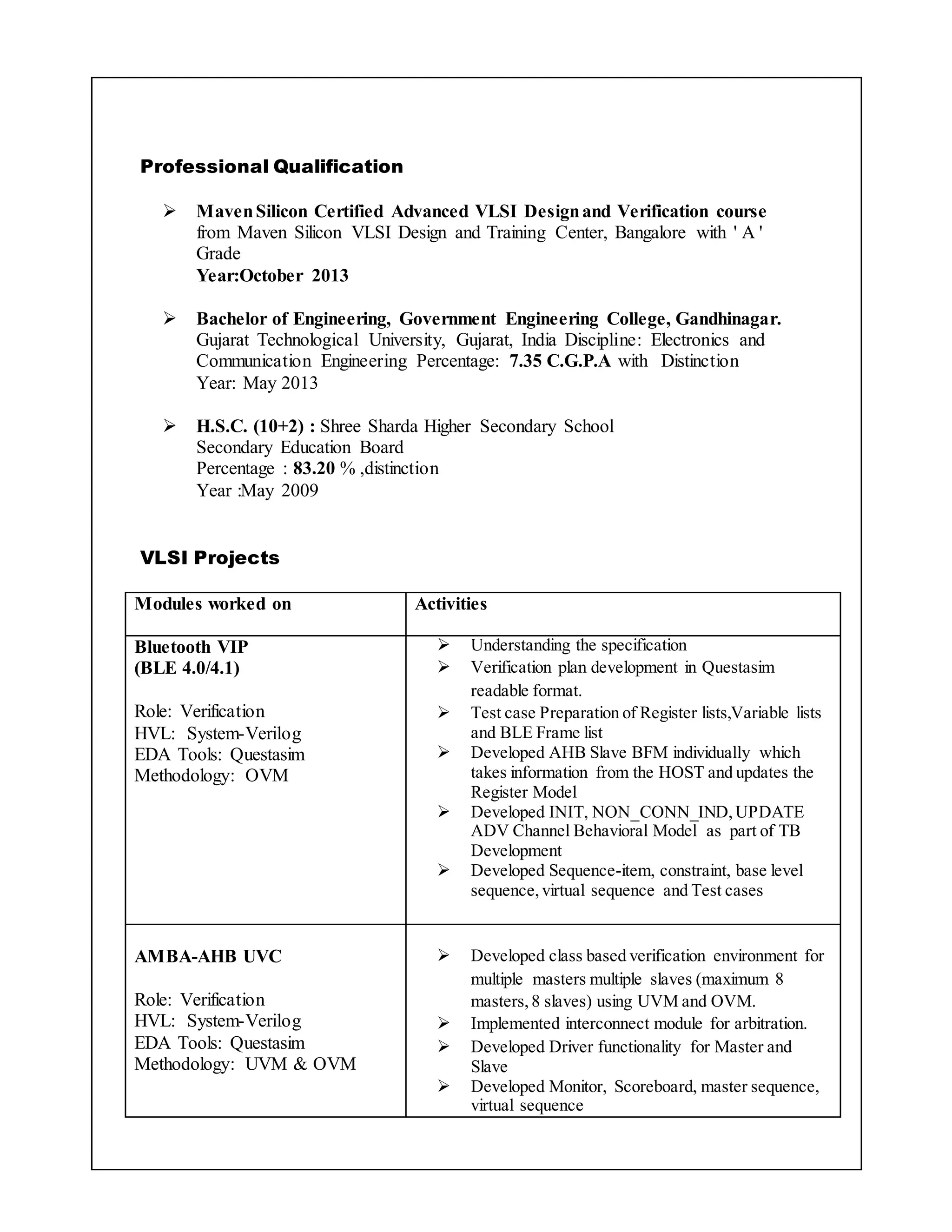

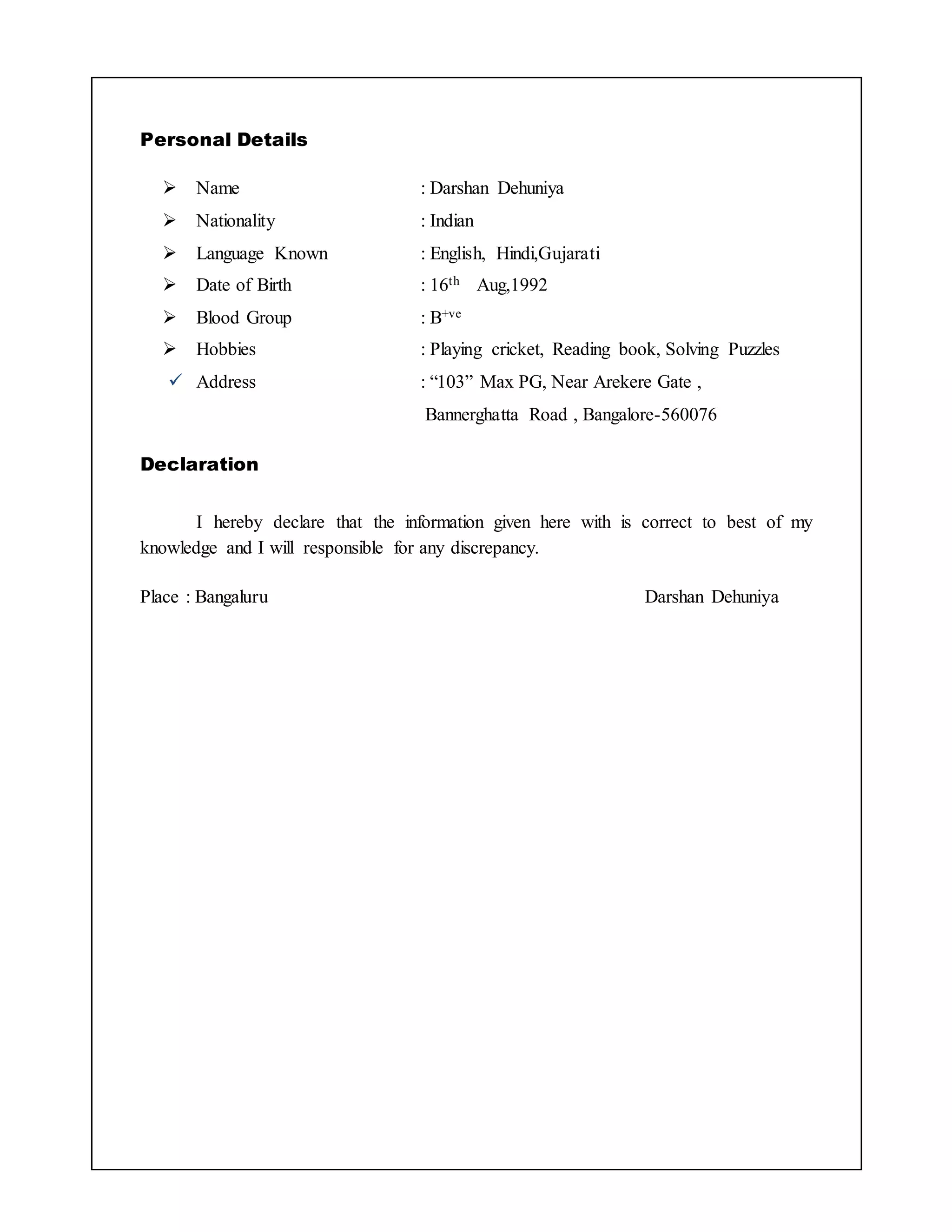

This document contains the resume of Darshan Dehuniya. It summarizes his career objective, qualifications, skills, and experience. He has over 1.4 years of experience as an ASIC Verification Engineer. His skills include SystemVerilog, UVM/OVM methodologies, Bluetooth Low Energy 4.1, AMBA protocols, and FPGA/ASIC design flows. He has a Bachelor's degree in Electronics and Communication Engineering and has worked on projects involving Bluetooth, AMBA, AXI, UART, and SPI verification.