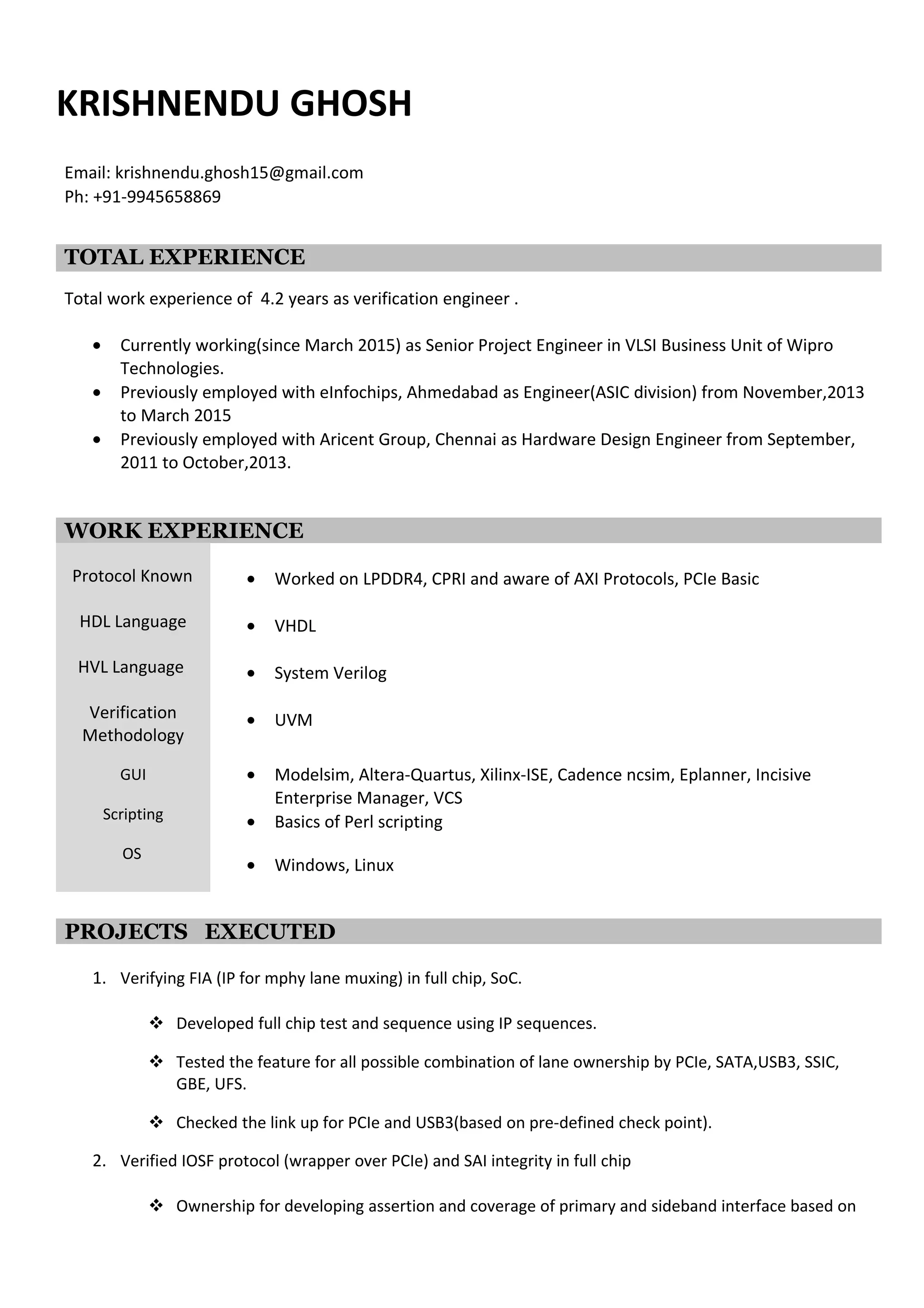
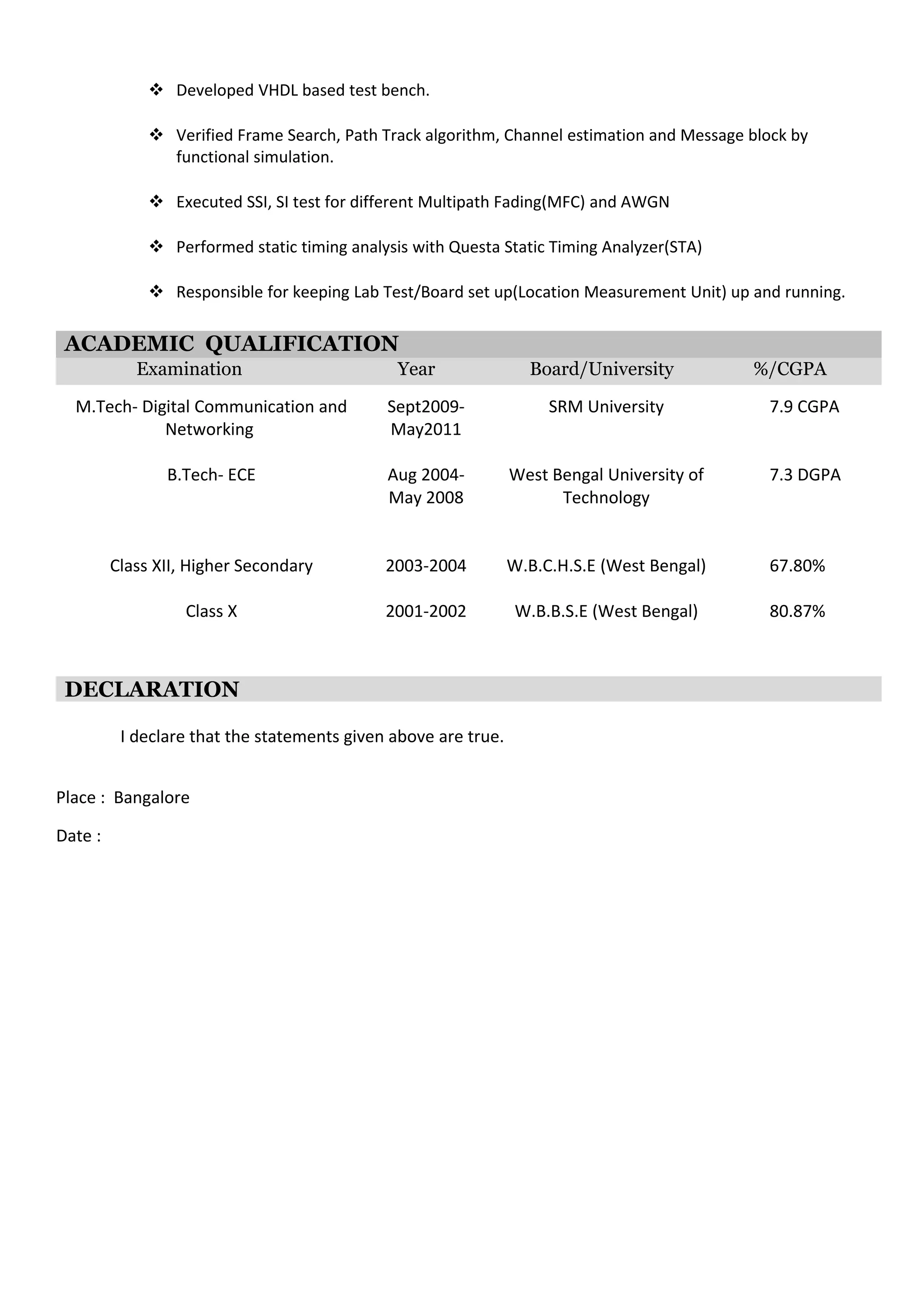
KRISHNENDU GHOSH
Email: krishnendu.ghosh15@gmail.com
Ph: +91-9945658869
TOTAL EXPERIENCE
Total work experience of around 5 years as verification engineer .
• Currently working(since March 2015) as Senior Project Engineer in VLSI Business Unit of Wipro
Technologies.
• Previously employed with eInfochips, Ahmedabad as Engineer(ASIC division) from November,2013
to March 2015
• Previously employed with Aricent Group, Chennai as Hardware Design Engineer from September,
2011 to October,2013.
• 6 month as Project Intern during final year of Masters.
WORK EXPERIENCE
Protocol Known
HDL Language
HVL Language
Verification
Methodology
GUI
Scripting
OS
• Worked on LPDDR4, CPRI and aware of AXI Protocols, PCIe Basic
• VHDL
• System Verilog
• UVM
• Modelsim, Altera-Quartus, Xilinx-ISE, Cadence ncsim, Eplanner, Incisive
Enterprise Manager, VCS
• Basics of Perl scripting
• Windows, Linux
PROJECTS EXECUTED
1. Verifying FIA (IP for mphy lane muxing) in full chip, SoC.
 Developed full chip test and sequence using IP sequences.
 Tested the feature for all possible combination of lane ownership by PCIe, SATA,USB3, SSIC,
GBE, UFS.
 Checked the link up for PCIe and USB3(based on pre-defined check point).
2. Verified IOSF protocol (wrapper over PCIe) and SAI integrity in full chip
 Ownership for developing assertion and coverage of primary and sideband interface based on
the IOSF protocol.
 Guided the team, to understand the basic debug on the assertion failure in their respective
IP.
3. Verifying block level functionality and integrity check for clock/reset, sync/tod and PA bus block in
FPGA(LANAI).
 Had ownership for clock/reset, sync/tod and PA-BUS block.
 Made verification plan for respective blocks.
 Developed iUVC for PA-BUS.
 Implemented assertion, coverage and test scenario as defined in v-plan.
 Developed C side HAL, SV side DPI for HAL. Verified the HAL and used for register read write.
 Executed verification closure with functional and code coverage.
4. Verifying LPDDR4 engine through PA-BUS interface
 Created verification plan for LPDDR4 functionality check.
 Developed lpddr4-converter to map top level write, read, activate, deselect command into
lpddr4 pin level command through pa bus interface.
 Developed u-code interface,lpddr4-coverage interface and integrated into environment .
 Developed the coverage class, module and v-unit for lpddr4 and integrated.
 Developed assertion v-unit module and integrated.
 Created the test scenarios as per the v-plan.
5. Verification of CPRI Interface protocol
 Developed System Verilog based test environment to check CPRI interface.
 Created the BFM to mimic CPRI RTL.
 Developed the verification plan and the verification component.
6. System Verilog verification environment for FIFO controller
 Developed System Verilog based test environment to check FIFO controller.
 Developed the verification plan and the verification component
7. Location Measurement Unit for 3G UMTS system – Demodulator Design
 Integrated the path detection module in top design
 Developed VHDL based test bench.
 Verified Frame Search, Path Track algorithm, Channel estimation and Message block by
functional simulation.
 Executed SSI, SI test for different Multipath Fading(MFC) and AWGN
 Performed static timing analysis with Questa Static Timing Analyzer(STA)
 Responsible for keeping Lab Test/Board set up(Location Measurement Unit) up and running.
ACADEMIC QUALIFICATION
Examination Year Board/University %/CGPA
M.Tech- Digital Communication and
Networking
B.Tech- ECE
Sept2009-
May2011
Aug 2004-
May 2008
SRM University
West Bengal University of
Technology
7.9 CGPA
7.3 DGPA
Class XII, Higher Secondary 2003-2004 W.B.C.H.S.E (West Bengal) 67.80%
Class X 2001-2002 W.B.B.S.E (West Bengal) 80.87%
DECLARATION
I declare that the statements given above are true.
Place : Bangalore
Date :

Resume_Krishnendu_Ghosh

  • 1.
    KRISHNENDU GHOSH Email: krishnendu.ghosh15@gmail.com Ph:+91-9945658869 TOTAL EXPERIENCE Total work experience of around 5 years as verification engineer . • Currently working(since March 2015) as Senior Project Engineer in VLSI Business Unit of Wipro Technologies. • Previously employed with eInfochips, Ahmedabad as Engineer(ASIC division) from November,2013 to March 2015 • Previously employed with Aricent Group, Chennai as Hardware Design Engineer from September, 2011 to October,2013. • 6 month as Project Intern during final year of Masters. WORK EXPERIENCE Protocol Known HDL Language HVL Language Verification Methodology GUI Scripting OS • Worked on LPDDR4, CPRI and aware of AXI Protocols, PCIe Basic • VHDL • System Verilog • UVM • Modelsim, Altera-Quartus, Xilinx-ISE, Cadence ncsim, Eplanner, Incisive Enterprise Manager, VCS • Basics of Perl scripting • Windows, Linux PROJECTS EXECUTED 1. Verifying FIA (IP for mphy lane muxing) in full chip, SoC.  Developed full chip test and sequence using IP sequences.  Tested the feature for all possible combination of lane ownership by PCIe, SATA,USB3, SSIC, GBE, UFS.  Checked the link up for PCIe and USB3(based on pre-defined check point). 2. Verified IOSF protocol (wrapper over PCIe) and SAI integrity in full chip
  • 2.
     Ownership fordeveloping assertion and coverage of primary and sideband interface based on the IOSF protocol.  Guided the team, to understand the basic debug on the assertion failure in their respective IP. 3. Verifying block level functionality and integrity check for clock/reset, sync/tod and PA bus block in FPGA(LANAI).  Had ownership for clock/reset, sync/tod and PA-BUS block.  Made verification plan for respective blocks.  Developed iUVC for PA-BUS.  Implemented assertion, coverage and test scenario as defined in v-plan.  Developed C side HAL, SV side DPI for HAL. Verified the HAL and used for register read write.  Executed verification closure with functional and code coverage. 4. Verifying LPDDR4 engine through PA-BUS interface  Created verification plan for LPDDR4 functionality check.  Developed lpddr4-converter to map top level write, read, activate, deselect command into lpddr4 pin level command through pa bus interface.  Developed u-code interface,lpddr4-coverage interface and integrated into environment .  Developed the coverage class, module and v-unit for lpddr4 and integrated.  Developed assertion v-unit module and integrated.  Created the test scenarios as per the v-plan. 5. Verification of CPRI Interface protocol  Developed System Verilog based test environment to check CPRI interface.  Created the BFM to mimic CPRI RTL.  Developed the verification plan and the verification component. 6. System Verilog verification environment for FIFO controller  Developed System Verilog based test environment to check FIFO controller.  Developed the verification plan and the verification component 7. Location Measurement Unit for 3G UMTS system – Demodulator Design  Integrated the path detection module in top design
  • 3.
     Developed VHDLbased test bench.  Verified Frame Search, Path Track algorithm, Channel estimation and Message block by functional simulation.  Executed SSI, SI test for different Multipath Fading(MFC) and AWGN  Performed static timing analysis with Questa Static Timing Analyzer(STA)  Responsible for keeping Lab Test/Board set up(Location Measurement Unit) up and running. ACADEMIC QUALIFICATION Examination Year Board/University %/CGPA M.Tech- Digital Communication and Networking B.Tech- ECE Sept2009- May2011 Aug 2004- May 2008 SRM University West Bengal University of Technology 7.9 CGPA 7.3 DGPA Class XII, Higher Secondary 2003-2004 W.B.C.H.S.E (West Bengal) 67.80% Class X 2001-2002 W.B.B.S.E (West Bengal) 80.87% DECLARATION I declare that the statements given above are true. Place : Bangalore Date :