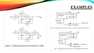
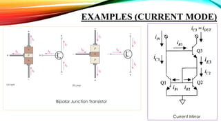
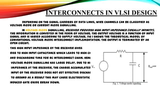
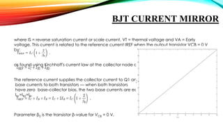
This document discusses current mode and voltage mode circuits. It begins by defining voltage mode and current mode circuits, noting that the definitions are not entirely precise as every circuit has both voltages and currents. It then provides examples of current mode circuits including the bipolar junction transistor and current mirror. It discusses how current mode and voltage mode signaling works for interconnects in integrated circuits. It notes several advantages of current mode circuits including lower power consumption and higher speed. It also discusses differences between the two modes and reasons for switching to current mode circuits such as easier compensation and better operation in continuous and discontinuous conduction modes. Potential disadvantages of current mode are also outlined like current sensing challenges and subharmonic oscillations.
Field Effect Transistor, JFET, Metal Oxide Semiconductor Field Effect Transistor, Depletion MOSFET, Enhancement MoSFET, Construction, Basic operation, Regions of Operation, Drain Characteristics, Transfer Characteristics, Biasing, Non-Ideal Characteristics of E-MOSFET, DC Analysis, AC equivalent circuit and Parameters, E-MOSFET as an Amplifier, AC analysis, MOSFET as a Switch, MOSFET as a diode, MOSFET as a resistor, High frequency equivalent circuit, Miller Capacitance, Frequency Response, NMOS and CMOS inverter
The MOSFET is an important element in embedded system design which is used to control the loads as per the requirement. The MOSFET is a high voltage controlling device provides some key features for circuit designers in terms of their overall performance.
Mosfet
MOSFETs have characteristics similar to JFETs and additional characteristics that make them very useful.
There are 2 types:
• Depletion-Type MOSFET
• Enhancement-Type MOSFET
The presentation covers Bipolar Junction Transistor: Construction, Operation, Transistor configurations and input / output characteristics; Common Base, Common Emitter, and Common Collector
The metal–oxide–semiconductor field-effect transistor (MOSFET, MOS-FET, or MOS FET) is a type of field-effect transistor (FET). It has an insulated gate, whose voltage determines the conductivity of the device. This ability to change conductivity with the amount of applied voltage can be used for amplifying or switching electronic signals. Although FET is sometimes used when referring to MOSFET devices, other types of field-effect transistors also exist.
This presentation discusses the basics of Pass Transistor Logic, its advantages, limitation and finally implementation of Boolean functions/Combinational Logic circuits using Pass Transistor Logic.
The three terminals of the FET are known as Gate, Drain, and Source.
It is a voltage controlled device, where the input voltage controls by the output current.
In FET current used to flow between the drain and the source terminal. And this current can be controlled by applying the voltage between the gate and the source terminal.
So this applied voltage generate the electric field within the device and by controlling these electric field we can control the flow of current through the device.
Field-effect transistor amplifiers provide an excellent voltage gain with the added feature of high input impedance. They are also low-power-consumption configurations with good frequency range and minimal size and weight.
JFETs, depletion MOSFETs, and MESFETs can be used to design amplifiers having similar voltage gains.
The depletion MOSFET (MESFET) circuit, however, has a much higher input impedance than a similar JFET configuration.
Review of Step down Converter with Efficient ZVS OperationIJRST Journal
This paper presents the review of step down converter with efficient ZVS operation. The designed buck converter uses ZCS technique and the function is realized so that the power form is converted from 12V DC 5V DC (1A). A detailed analysis of zero current switching buck converters is performed and a mathematical analysis of the mode of operation is also presented. In order to reduce the switching losses in associated with conventional converters; resonant inductor and resonant capacitor (LC resonant circuit) is applied which helps to turn on-off the switch at zero current. The dc-dc buck converter receives the energy from the input source, when the switch is turned-on. The buck–buck converters have characteristics that warrant a more detailed study. The buck converters under discontinuous conduction mode /continuous conduction mode boundary.
Speed Control Of Separately Excited Dc Motor Using A High Efficiency Flyback ...IJERA Editor
This paper deals with Speed control of separately excited DC motor using flyback converter with a new non complementary active clamp control method to achieve soft switching and high efficiency for heavy motor load and light load conditions. This is quite attractive for low power application with universal ac inputs, such as external adaptors. With the proposed control technique, the energy in the leakage inductance can be fully recycled. The soft switching can be achieved for the main switch and the absorbed leakage energy is transferred to the output and input side. In the Proposed model the resistive and DC motor is connected to flyback converter and it is simulated with different nominal voltages and rated speed is controlled at different levels for the N-type active clamp flyback converter and P-type active clamp flyback converter respectively. N-type active clamp flyback converter is suitable for high speed variation applications and P-type active clamp flyback converter is suitable for low speed variation applications.
Signal conditioning is useful in making of the circuits related to small signals and setting the signals ranges. Sensors are having different outputs and we can set the desired ranges of the voltages as per the necessity.
Fuzzy Logic Controller Based High Frequency Link AC-AC Converter For Voltage ...IJTET Journal
Abstract—In this paper, an advanced high frequency link AC-AC Push-pull cycloconverter for the voltage compensation is proposed in order to maintain the power quality in electric grid. The proposed methodology can be achieve arbitrary output voltage without using large energy storage elements. So that the system is more steadfast and less costly compared with the conventional inverter topology. Additionally, the proposed converter does not contain any line frequency transformer, which reduces the cost further. The control scheme for the push pull cycloconverter employs the fuzzy logic controller based sinusoidal pulse width modulation (SPWM) to accomplish better performance on voltage compensation, like unbalanced voltage harmonics elimination. The simulation results are given to show the effectiveness of the proposed high frequency link AC-AC converter and fuzzy logic controller based SPWM technology
Introduction to AI for Nonprofits with Tapp NetworkTechSoup
Dive into the world of AI! Experts Jon Hill and Tareq Monaur will guide you through AI's role in enhancing nonprofit websites and basic marketing strategies, making it easy to understand and apply.
Model Attribute Check Company Auto PropertyCeline George
In Odoo, the multi-company feature allows you to manage multiple companies within a single Odoo database instance. Each company can have its own configurations while still sharing common resources such as products, customers, and suppliers.
Welcome to TechSoup New Member Orientation and Q&A (May 2024).pdfTechSoup
In this webinar you will learn how your organization can access TechSoup's wide variety of product discount and donation programs. From hardware to software, we'll give you a tour of the tools available to help your nonprofit with productivity, collaboration, financial management, donor tracking, security, and more.
How to Make a Field invisible in Odoo 17Celine George
It is possible to hide or invisible some fields in odoo. Commonly using “invisible” attribute in the field definition to invisible the fields. This slide will show how to make a field invisible in odoo 17.
Embracing GenAI - A Strategic ImperativePeter Windle
Artificial Intelligence (AI) technologies such as Generative AI, Image Generators and Large Language Models have had a dramatic impact on teaching, learning and assessment over the past 18 months. The most immediate threat AI posed was to Academic Integrity with Higher Education Institutes (HEIs) focusing their efforts on combating the use of GenAI in assessment. Guidelines were developed for staff and students, policies put in place too. Innovative educators have forged paths in the use of Generative AI for teaching, learning and assessments leading to pockets of transformation springing up across HEIs, often with little or no top-down guidance, support or direction.
This Gasta posits a strategic approach to integrating AI into HEIs to prepare staff, students and the curriculum for an evolving world and workplace. We will highlight the advantages of working with these technologies beyond the realm of teaching, learning and assessment by considering prompt engineering skills, industry impact, curriculum changes, and the need for staff upskilling. In contrast, not engaging strategically with Generative AI poses risks, including falling behind peers, missed opportunities and failing to ensure our graduates remain employable. The rapid evolution of AI technologies necessitates a proactive and strategic approach if we are to remain relevant.
The Roman Empire A Historical Colossus.pdfkaushalkr1407
The Roman Empire, a vast and enduring power, stands as one of history's most remarkable civilizations, leaving an indelible imprint on the world. It emerged from the Roman Republic, transitioning into an imperial powerhouse under the leadership of Augustus Caesar in 27 BCE. This transformation marked the beginning of an era defined by unprecedented territorial expansion, architectural marvels, and profound cultural influence.
The empire's roots lie in the city of Rome, founded, according to legend, by Romulus in 753 BCE. Over centuries, Rome evolved from a small settlement to a formidable republic, characterized by a complex political system with elected officials and checks on power. However, internal strife, class conflicts, and military ambitions paved the way for the end of the Republic. Julius Caesar’s dictatorship and subsequent assassination in 44 BCE created a power vacuum, leading to a civil war. Octavian, later Augustus, emerged victorious, heralding the Roman Empire’s birth.
Under Augustus, the empire experienced the Pax Romana, a 200-year period of relative peace and stability. Augustus reformed the military, established efficient administrative systems, and initiated grand construction projects. The empire's borders expanded, encompassing territories from Britain to Egypt and from Spain to the Euphrates. Roman legions, renowned for their discipline and engineering prowess, secured and maintained these vast territories, building roads, fortifications, and cities that facilitated control and integration.
The Roman Empire’s society was hierarchical, with a rigid class system. At the top were the patricians, wealthy elites who held significant political power. Below them were the plebeians, free citizens with limited political influence, and the vast numbers of slaves who formed the backbone of the economy. The family unit was central, governed by the paterfamilias, the male head who held absolute authority.
Culturally, the Romans were eclectic, absorbing and adapting elements from the civilizations they encountered, particularly the Greeks. Roman art, literature, and philosophy reflected this synthesis, creating a rich cultural tapestry. Latin, the Roman language, became the lingua franca of the Western world, influencing numerous modern languages.
Roman architecture and engineering achievements were monumental. They perfected the arch, vault, and dome, constructing enduring structures like the Colosseum, Pantheon, and aqueducts. These engineering marvels not only showcased Roman ingenuity but also served practical purposes, from public entertainment to water supply.
June 3, 2024 Anti-Semitism Letter Sent to MIT President Kornbluth and MIT Cor...Levi Shapiro
Letter from the Congress of the United States regarding Anti-Semitism sent June 3rd to MIT President Sally Kornbluth, MIT Corp Chair, Mark Gorenberg
Dear Dr. Kornbluth and Mr. Gorenberg,
The US House of Representatives is deeply concerned by ongoing and pervasive acts of antisemitic
harassment and intimidation at the Massachusetts Institute of Technology (MIT). Failing to act decisively to ensure a safe learning environment for all students would be a grave dereliction of your responsibilities as President of MIT and Chair of the MIT Corporation.
This Congress will not stand idly by and allow an environment hostile to Jewish students to persist. The House believes that your institution is in violation of Title VI of the Civil Rights Act, and the inability or
unwillingness to rectify this violation through action requires accountability.
Postsecondary education is a unique opportunity for students to learn and have their ideas and beliefs challenged. However, universities receiving hundreds of millions of federal funds annually have denied
students that opportunity and have been hijacked to become venues for the promotion of terrorism, antisemitic harassment and intimidation, unlawful encampments, and in some cases, assaults and riots.
The House of Representatives will not countenance the use of federal funds to indoctrinate students into hateful, antisemitic, anti-American supporters of terrorism. Investigations into campus antisemitism by the Committee on Education and the Workforce and the Committee on Ways and Means have been expanded into a Congress-wide probe across all relevant jurisdictions to address this national crisis. The undersigned Committees will conduct oversight into the use of federal funds at MIT and its learning environment under authorities granted to each Committee.
• The Committee on Education and the Workforce has been investigating your institution since December 7, 2023. The Committee has broad jurisdiction over postsecondary education, including its compliance with Title VI of the Civil Rights Act, campus safety concerns over disruptions to the learning environment, and the awarding of federal student aid under the Higher Education Act.
• The Committee on Oversight and Accountability is investigating the sources of funding and other support flowing to groups espousing pro-Hamas propaganda and engaged in antisemitic harassment and intimidation of students. The Committee on Oversight and Accountability is the principal oversight committee of the US House of Representatives and has broad authority to investigate “any matter” at “any time” under House Rule X.
• The Committee on Ways and Means has been investigating several universities since November 15, 2023, when the Committee held a hearing entitled From Ivory Towers to Dark Corners: Investigating the Nexus Between Antisemitism, Tax-Exempt Universities, and Terror Financing. The Committee followed the hearing with letters to those institutions on January 10, 202
2. INTRODUCTION
Voltage-Mode:Information is represented by voltage at the nodes of the circuit.
Current-Mode:Information is represented by current flowing in the branches of the circuit.
However, none of the definitions used in the literature are precise. For
example, some authors write that signals are represented by currents in currentmode circuits and by voltages in voltage-mode circuits. This is not a precise
definition, because every circuit node has an associated voltage and every branch an
associated current. Therefore, current-mode and voltage-mode do not actually
divide circuits into two categories, they are just alternate ways of looking at a
circuit.
5. INTERCONNECTS IN VLSI DESIGN
Depending on the signal carriers of data links, wire channels can be classified as
voltage mode or current mode signalling.
In voltage mode signalling, receiver provides high input impedance (ideally infinity).
The information is conveyed in the form of voltage. The output voltage is a function of input
signal and is varied according to supply voltage. Fig 1 shows the theoretical model of
conventional voltage mode interconnect implementation. The output is terminated by an
open circuit.
This high input impedance of the receiver gives
rise to high input capacitance which leads to high charging
and discharging time for RC interconnect chain. Hence
voltage mode signalling has large delay. Due to high input
impedance at the receiver, the charge accumulated at the
input of the receiver does not get effective discharge path
to ground as a result this may cause electrostatic
induced gate oxide break down.
7. DIFFERENCES
In integrated circuits, current-mode offers some advantages over voltage-mode :
o Performances improvement
low power consumption at high frequency
less affected by voltage fluctuations
low cross-talk & switching noise
high speed
o Structural advantages
controlled gain without feedback components
current summing without components
schematic simplicity
o Specific features
well suited for low voltage, low power applications
pseudo conductance networks
current switching technique
8. WHY WE SWITCH TO THE CURRENT MODE
CIRCUITS?
#1: Easy Compensation
• With voltage-mode, the sharp phase drop after the filter resonant frequency requires a
type three compensator to stabilize the system.
• Current-mode control looks like a single-pole system at low frequencies, since the
inductor has been controlled by the current loop.
• This improves the phase margin, and makes the converter much easier to control.
• A type two compensator is adequate, which greatly simplifies the design process.
9. WHY WE SWITCH TO THE CURRENT MODE
CIRCUITS?
#2: RHP Zero Converters
• Contrary to some papers on the topic, current-mode control does NOT eliminate the right-half
plane (RHP) zero of boost, flyback, and other converters.
• It does make compensation of such converters easier, though.
• With voltage-mode control, crossover has to be well above the resonant frequency, or the
filter will ring.
• In a converter where the crossover frequency is restricted by the presence of an RHP zero, this
could be impossible.
• It's not a problem with current-mode control to have a control loop crossover at or below the
filter resonant frequency.
10. WHY WE SWITCH TO THE CURRENT MODE
CIRCUITS?
#3: CCM and DCM Operation
• When moving from continuous-conduction
mode (CCM) to discontinuous-conduction
mode (DCM), the characteristics with voltagemode control are drastically different as shown
in Fig 4.
• It is not possible to design a compensator with
voltage-mode that can provide good
performance in both regions. With currentmode, crossing the boundary between the two
types of operation is not a problem. The
characteristics are almost constant in the region
of crossover, as shown in Figure 5.
• Having optimal response in both modes is a
major advantage, allowing the power stage to
operate much more efficiently. Keeping a
converter in DCM for all changes of load, line,
temperature, transients, and other parameter
variations can lead to severe component
stresses.
11. WHY WE SWITCH TO THE CURRENT MODE
CIRCUITS?
#4: Line Rejection
• Closing the current loop gives a lot of attenuation of input noise. For the buck, it
can even be nulled under some special conditions, with the proper compensating
saw-tooth ramp.
• Even with only a moderate gain in the voltage feedback loop, the attenuation of
input ripple is usually adequate with current-mode control.
• With voltage-mode control, far more gain is needed in the main feedback loop to
achieve the same performance.
12. DISADVANTAGES OF CURRENT MODE
#1: Current Sensing
• Either the switch current or inductor current must be sensed accurately.
• This requires additional circuitry, and some power loss.
• In most isolated power supplies, the switch current is sensed either with a resistor or
current transformer.
• The current sensing must be very wideband to accurately reconstruct the current signal.
• A current transformer needs a bandwidth several orders of magnitude above the
switching frequency to work dependably.
13. DISADVANTAGES OF CURRENT MODE
#2: Sub harmonic Oscillations Instability
• Current-mode control can be unstable when the duty cycle of the converter
approaches 50%.
• This does not occur abruptly at 50%, as some data books claim, but can manifest
the problem even at lower duty cycles.
• A compensating ramp is needed to fix the problem, and this too can introduce
complications.
14. DISADVANTAGES OF CURRENT MODE
#3: Signal-to-Noise Ratio
• The biggest problem in almost every currentmode supply is noise on the current sense signal.
• In many power supplies there is simply not enough
signal to control the converter smoothly over
the full range of operation.
• Even with the ideal current waveform of Figure 6a,
the signal available for control is small.
• The peak of the current signal is limited by the
PWM controller, usually to less than 1 V.
• Much of the available signal range can be taken by
the DC value of the switch current. When the real
current waveform of Figure with spikes and
ringing is considered, the problem becomes even
worse.
15. BJT CURRENT MIRROR
If a voltage is applied to the BJT base-emitter junction as an input quantity and the collector
current is taken as an output quantity, the transistor will act as an exponential voltage-to-current
converter. By applying a negative feedback (simply joining the base and collector) the transistor can be
"reversed" and it will begin acting as the opposite logarithmic current-to-voltage converter; now it
will adjust the "output" base-emitter voltage so as to pass the applied "input" collector current.
The simplest bipolar current mirror implements this idea. It
consists of two cascaded transistor stages acting accordingly as a
reversed and direct voltage-to-current converters. Transistor Q1
is connected to ground. Its collector-base voltage is zero as
shown. Consequently, the voltage drop across Q1 is VBE, that is, this
voltage is set by the diode law and Q1 is said to be diode
connected. It is important to have Q1 in the circuit instead of a
simple diode, because Q1 sets VBE for transistor Q2. If Q1 and Q2 are
matched, that is, have substantially the same device properties,
and if the mirror output voltage is chosen so the collector-base
voltage of Q2 is also zero, then the VBE-value set by Q1 results in
an emitter current in the matched Q2 that is the same as the
emitter current in Q1. Because Q1 and Q2 are matched, their β0values also agree, making the mirror output current the same as
the collector current of Q1. The current delivered by the mirror
for arbitrary collector-base reverse bias VCB of the output
16. BJT CURRENT MIRROR
where IS = reverse saturation current or scale current, VT = thermal voltage and VA = Early
voltage. This current is related to the reference current IREF when the output transistor VCB = 0 V
by:
as found using Kirchhoff's current law at the collector node of Q1:
The reference current supplies the collector current to Q1 and the
base currents to both transistors — when both transistors
have zero base-collector bias, the two base currents are equal,
IB1=IB2=IB.
Parameter β0 is the transistor β-value for VCB = 0 V.
17. IIIrd Semester Self Study Project
by:-
Gajera Kevin, EC/066
Gautam Rathee, EC/069
Shaleen Rathode, EC/161
Nag Mani, EC/102